High isolation antenna array using SIW and realized with a graphene layer for sub terahertz wireless applications - Nature
←
→
Page content transcription
If your browser does not render page correctly, please read the page content below
www.nature.com/scientificreports
OPEN High‑isolation antenna array using
SIW and realized with a graphene
layer for sub‑terahertz wireless
applications
Mohammad Alibakhshikenari1*, Bal S. Virdee2, Shahram Salekzamankhani2, Sonia Aïssa3,
Chan H. See4, Navneet Soin5, Sam J. Fishlock5, Ayman A. Althuwayb6, Raed Abd‑Alhameed7,
Isabelle Huynen8, James A. McLaughlin5, Francisco Falcone9,10 & Ernesto Limiti1
This paper presents the results of a study on developing an effective technique to increase the
performance characteristics of antenna arrays for sub-THz integrated circuit applications. This is
essential to compensate the limited power available from sub-THz sources. Although conventional
array structures can provide a solution to enhance the radiation-gain performance however in the
case of small-sized array structures the radiation properties can be adversely affected by mutual
coupling that exists between the radiating elements. It is demonstrated here the effectiveness of
using SIW technology to suppress surface wave propagations and near field mutual coupling effects.
Prototype of 2 × 3 antenna arrays were designed and constructed on a polyimide dielectric substrate
with thickness of 125 μm for operation across 0.19–0.20 THz. The dimensions of the array were
20 × 13.5 × 0.125 mm3. Metallization of the antenna was coated with 500 nm layer of Graphene. With
the proposed technique the isolation between the radiating elements was improved on average by
22.5 dB compared to a reference array antenna with no SIW isolation. The performance of the array
was enhanced by transforming the patch to exhibit metamaterial characteristics. This was achieved
by embedding the patch antennas in the array with sub-wavelength slots. Compared to the reference
array the metamaterial inspired structure exhibits improvement in isolation, radiation gain and
efficiency on average by 28 dB, 6.3 dBi, and 34%, respectively. These results show the viability of
proposed approach in developing antenna arrays for application in sub-THz integrated circuits.
Wireless communication bands are increasingly becoming highly crowded and the ever-increasing demand
for more bandwidth has provoked the exploitation of the yet unexplored electromagnetic spectrum in the sub-
terahertz (THz) region1. Higher bandwidth afforded by the sub-terahertz band can achieve extremely high
data-rates in the order of 0.1 THz/s for future wireless s ystems2. However, sub-terahertz radiation is absorbed by
most materials, including the molecules in the atmosphere such as water vapor. For such systems, line-of-sight
propagation is needed and even for such conditions, the range is rather limited due to the inherently high path-
loss. Since path-loss is relatively high and the current sub-THz receivers are not sensitive, hence much effort
needs to be devoted on maximizing both the radiation-gain and efficiency of sub-terahertz antennas.
Owing to the lack of sub-terahertz sources and detectors, this area of the electromagnetic spectrum has not
been fully explored for wireless communication a pplications3. The up and down-converters as well as low-gain
1
Electronic Engineering Department, University of Rome “Tor Vergata”, Via del Politecnico 1, 00133 Rome,
Italy. 2Center for Communications Technology & Mathematics, School of Computing and Digital Media,
London Metropolitan University, London N7 8DB, UK. 3Institut National de La Recherche Scientifique (INRS),
University of Quebec, Montréal, QC H5A 1K6, Canada. 4School of Engineering and the Built Environment,
Edinburgh Napier University, Edinburgh, UK. 5School of Engineering, Ulster University, Newtownabbey, Belfast,
Northern Ireland BT37 0QB, UK. 6Electrical Engineering Department, Jouf University, Sakaka 72388, Saudi
Arabia. 7Faculty of Engineering and Informatics, University of Bradford, Bradford, UK. 8Institute of Information
and Communication Technologies, Electronics and Applied Mathematics, Université Catholique de Louvain,
Ottignies‑Louvain‑la‑Neuve, Belgium. 9Electric, Electronic and Communication Engineering Department,
Public University of Navarre, 31006 Pamplona, Spain. 10Institute of Smart Cities, Public University of Navarre,
31006 Pamplona, Spain. *email: alibakhshikenari@ing.uniroma2.it
Scientific Reports | (2021) 11:10218 | https://doi.org/10.1038/s41598-021-87712-y 1
Vol.:(0123456789)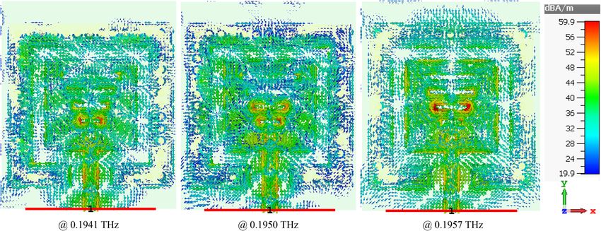
www.nature.com/scientificreports/
Figure 1. Antenna structure: (a) reference antenna with no SIW technology, (b) and (c) the proposed antenna
with SIW technology.
Figure 2. Scanning electron microscope (SEM) image of polyimide substrate (65º tilt angle) to highlight how
the vias are fabricated by increasing the scribing laser power to ‘punch’ through the substrate and create an
electrically conducting through-connection.
amplifiers constituting the RF front-end of sub-terahertz communication system have restricted output power
and bandwidth. Existing technology relies on mixing optical sources essentially lasers to generate low to moder-
ate power-levels at sub-THz band. Receivers at such frequencies rely on direct detection using Schottky-diodes,
which is not band selective and has a low dynamic range and s ensitivity4.
At sub-THz frequencies metals exhibit a lower conductivity than at DC. This phenomenon enhances field
infiltration within the metal at sub-THz and adversely affect the radiation efficiency of metallic antennas5. In
addition to the low conductivity of metal at these frequencies, the effect of small geometric parameters of metallic
antennas, specifically the width or radius of metallic traces which are smaller than 0.1 micron, must be consid-
ered. This is because numerical analysis reveals that small scale antennas of sub-100 nano-meters compared to
their millimeter-sized counterparts results in significantly low radiation efficiency at sub-THz frequency due to
the high surface resistance of metallic t races6. Moreover, because of the method employed for conductor deposi-
tion in the fabrication of ultra-thin metallic traces of sub-nano-meter thickness, the magnitude of the metal’s
conductivity becomes considerably lower than that of the bulk material. The low conductivity is attributed to
the following factors: grain boundary scattering, surface scattering, and surface r oughness7, 8. These factors can
considerably reduce the theoretically predicted radiation efficiency of antennas at sub-terahertz frequencies.
Recently various sub-THz antenna arrays have been investigated for THz spectroscopy based on s lots9,
printed dipoles10 or patch antennas11 however the radiation characteristics of these antennas are limited for
practical applications. Hence there is demand for antennas at these frequencies with improved radiation gain
and efficiency characteristics. Although high performance wideband horn antennas are now available12, they
are bulky in structure even at very high frequencies. Instead, low profile planar antennas are desirable for ease
of integration with RF-circuits to realize compact t ransceivers13, 14.
Scientific Reports | (2021) 11:10218 | https://doi.org/10.1038/s41598-021-87712-y 2
Vol:.(1234567890)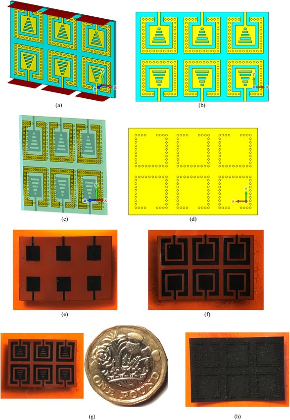
www.nature.com/scientificreports/
Parameter Dimension (mm)
Patch length 3
Patch width 3
Feedline length 2
Feedline width 0.4
SIW isolator width 0.75
Gap between patch and isolator 0.5
Gap between feedline and isolator 0.5
Diameter of vias 0.25
Gap between vias 0.20
Thickness of graphene layer 0.0005
Substrate thickness 0.125
Table 1. Dimensions of the antenna.
Figure 3. Simulated reflection-coefficient response of the reference and SIW-loaded patch antennas.
In this study the isolation, radiation-gain and efficiency of sub-terahertz array structure is improved by
employing a combination of substrate integrated waveguide (SIW) and metamaterial (MTM) inspired tech-
nologies. The prototype antenna arrays were designed and analysed using numerical simulation tools, and the
optimized designs fabricated and measured. The array structures were coated with a thin layer of Graphene as
it supports the propagation of surface plasmon polaritons enabling it to operate in the sub-terahertz frequency
band15, 16. In17 it has been shown that plasmons in graphene layer strongly confine electromagnetic energy, and
in18 it has been shown that the application of a voltage to the graphene layer affects the phase characteristics of
the antenna. These results show Graphene material opens exciting prospects for antenna development in the
terahertz frequency band.
Sub‑terahertz antenna based on SIW Technology
Geometries of the standard reference patch and the proposed SIW-loaded patch antenna are shown in Fig. 1. The
patch antenna was constructed on a polyimide dielectric substrate (Kaneka, Apical NP, USA) with thickness of
125 μm, dielectric constant (εr ) of 3.5, and loss-tangent (tangδ) of 0.0027. To produce the graphene patch, a CO2
laser (Universal Laser 230 VLS) was used to scribe the front and rear polyimide surfaces and thereby convert
this into a graphene film, using the same experimental conditions as discussed in19. To produce the vias, the
laser power was increased from 8.1 W (as used for the standard patch on the front face) to 15 W, and the laser
scribe was repeated twice in these areas, in order to ‘punch’ through the polyimide surface. A cross section of
the via taken using an SEM (Hitachi SU5000 field emission scanning electron microscope) can be observed in
Fig. 2. The proposed antenna includes SIW isolator which is framed around the square patch. Dimensions of the
antenna are given in Table 1. Reflection-coefficient response for both antennas over 0.194–0.196 THz is shown
in Fig. 3. The results reveal SIW isolation improves the impedance match of the antenna, which is pronounced
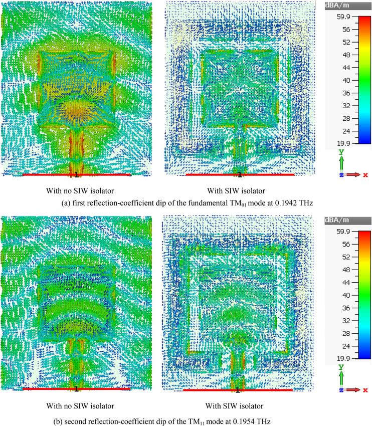
at the resonance frequencies of 0.1942 THz and 0.1954 THz. Surface current density distribution over the two
antennas at their dominant resonant modes in Fig. 4 show the effectiveness of the SIW isolator in suppressing
the propagating surface waves over the structure. Suppression of surface waves is desirable in antenna arrays
to mitigate mutual coupling between adjacent radiating elements and thereby improve the antenna’s radiation
characteristics. Radiation gain and efficiency plots of both antennas at the resonant frequencies in Fig. 5 show
the SIW isolator significantly enhances the radiation-gain and efficiency properties over the reference antenna,
due to reduction in substrate loss.
Scientific Reports | (2021) 11:10218 | https://doi.org/10.1038/s41598-021-87712-y 3
Vol.:(0123456789)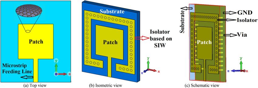
www.nature.com/scientificreports/
Figure 4. Surface current density distributions over the reference and SIW antennas at the first and second
reflection-coefficient dip frequencies in Fig. 2.
SIW loaded antenna with slots
Metasurface characteristics are introduced into the patch antenna by the inclusion of periodic array of sub-
wavelength length slots of varying length to realize a wider impedance bandwidth, as shown in Fig. 620. These slots
exposing the substrate essentially manipulate the electromagnetic (EM) response of the surface. The EM waves
impinging on the metasurface induce electric and magnetic dipole moments, which are related to the effective
permittivity and permeability of the composite medium. Detailed theoretical analysis of this type of structure
is provided in21. To confirm the antenna supports backward waves the CST Microwave Studio, which is a 3D
electromagnetic simulation tool, was used to obtain its dispersion characteristics that was computed u sing22:
1 − S11 S22 + S12 S21
βp = cos−1 (1)
2S21
where β is the wave propagation constant along the direction of propagation, and p is the length of the unit-cell.
Figure 7 shows how the phase through the structure varies with frequency. The dispersion diagram slope is
Scientific Reports | (2021) 11:10218 | https://doi.org/10.1038/s41598-021-87712-y 4
Vol:.(1234567890)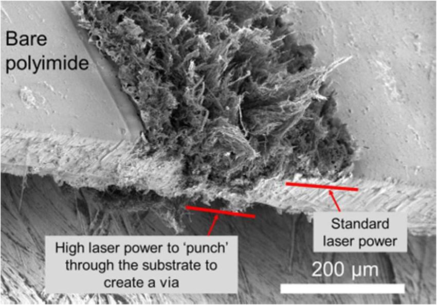
www.nature.com/scientificreports/
Figure 5. Simulated radiation gain and efficiency plots of the reference and SIW-loaded antennas.
negative between 0.1945 and 0.1951 THz. Over this frequency range the signal group and phase velocities are
oriented along opposite directions resulting in a backward wave, which is characteristic of metamaterials. This
is due to the sub-wavelength slots that control the electromagnetic response of the surface to produce a homo-
geneous response at ’macroscopic’ level. The simplified equivalent circuit of the SIW-loaded slotted antenna
in Fig. 8 will be referred to hereon as SIW-loaded MTM. The lumped element values in the equivalent circuit
were extracted using the well-established pseudo-inverse technique from S-parameters22, 23. According to22 this
structure essentially acts like MTM or composite right/left-handed (CRLH) structure. Magnitude of the equiva-
lent circuit parameters are: Lfeedline = 0.021 pH, Lpatch = 1.74186 pH, Cpatch = 0.408236 pF, RSIW = 35 Ω, LSIW = 1 pH,
LSIW-via = 2.44918 pH, & CSIW-fringe = 0.204575 pF.
The array of periodic slots etched on the patch generate multiple resonances whose frequencies can be deter-
mined from the dispersion curve when the following condition is satisfied20:
n = 0, ±1, . . . , ±(M − 1),
nπ for T - type unit - cell
βp = (2)
M n = 0, ±1, . . . , ±(M),
for π - type unit - cell
It can be shown from Eq. (2), there are three resonance frequencies which can be excited including the ±
1st-order resonances and the zeroth-order resonance at fse. These resonant frequencies are verified from the
reflection-coefficient response of the antenna in Fig. 9, which are at fr−1: 0.1941 THz, fr0: 0.1950 THz, and fr+1:
0.1957 THz. The reflection-coefficient shows significant improvement in impedance match between 0.194 and
0.196 THz with the inclusion of the slots.
The current density distribution in xy-plane at the three resonant frequencies is shown in Fig. 10. The cur-
rent distribution at fr−1: 0.1941 THz and fr+1: 0.1957 THz are very similar; however, it is significantly muted at fr0:
0.1950 THz. The size of the antenna is 3.89λ0 × 4.54λ0 × 0.08λ0 when operated at fr−1: 0.1941 THz.
Comparison of the radiation plots of the reference, SIW-loaded, and SIW-loaded slotted antennas are shown
in Fig. 11. It is evident that the SIW-loaded MTM patch antenna exhibits significantly improved performance
over the other two antennas. The optimum radiation gain of the SIW-loaded MTM antenna at resonance modes
− 1st (fr-1: 0.1941 THz), zeroth (fr0: 0.1950 THz), and + 1st (fr+1: 0.1957 THz) are 8.05 dBi @87.7°, 8.0 dBi @51.6°,
and 7.92 dBi @59.3°, respectively. Besides the gain, the radiation efficiency at resonance modes − 1st, zeroth, and
+ 1st are 45%, 45%, and 47%, respectively. In the case of fr−1: 0.1941 THz and fr+1: 0.1957 THz, the gain of the
reference antenna is comparable to the other two antennas, but this is over a very narrow azimuth range between
12° and 26°. Total dimensions of the three antennas are identical.
Scientific Reports | (2021) 11:10218 | https://doi.org/10.1038/s41598-021-87712-y 5
Vol.:(0123456789)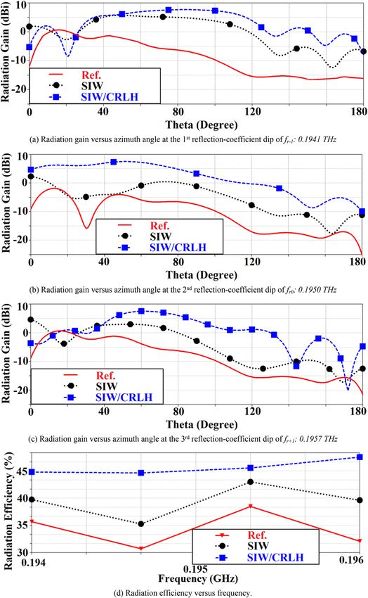
www.nature.com/scientificreports/
Figure 6. (a) front view, (b) schematic view of the SIW-loaded slotted antenna.
Figure 7. Dispersion diagram of the SIW-loaded slotted antenna.
Figure 8. The simplified equivalent circuit of the SIW-loaded slotted antenna.
Array configuration of the proposed SIW‑loaded MTM antenna for sub‑THz
applications
In this section 2 × 3 antenna arrays are realized based on the standard reference, SIW-loaded, and SIW-loaded
MTM patch antenna. The main issue encountered in an array structure is the adverse effect of mutual coupling
between the radiating elements constituting the array. Several techniques previously studied and proposed are
exemplified in23–28 but the size of the array matrix investigated in all cases reported was limited to 1 × 2. The
techniques proposed previously include the use of air gap between radiator and ground-plane or the implemen-
tation of ground-plane defection. In all cases reported the isolation achieved is limited and is restricted over
narrow frequency band.
Scientific Reports | (2021) 11:10218 | https://doi.org/10.1038/s41598-021-87712-y 6
Vol:.(1234567890)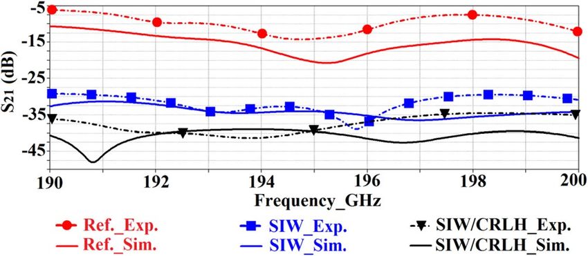
www.nature.com/scientificreports/
Figure 9. Simulated reflection-coefficient response of the reference, SIW-loaded, and SIW-loaded MTM
(CRLH) antennas.
Figure 10. Surface current density distributions over the SIW-loaded MTM antenna at the first, second and
third resonance frequencies.
In small-sized antenna array structures it is very difficult to supress the mutual coupling effects resulting
from surface wave interaction between the radiation elements due to their proximity. Proposed here is a simple
but effective mutual coupling reduction technique based on SIW isolator as described in “SIW loaded antenna
with slots” section. The prototype of the SIW-loaded MTM antenna is shown in Fig. 12, where the SIW isola-
tor is wrapped around each patch to significantly reduce propagation of surface waves and minimise substrate
loss. The prototype antenna array was coated with 500 nm thick film of Graphene. The identical patches in the
m3. The dimension of the 2 × 3 antenna array is 20 × 13.5 × 0.125 m
array have dimensions of 3 × 3 × 0.125 m m3 .
Dimensions of the optimized structural parameters are tabulated in Table 2.
Results and discussions
The simulated and measured impedance bandwidth of the standard reference, SIW-loaded, and SIW-loaded
MTM 2 × 3 antenna arrays are shown in Fig. 13. CST Microwave Studio was used obtain the simulation results.
Keysight PNA Network Analyzer with a frequency extender was used to measure the reflection-coefficient of
the antenna. These results clearly show that the SIW isolator has a significant impact on the impedance match-
ing and bandwidth of the array over the standard reference antenna array. Further improvement is achieved by
incorporating sub-wavelength slots in the patch antennas. The experimental results show that with SIW-loading
the impedance matching is improved by 10 dB on average from 190 to 200 GHz over the reference antenna
array. By incorporating both SIW-loading and sub-wavelength slots the impedance matching also improves on
average by 14 dB from 190 to 200 GHz compared to the reference array antenna. There is generally good agree-
ment between the simulated and measured results. The discrepancy in the results is attributed to manufacturing
tolerance and unaccounted loss in the simulation model.
The transmission-coefficient response of the standard reference, SIW-loaded, and SIW-loaded MTM 2 × 3
antenna array are shown in Fig. 14. These results demonstrate the effectiveness of the proposed technique of using
SIW isolator in suppressing the surface-wave propagations and reducing substrate loss to mitigate mutual cou-
pling effects without increasing the overall size of the array structure. Experimental results show that compared to
the reference antenna array the SIW-loaded array is shown to improve the isolation on average by 17 dB from 190
to 200 GHz. Also, by incorporating sub-wavelength slots the SIW-loaded MTM array is shown to suppress mutual
coupling on average by more than 28 dB across 190 GHz to 200 GHz compared to the reference array antenna.
The simulated and measured radiation gain and efficiency of the standard reference, SIW-loaded, and SIW-
loaded MTM (CRLH) array are shown in Fig. 15. Experimental results show that compared to the reference array
Scientific Reports | (2021) 11:10218 | https://doi.org/10.1038/s41598-021-87712-y 7
Vol.:(0123456789)
www.nature.com/scientificreports/

                                            Figure 11.  Simulated radiation gain and efficiency of the reference, SIW-loaded, and SIW-loaded MTM
                                            (CRLH) antennas.

                                             Parameters                                  Dimension (mm)
                                             Patch length                                3
                                             Patch width                                 3
                                             Feed line length                            2
                                             Feed line width                             0.4
                                             SIW isolator width                          0.75
                                             Number of tapered rectangular slots         5
                                             Slot lengths (sub-wavelength)               0.48, 0.56, 0.84, 1.12, 1.40
                                             Slot width                                  0.25
                                             Gap between patch and isolator              0.5
                                             Gap between feed line and isolator          0.5
                                             Diameter of vias                            0.25
                                             Gap between vias                            0.20
                                             Total length                                20
                                             Total width                                 13.5
                                             Thickness of graphene layer                 0.0005
                                             Substrate thickness                         0.125
                                             Edge-to-edge gap between adjacent patches   3.5
                                             Edge-to-edge gap between SIW isolators      1

                                            Table 2.  Structural dimensions of the antenna.

          Scientific Reports |   (2021) 11:10218 |                   https://doi.org/10.1038/s41598-021-87712-y                                    8

Vol:.(1234567890)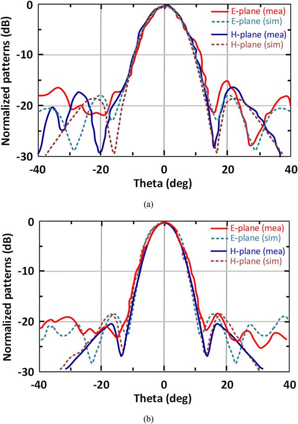
www.nature.com/scientificreports/

                                  Figure 12.  Proposed Graphene coated 2 × 3 antenna array based on SIW-loaded MTM patches, (a) isometric
                                  view, (b) front view, (c) SIW isolators framing the radiation patches, (d) back view (ground-plane), and (e–h)
                                  the fabricated antenna array prototype of the reference, SIW-loaded, SIW-loaded MTM antenna, and the
                                  ground-plane, respectively.

Scientific Reports |   (2021) 11:10218 |              https://doi.org/10.1038/s41598-021-87712-y                                                   9

                                                                                                                                            Vol.:(0123456789)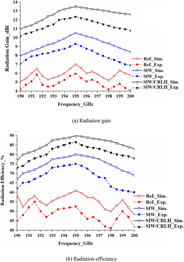
www.nature.com/scientificreports/
Figure 13. Simulated and experimental results of the reflection-coefficient of the reference, SIW-loaded, and
SIW-loaded MTM (CRLH) antenna arrays.
Figure 14. Simulated and experimental results of the transmission-coefficient ( S21) of the reference, SIW-
loaded, and SIW-loaded MTM (CRLH) antenna arrays.
Figure 15. Simulated and experimental results of the radiation gain and efficiency as a function of frequency of
the reference, SIW-loaded, and SIW-loaded MTM (CRLH) antenna arrays.
Scientific Reports | (2021) 11:10218 | https://doi.org/10.1038/s41598-021-87712-y 10
Vol:.(1234567890)www.nature.com/scientificreports/
Figure 16. Set-up to measure the array’s radiation patterns.
Figure 17. Measured and simulated radiation pattern of the 2 × 3 SIW-loaded MTM antenna arrays in E-plane
and H-plane at (a) 190 GHz, and (b) 200 GHz.
the SIW-loaded array’s gain and efficiency improve on average by 2.8 dBi and 23%, respectively, between 190 and
200 GHz. With SIW-loaded MTM the average improvement in gain and efficiency over the reference array is 6.3
dBi and 34%, respectively, between 190 and 200 GHz. These results demonstrate the array’s effective aperture is
enlarged by incorporating sub-wavelength slots, which has the benefit of not affecting the antenna’s dimensions.
The set-up to measure the far-field radiation patterns of the SIW-loaded MTM antenna arrays is shown in
Fig. 16. In transmit mode we used a 2-way power splitter in conjunction with two 3-way power splitters. It was
necessary to ensure the lengths were such that the phase at the antenna terminals were identical. This arrange-
ment was used to split equally the input sub-THz signal applied to the 2 × 3 array. Conversely, in the receive mode
we used two 3-way power combiners in combination with a 2-way power combiner. This arrangement combined
the received signal power from the 2 × 3 array. The output from the array in receive mode was connected to
Keysight E4448A spectrum analyser. Keysight E8244A signal generator was used to produce a signal that was
adjustable in the frequency range 38–40 GHz with enough power (10–20 dBm) for the mixer to generate a set of
harmonics simultaneously. The 5th harmonic was used as it was in the desired frequency range of 190–200 GHz.
Scientific Reports | (2021) 11:10218 | https://doi.org/10.1038/s41598-021-87712-y 11
Vol.:(0123456789)www.nature.com/scientificreports/
References Type Bandwidth [freq. range] Gain (dBi) Eff. (%) Size (mm3)
29 Max
Bowtie-slot 15 GHz [90–105] – 0.71 × 0.31 × 0.65
− 1.78
30 Max
Differential-fed 20 GHz [50–70] – 1.5 × 1.5 × 0.3
− 3.2
31
Ring-shaped monopole 20 GHz [50–70] Max. 0.02 Max. 35 –
32 Max
Circular open-loop 10 GHz [57–67] – 1.8 × 1.8 × 0.3
− 4.4
33
AMC embedded squared slot antenna 51 GHz [15–66] Max. 2 – 1.44 × 1.1
34
Monopole 25 GHz [45–70] Max. 4.96 – 1.953 × 1.93 × 0.25
35
Loop antenna 4 GHz [65–69] Max. 8 Max. 96.7 0.7 × 1.25
36
Dipole-antenna 7 GHz [95–102] Max. 4.8 – –
37
Tab monopole 30 GHz [45–75] Max. 0.1 Max. 42 1.5 × 1
38
Patch fed higher order mode DRA 25 GHz [330–355] Max. 7.9 Max. 74 0.2 × 0.5
39
On-chip 3D (Yagi like concept) 40 GHz [320–360] Max. 10 Max. 80 0.7 × 0.7 × 0.43
40
Half-mode cavity fed DRA 15 GHz [125–140] Max. 7.5 Max. 46 0.8 × 0.9 × 1.3
41
Slot fed stacked DRA 10 GHz [125–135] Max. 4.7 Max. 43 0.9 × 0.8 × 1.5
42
DRA 20 GHz [120–140] Max. 2.7 Max. 43 0.9 × 0.8 × 0.6
43
8 × 8 Magneto-electric dipole antenna array 14.7 GHz [130.3–145] Max. 20.5 Max. 59.2 32 × 20 × 0.818
44
4 × 1 Patch antenna array 32 GHz [259–291] Max. 5.2 – 2.47 × 1.53 × 0.675
45 2 × 1 Octagonal shorted annular ring antenna
17 GHz [303–320] Max. 4.1 Max. 38 0.55 × 0.5 × 0.3
array
This work SIW-loaded MTM 10 GHz [190–200] Max. 12.2 Max. 86 20 × 13.5 × 0.125
Table 3. Salient features of the proposed SIW-loaded MTM antenna array compared with recent publications.
At the receiver, the received signal is mixed with signal from Keysight E8244A with a frequency which was offset
from the transmitter local oscillator, and this offset frequency (ΔFIF) determines the system harmonic number,
which is used (5ΔFIF). The simulated and measured patterns of the 2 × 3 SIW-loaded MTM antenna arrays in
the E- and H-planes at 190 GHz and 200 GHz are shown in Fig. 17. CST Microwave Studio was used obtain
the simulation results. The measured results agree well with the simulations. The radiation pattern is stable and
symmetrical within the operating band of the array. Due to the unpredictable reflection from the fixtures and
measurement setup near the antenna under test, a series of small ripples can be seen in the measured results.
Performance parameters of the proposed SIW-loaded MTM antenna array is compared with other recently
published millimeter-wave and sub-THz antennas in Table 3. The comparison shows that the proposed antenna
array has comparable gain and radiation efficiency to the cited references, which confirm the effectiveness of the
proposed approach. It is less complex and cost effective to implement and realize in practice for mass production,
which makes it a viable candidate for applications to sub-terahertz wireless systems.
Conclusion
We have demonstrated the use of a Graphene-based antenna at sub-THz and the effectiveness of the proposed
technique of framing each radiator with SIW. This technique is shown here to reduce surface wave propaga-
tions and suppressing near-field mutual coupling between the radiators in an array. The consequence of this is
significant improvement in the array’s performance in terms of impedance matching and radiation performance
which is achieved without compromising the footprint of the antenna array. Further improvement in performance
was demonstrated by incorporating sub-wavelength slots in the patch radiators. The feed mechanism employed
is however considered to be unfeasible for a large array, where aperture coupling would be more appropriate.
Received: 30 November 2020; Accepted: 1 April 2021
References
1. Nagatsuma, T., Ducournau, G. & Renaud, C. C. Advances in terahertz communications accelerated by photonics. Nat. Photonics
10, 371–379 (2016).
2. Akyildiz, I. F., Jornet, J. M. & Han, C. Terahertz band: Next frontier for wireless communications. Physical Communication 12,
16–32 (2014).
3. Song, H. J. & Nagatsuma, T. Present and future of terahertz communications. IEEE Trans. Terahertz Sci. Technol. 1, 256–263 (2011).
4. Al Hadi, R. et al. A 1 k-pixel video camera for 0.7–1.1 terahertz imaging applications in 65-nm CMOS. IEEE J. Solid-State Circuits
47, 2999–3012 (2012).
5. Walther, M. et al. Terahertz conductivity of thin gold films at the metal-insulator percolation transition. Phys. Rev. B 76, 125408
(2007).
6. Hanson, G. Radiation efficiency of nano-radius dipole antennas in the microwave and far-infrared regimes. IEEE Antennas Propag.
Mag. 50, 66–77 (2008).
7. Laman, N. & Grischkowsky, D. Terahertz conductivity of thin metal films. Appl. Phys. Lett. 93, 051105 (2008).
8. Kuan, T., Inoki, C., Oehrlein, G., Rose, K., Zhao, Y. P., Wang, G. C. et al. Fabrication and performance limits of sub-0.1 µm Cu
interconnects. In MRS Proceedings (2000).
Scientific Reports | (2021) 11:10218 | https://doi.org/10.1038/s41598-021-87712-y 12
Vol:.(1234567890)www.nature.com/scientificreports/
9. Lee, D.-K. et al. Highly sensitive and selective sugar detection by terahertz nano-antennas. Sci. Rep. 5, 15459 (2015).
10. Razzari, L. et al. Terahertz dipole nanoantenna arrays: resonance characteristics. Plasmonics 8, 133–138 (2013).
11. Feuillet-Palma, C., Todorov, Y., Vasanelli, A. & Sirtori, C. Strong near field enhancement in THz nano-antenna arrays. Sci. Rep. 3,
1361 (2013).
12. Lier, E., Werner, D. H., Scarborough, C. P., Wu, Q. & Bossard, J. A. An octave-bandwidth negligible-loss radio frequency metamate-
rial. Nat. Mater. 10, 216–222 (2011).
13. Pfeiffer, U. R. et al. Current status of terahertz integrated circuits: from components to systems. In IEEE BiCMOS and Compound
Semiconductor Integrated Circuits and Technology Symposium (BCICTS), 107 (2018).
14. Dan, I. et al. A Terahertz wireless communication link using a superheterodyne approach. IEEE Trans. Terahertz Sci. Technol.
10(1), 1–12 (2020).
15. Pendry, J. B., Martin-Moreno, L. & GarciaVidal, F. J. Mimicking surface plasmons with structured surfaces. Science 305, 847–848
(2004).
16. Shimada, Y., Iida, H. & Kinoshita, M. Recent research trends of terahertz measurement standards. IEEE Trans. Terahertz Sci.
Technol. 5(6), 1166–1172 (2015).
17. Bozzi, M., Pierantoni, L. & Bellucci, S. Applications of graphene at microwave frequencies. Radioengineering 24(3), 661–669 (2015).
18. Yin, Y., Yao, Y., Liu, X., Qi, L., Chen, Z., Yu, J., & Chen, X. Research on terahertz reflectarray based on graphene surface and PET
substrate. In 10th UK-Europe-China Workshop on Millimetre Waves and Terahertz Technologies (UCMMT), 1–3 (2017).
19. Zhao et al., "Replacing the metal electrodes in triboelectric nanogenerators: High-performance laser-induced graphene electrodes",
Nano Energy, 75, 104958 (2020).
20. Finch, M. F. & Lail, B. A. Multi-coupled resonant splitting with a nano-slot metasurface and PMMA phonons. In Proc. SPIE 9547,
Plasmonics: Metallic Nanostructures and Their Optical Properties XIII, 954710, 28, 1–6 (2015).
21. Martini, E., Mencagli, M. Jr. & Maci, S. Metasurface transformation for surface wave control. Philos. Trans. R. Soc. A 373, 20140355
(2015).
22. Caloz, C. & Itoh, T. Electromagnetic Metamaterials: Transmission Line Theory and Microwave Applications (Wiley, 2005).
23. Kou, N., Shi, Y. & Li, L. New equivalent circuit analysis and synthesis for broadband composite right/left-handed transmission
line metamaterials. ACES J. 31(8), 884–893 (2016).
24. Farsi, S., Schreurs, D. & Nauwelaers, B. Mutual coupling reduction of planar antenna by using a simple microstrip U-section. IEEE
Ant. Wirel. Propag. Lett. 11, 1501–1503 (2012).
25. Alsath, M. G., Kanagasabai, M. & Balasubramanian, B. Implementation of slotted meander line resonators for isolation enhance-
ment in microstrip patch antenna arrays. IEEE Antennas Wirel. Propag. Lett. 12, 15–18 (2013).
26. Shafique, M. F., Qamar, Z., Riaz, L., Saleem, R. & Khan, S. A. Coupling suppression in densely packed microstrip arrays using
metamaterial structure. Microw. Opt. Technol. Lett. 57(3), 759–763 (2015).
27. Ghosh, J., Ghosal, S., Mitra, D. & Chaudhuri, S. R. B. Mutual coupling reduction between closely placed microstrip patch antenna
using meander line resonator. Progress in Electromag. Research Lett. 59, 115–122 (2016).
28. Yang, Xu., Liu, Y., Yun-Xue, Xu. & Gong, S.-X. Isolation enhancement in patch antenna array with fractal UC-EBG structure and
cross slot. IEEE Antennas Wirel. Propag. Lett. 16, 2175–2178 (2017).
29. Khan, M. S., Tahir, F. A. & Cheema, H. M. Design of bowtie-slot on-chip antenna backed with E-shaped FSS at 94 GHz. In 10th
European Conference on Antennas and Propagation (EuCAP), Davos, 1–3 (2016).
30. Wang, L. & Sun, W. Z. A 60-GHz differential-fed circularly polarized on-chip antenna based on 0.18-μm COMS technology with
AMC structure. In IET International Radar Conference, Hangzhou, 1–4 (2015).
31. Huang, H. T., Yuan, B., Zhang, X. H., Hu, Z. F. & Luo, G. Q. A circular ring-shape monopole on-chip antenna with artificial mag-
netic conductor. In Asia-Pacific Microwave Conference (APMC), Nanjing, 1–3 (2015).
32. Bao, X., Guo, Y. & Xiong, Y. 60-GHz AMC-based circularly polarized on-chip antenna using standard 0.18-μm CMOS Technology.
IEEE Trans. Antennas Propag. 60(5), 2234–2241 (2012).
33. Lin, F. & Ooi, B. L. Integrated millimeter-wave on-chip antenna design employing artificial magnetic conductor. In IEEE Interna-
tional Symposium on Radio-Frequency Integration Technology (RFIT), Singapore, 174–177 (2009).
34. Upadhyay, S. & Srivastava, S. A 60-GHz on-chip monopole antenna using silicon technology. In IEEE Applied Electromagnetics
Conference (AEMC), Bhubaneswar, 1–2 (2013).
35. Song, Y., Wu, Y., Yang, J. & Kang, K. The design of a high gain on-chip antenna for SoC application. In IEEE MTT-S International
Microwave Workshop Series on Advanced Materials and Processes for RF and THz Applications (IMWS-AMP), Suzhou, 1–3 (2015).
36. Nafe, M., Syed, A. & Shamim, A. Gain enhancement of low profile on-chip dipole antenna via artificial magnetic conductor at 94
GHz. In 9th European Conference on Antennas and Propagation (EuCAP), Lisbon, 1–3 (2015).
37. Yang, W., Ma, K., Yeo, K. S. & Lim, W. M. A 60 GHz on-chip antenna in standard CMOS silicon technology. In IEEE Asia Pacific
Conference on Circuits and Systems, Kaohsiung, 252–255 (2012).
38. Li, C. & Chiu, T. 340-GHz low-cost and high-gain on-chip higher order mode dielectric resonator antenna for THz applications.
IEEE Trans. Terahertz Sci. Technol. 7(3), 284–294 (2017).
39. Deng, X., Li, Y., Liu, C., Wu, W. & Xiong, Y. 340 GHz on-chip 3-D antenna with 10 dBi gain and 80% radiation efficiency. IEEE
Trans. Terahertz Sci. Technol. 5(4), 619–627 (2015).
40. Hou, D. et al. D-band on-chip higher-order-mode dielectric-resonator antennas fed by half-mode cavity in CMOS technology.
IEEE Antennas Propag. Mag. 56(3), 80–89 (2014).
41. Hou, D. et al. 130-GHz on-chip meander slot antennas with stacked dielectric resonators in standard CMOS technology. IEEE
Trans. Antennas Propag. 60(9), 4102–4109 (2012).
42. Hou, D. et al. Silicon based on-chip antenna design for millimeter-wave/THz application. In Elect. Design of Adv. Pkg. and Syst.
Symp (EDAPS), 1–4 (2011).
43. Li, X., Xiao, J., Qi, Z., & Zhu, H. Broadband and high-gain millimeter-wave and terahertz antenna arrays. In Int. Conference on
Microwave and Millimeter Wave Technology (ICMMT), 1–3 (2019).
44. Benakaprasad, B., Eblabla, A., Li, X., Thayne, I., Wallis, D. J., Guiney, I., Humphreys, C. & Elgaid, K. Terahertz monolithic integrated
circuits (TMICs) array antenna technology on GaN-on-low resistivity silicon substrates. In 41st Int. Conference on Infrared, Mil-
limeter, and Terahertz waves (IRMMW-THz), 1–2 (2016).
45. Zhu, H., Li, X., Qi, Z. & Xiao, J. A 320 GHz octagonal shorted annular ring on-chip antenna array. IEEE Access 8, 84282–84289
(2020).
Acknowledgements
This work was supported in part by the Ministerio de Ciencia, Innovación y Universidades, Gobierno de España
(MCIU/AEI/FEDER, UE) under Grant RTI2018-095499-B-C31, in part by the Innovation Programme under
Grant H2020-MSCA-ITN-2016 SECRET-722424, and in part by the U.K. Engineering and Physical Sciences
Research Council (EPSRC) under Grant EP/E022936/1.
Scientific Reports | (2021) 11:10218 | https://doi.org/10.1038/s41598-021-87712-y 13
Vol.:(0123456789)www.nature.com/scientificreports/
Author contributions
Conceptualization, M.A., B.S.V., S.A., C.H.S., R.A.-A., I.H., F.F., and E.L.; methodology, M.A., B.S.V., S.A., C.H.S.,
N.S., S.J.F., A.A.A., R.A.-A., I.H., F.F., and E.L.; software, M.A., B.S.V., S.S., C.H.S., R.A.-A., I.H., and J.A.M.;
validation, M.A., B.S.V., S.S., S.A., C.H.S., N.S., S.J.F., A.A.A., R.A.-A., I.H., J.A.M., F.F., and E.L.; formal analy-
sis, M.A., B.S.V., S.A., C.H.S., S.J.F., A.A.A., R.A.-A., I.H., J.A.M., F.F., and E.L.; investigation, M.A., B.S.V., S.A.,
C.H.S., R.A.-A., I.H., J.A.M., F.F., and E.L.; resources, M.A., B.S.V., S.S., S.A., C.H.S., N.S., S.J.F., A.A.A., R.A.-A.,
I.H., J.A.M., F.F., and E.L.; data curation, M.A., B.S.V., S.S., S.A., C.H.S., N.S., S.J.F., J.A.M., F.F., and E.L.; writ-
ing—original draft preparation, M.A.; writing—review and editing, M.A., B.S.V., S.S., S.A., C.H.S., N.S., S.J.F.,
A.A.A., R.A.-A., I.H., J.A.M., F.F., and E.L.; visualization, M.A., B.S.V., S.A., C.H.S., N.S., R.A.-A., I.H., F.F., and
E.L.; supervision, E.L.; project administration, R.A.-A., F.F., and E.L.; funding acquisition, R.A.-A., F.F., and E.L.
Competing interests
The authors declare no competing interests.
Additional information
Correspondence and requests for materials should be addressed to M.A.
Reprints and permissions information is available at www.nature.com/reprints.
Publisher’s note Springer Nature remains neutral with regard to jurisdictional claims in published maps and
institutional affiliations.
Open Access This article is licensed under a Creative Commons Attribution 4.0 International
License, which permits use, sharing, adaptation, distribution and reproduction in any medium or
format, as long as you give appropriate credit to the original author(s) and the source, provide a link to the
Creative Commons licence, and indicate if changes were made. The images or other third party material in this
article are included in the article’s Creative Commons licence, unless indicated otherwise in a credit line to the
material. If material is not included in the article’s Creative Commons licence and your intended use is not
permitted by statutory regulation or exceeds the permitted use, you will need to obtain permission directly from
the copyright holder. To view a copy of this licence, visit http://creativecommons.org/licenses/by/4.0/.
© The Author(s) 2021
Scientific Reports | (2021) 11:10218 | https://doi.org/10.1038/s41598-021-87712-y 14
Vol:.(1234567890)You can also read