Atomic-scale quantification of charge densities in two-dimensional materials
←
→
Page content transcription
If your browser does not render page correctly, please read the page content below
PHYSICAL REVIEW B 98, 121408(R) (2018)
 Rapid Communications

                  Atomic-scale quantification of charge densities in two-dimensional materials

        Knut Müller-Caspary,1,2,3,* Martial Duchamp,3,4 Malte Rösner,5,6,7 Vadim Migunov,3 Florian Winkler,3 Hao Yang,7
                  Martin Huth,8 Robert Ritz,8 Martin Simson,8 Sebastian Ihle,8 Heike Soltau,8 Tim Wehling,5,6
                            Rafal E. Dunin-Borkowski,3 Sandra Van Aert,1 and Andreas Rosenauer2
                            1
                               EMAT, Universiteit Antwerpen, Groenenborgerlaan 171, B-2020 Antwerpen, Belgium
                                     2
                                       IFP, Universität Bremen, Otto-Hahn-Allee 1, 28359 Bremen, Germany
                       3
                         Ernst Ruska-Centre for Microscopy and Spectroscopy with Electrons and Peter Grünberg Institute,
                                                Forschungszentrum Jülich, 52425 Jülich, Germany
     4
       School of Materials Science and Engineering, Nanyang Technological University, 50 Nanyang Avenue, Singapore 639798, Singapore
                                     5
                                       ITP, Universität Bremen, Otto-Hahn-Allee 1, 28359 Bremen, Germany
                                     6
                                       BCCMS, Universität Bremen, Am Fallturm 1, 28359 Bremen, Germany
              7
                Department of Physics and Astronomy, University of Southern California, Los Angeles, California 90089-0484, USA
                                        8
                                          PNDetector GmbH, Otto-Hahn-Ring 6, 81739 München, Germany

                                              (Received 9 May 2018; published 24 September 2018)

                   The charge density is among the most fundamental solid state properties determining bonding, electrical
                characteristics, and adsorption or catalysis at surfaces. While atomic-scale charge densities have as yet been
                retrieved by solid state theory, we demonstrate both charge density and electric field mapping across a
                mono-/bilayer boundary in 2D MoS2 by momentum-resolved scanning transmission electron microscopy. Based
                on consistency of the four-dimensional experimental data, statistical parameter estimation and dynamical
                electron scattering simulations using strain-relaxed supercells, we are able to identify an AA-type bilayer
                stacking and charge depletion at the Mo-terminated layer edge.

                DOI: 10.1103/PhysRevB.98.121408

    The discovery that mechanical, thermal, optical, and elec-           diffraction patterns for a probe scanning a 2D raster, which
trical properties of 2D materials such as graphene, Xenes                requires current ultrafast cameras [10–14] being capable of
(silicene, germanene), or transition metal dichalcogenides               submillisecond frame times.
(TMDs, e.g., MoS2 , WSe2 ) drastically differ from their bulk                The physical background of our approach is summarized
counterparts evoked enormous attention of both fundamental               schematically in Fig. 1. The wave function of the incident
and applied research. The dominant route to get an atom-                 STEM probe, 0 , with amplitude (black) and phase (red)
istic understanding of bonding, conductance, band gaps, or               suffers a phase shift exp(iσ VP ) by interacting with the pro-
photoluminescence spectra currently consists of setting up               jected Coulomb potential VP , σ = 0.01 (V nm)−1 being the
a structural model and performing ab initio simulations of               interaction constant. Because the projected electric field EP =
the charge density, typically involving density functional the-          −∇VP is not constant at the scale of the probe, the phase of
ory [1–3] (DFT). Experimentally, electron microscopy can                 the scattered wave is now curved. The deflection is measured
be used to provide atomically resolved structural data, e.g.,            in terms of the average lateral momentum transfer p⊥  from
by conventional scanning transmission electron microscopy                the first moment in diffraction patterns [7] with ⊥ indexing
(STEM) imaging at a spatial resolution down to 50 pm.                    a plane perpendicular to the optical axis. Within the phase
However, an ultimate goal would be the direct observation                approximation, being valid for thin specimen, and accounting
of charge densities and electric fields at atomic resolution by          for partial spatial coherence of the electron source, p⊥  can
electron microscopy at reasonable fields of view. Here, we               be related to the projected electric field EP by Ehrenfest’s
take an important step towards this challenge by mapping                 theorem which results in [15]
these fundamental physical properties in 2D MoS2 at atomic
scale with a precision that allows for conclusions on, e.g.,                            v = [w ◦ (EP ∗ I0 )](R)
                                                                                 p⊥ (R)                          =: Em (R).
                                                                                                                                      (1)
                                                                                           −e
bilayer stacking.
    This is now feasible as differential phase contrast                  Here, R is the scan position, w describes the partial coherence
[4–6] (DPC) STEM currently undergoes a rapid development                 of the electron source (typically Gaussian), I0 equals the
from a classical, qualitative approach to quantitative electron          normalized intensity of the incident probe, −e is the electron
picodiffraction [7,8] based on first moment detection [9]. The           charge, and v its velocity. The measured electric field, Em , is
enhancement involves the acquisition of momentum-resolved                thus directly proportional to the momentum transfer and rep-
STEM data, i.e., a 4D data set obtained by recording 2D                  resents the actual projected field EP , convolved (∗) with the
                                                                         probe intensity I0 and cross correlated (◦) with the source w.
                                                                         Note that these parameters determine the general lower limit
 *
     Corresponding author: k.mueller-caspary@fz-juelich.de               for the spatial resolution in STEM. Furthermore, the measured

2469-9950/2018/98(12)/121408(5)                                   121408-1                                ©2018 American Physical Society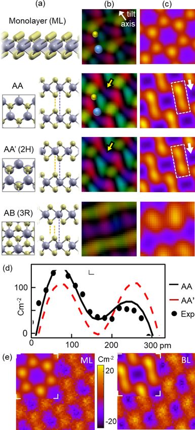
KNUT MÜLLER-CASPARY et al. PHYSICAL REVIEW B 98, 121408(R) (2018)
FIG. 1. Atomic electric field measurement. (a) Interaction of
an electron wave (amplitude: black, phase: red) with the projected
potential VP and electric field EP of an atom. (b) Ronchigram
acquired with 250 μs frame time near a Mo site. The number of
detected electrons is color coded. (c) Momentum transfer (red) and
projected electric field Em (blue) determined from the Ronchigram
in (c).
charge density ρm is obtained from Maxwell’s equations,
= ε0 div⊥ Em (R)
ρm (R) = [w ◦ (ρP ∗ I0 )](R),
(2)
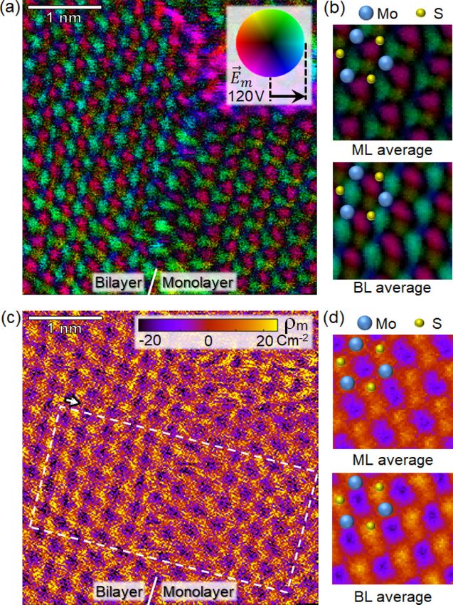
and quantifies the projected charge density with the spatial FIG. 2. Measured electric field and charge density in MoS2 .
resolution corresponding to the ultimate limit set by the of a mono-/bilayer (ML/BL)
(a) Color-coded electric field Em (R)
boundary with (b) unit cell averages. (c) Charge density ρm (R)
microscope [15].
We used the pnCCD [10,14] camera with a frame rate calculated from (a) using Eq. (2) with the line profile region for
of 4 kHz to record the central parts of the diffraction pat- Fig. 4(b) indicated (dashed rectangle). (d) Unit cell averages from (c).
terns (Ronchigrams) on a 2562 STEM raster employing an
aberration-corrected STEM instrument operated at 80 kV to was calculated from Fig. 2(a) with ML and BL averages in
avoid specimen damage [15]. Figure 1(b) depicts an example Fig. 2(d). In both the ML and the BL we observe the peri-
Ronchigram recorded close to a Mo atom. Although the odicity of the hexagonal MoS2 lattice and individual atomic
electron fluence was kept low at approximately 5.5 × 10⁵ sites in Figs. 2(c) and 2(d). Note that the measured electric
2
electrons/Å , the redistribution of intensity due to the atomic field vanishes at atomic sites as seen from the structural model
electric field is obvious. Its first moment yields the momentum imposed on the averaged cells in Fig. 2(b). This is reasonable
transfer p⊥ depicted in red in Fig. 1(c) with a modulus of because the measured field involves the convolution of the
0.18h nm−1 . This corresponds to the measured electric field projected electric field EP with the probe intensity I0 [7].
Em (blue) with a magnitude of 114 V calculated using Eq. (1). Interestingly the electric fields in the ML and the BL look
The momentum is given in units of Planck’s constant h and very similar concerning their shape as can be inferred from
the measured electric field in volts as it involves a projection the color sequence around an atom, but the field magnitudes
operation through EP , according to Eq. (1). in the BL are higher. This points at a double-monolayer-type
Figure 2(a) depicts the atomically resolved electric field stacking referred to as AA [19] or 3R-like [20], as investigated
Em measured across an area of 4 × 4 nm. This region is below. The ML/BL edge region shows a different field distri-
of particular interest because it contains a mono-/bilayer bution which is indicative for a particular edge termination
(ML/BL) boundary, as will be confirmed by simulations determined hereafter. As to the charge density in Figs. 2(c)
below. It is furthermore consistent with atom counting results and 2(d) we find positive values at atomic sites owing to
using a statistics-based method [16–18] to evaluate scattering the (screened) nuclear charge surrounded by negative values
cross sections [15]. because of the electronic contributions. In the boundary region
Field averages from the ML and BL have been calculated the charge density variations appear weaker than in the ML or
by a unit cell segmentation of the data and subsequent averag- BL. We emphasize that both electric field and charge density
ing involving a geometric transform as to the average cell ge- are mapped directly, without input of structure or chemistry,
ometry. The results are depicted in Fig. 2(b) with atomic sites in contrast to former studies [21–23]. Furthermore no complex
indicated. Using Eq. (2), the charge density ρm in Fig. 2(c) reconstruction procedure is involved such as for ptychography
121408-2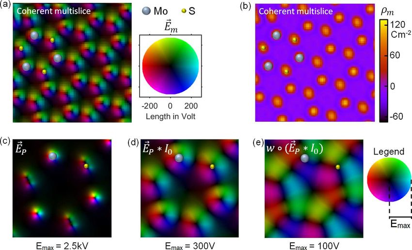
ATOMIC-SCALE QUANTIFICATION OF CHARGE …                                                      PHYSICAL REVIEW B 98, 121408(R) (2018)

[24,25], and no field-free area for a reference wave is needed
as is the case for holography [26].
   The data of Fig. 2 is now investigated in more detail to
explore whether the precision of our charge density mapping
allows us to draw conclusions about the stacking sequence
of the BL and the termination at the ML/BL edge, solely
from the charge density results. To this end, supercells with
different stacking sequences and edge terminations have been
created, strain relaxed by DFT [2,3] and then used as an input
for STEM multislice [27] simulations particularly accounting
for partial spatial coherence and specimen tilt. The analysis of
the stacking is presented in Fig. 3 with the different stacking
configurations illustrated in (a), simulated electric fields in (b),
and charge densities in (c). Added as a plausibility check, the
ML simulation in Fig. 3 (top) is in remarkable quantitative
agreement with its experimental counterparts in Figs. 2(b)
and 2(d), bearing in mind that the color scales of Figs. 2
and 3 are identical. Note that the actual specimen tilt of 7.5◦
around the axis indicated in (b), top, was accounted for [15].
The stacking terminology was adopted from Ref. [19] with the
Ramsdell notation in brackets where applicable.
   The AB sequence for the BL stacking can immediately
be rejected by comparison with Figs. 2(b) and 2(d). Distin-
guishing between AA and AA is more challenging when
considering only the electric fields. A more obvious decision
is made from the charge densities in Fig. 3(c) of which the
AA variant exhibits an asymmetric dumbbell similar to the ex-
periment in Fig. 2(d) but contrary to the AA stacking. The
asymmetry becomes clear from the structural model since all
atomic columns will have identical projected potentials for
the AA case. To illustrate this explicitly, Fig. 3(d) shows the
integrated charge density profiles across the dumbbell marked
by the dashed rectangles in Fig. 3(c). Indeed the AA stack-
ing model represents the experimental data best concerning
both the asymmetric character and the magnitude. Finally,
Fig. 3(e) compiles simulation and experiment for both the ML
and the AA-stacked BL at the same color scale, exhibiting
perfect agreement within the experimental precision imposed
by counting statistics.
   The violation of inversion symmetry as seen from the pro-
jected charge density for the BL has important consequences
on the optical properties. Since the AA-stacked bilayer can be
considered a double monolayer, it exhibits twice the nonlinear
susceptibility compared to a ML and shows strong spin- and
valley selective circular dichroism [20]. However, the AA
stacking is one variant among several others that have been
observed, each constituting a local energetic minimum and                  FIG. 3. Simulated electric fields and charge densities. (a) Models
unique optical properties [19,20,28]. That the present BL can          for the monolayer (ML) and bilayer stackings. (b) Electric field
take a stacking sequence that does not correspond to the global        corresponding to (a) with distinguishing features marked by the
energetic minimum can be explained by the mechanical stress            yellow arrow. A tilt of 7.5◦ around the axis indicated [(b), top]
introduced during exfoliation and by the fact that the BL flake        was determined from the experimental data. (c) Charge densities
is kept fixed by surrounding (multi)layer steps or amorphous           derived from (b). Color legends of (b) and (c) are equal to Fig. 2.
contamination.                                                         (d) Integrated charge density profiles taken in (c) (dashed rectangle)
                                                                       and the equivalent region in Fig. 2(d). (e) Simulation (insets) and unit
   Concerning the termination of the BL edge, Fig. 4(a) shows
                                                                       cell averages superimposed for the ML and the AA-stacked BL.
the sulfur dimer (S2 ), sulfur monomer (S1 ), and molybde-
num monomer (Mo1 ) configurations. The differences become
most obvious in average charge density profiles across the             in the ML are observed as shown at the top of Fig. 4(b).
ML/BL boundary calculated in the region indicated by the               Interestingly, it drops to [−4.5 . . . 3] cm−2 at the edge. The
dashed rectangle in Fig. 2(c). Experimentally, a charge density        three simulated counterparts drawn at the bottom of Fig. 4(b)
oscillation of up to ±9 cm−2 in the BL and ±6.5 cm−2                   have been obtained by STEM multislice [27] simulations

                                                                 121408-3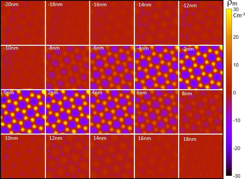
KNUT MÜLLER-CASPARY et al.                                                                 PHYSICAL REVIEW B 98, 121408(R) (2018)

                                                                       ever, simulation and experiment match nearly perfectly safely
                                                                       inside the ML/BL, while the Mo1 simulation exhibits still
                                                                       slightly too high charge densities near the edge. This might
                                                                       be attributed to strain which is not taken into account in the
                                                                       simulation. In terms of Pythagorean sums of the differences
                                                                       to the experimental profile per pixel, we find 0.031, 0.024,
                                                                       and 0.021 cm−2 for the S2 , S1 , and Mo1 cases, respectively, so
                                                                       that the Mo termination is the most likely edge configuration.
                                                                       This demonstrates that this technique can be very valuable in
                                                                       future studies where the charge density is to be correlated, e.g.,
                                                                       with catalytic or electrical properties. For example, Mo edges
                                                                       were found catalytically active [29,30] and exhibit metallic
                                                                       character [31] aside from the semiconducting nature of MoS2 .
                                                                           To conclude, distinguishing features of an AA-stacked
                                                                       MoS2 bilayer could be resolved by means of atomic-scale
                                                                       electric field and charge density mapping, which exhibit a
                                                                       violation of inversion symmetry. The assignment of a Mo
                                                                       termination to the mono-/bilayer edge, accompanied by a
                                                                       depleted charge density, demonstrates the sensitivity of the
                                                                       method. The presented study shows great promise to shed
                                                                       light on the atomic-scale electrical configuration of vacancies,
                                                                       dopant atoms, dislocations, stacking faults, and multilayer
                                                                       stacking in the growing family of 2D materials. Enhancing the
                                                                       precision further so as to be sensitive to bonding effects will
                                                                       surely dominate upcoming work, for which low-Z 2D mate-
                                                                       rials such as N-doped graphene or BN would be interesting
                                                                       applications.
                                                                           This concurrence of excellent momentum resolution, the
                                                                       quantum mechanical interpretation of 4D experimental data,
   FIG. 4. Termination of the MoS2 ML/BL edge. (a) Strain-
                                                                       aberration-corrected low-voltage STEM, and ultrafast elec-
minimized edge models used for the multislice simulations.
                                                                       tron detectors is fundamentally changing the scope of atomic-
(b) Experimental (top) charge density profile taken in the dashed
region of Fig. 2(c). Below the simulated analogons are shown for
                                                                       resolution solid state research, now allowing for atomic-scale
the models in (a), indicating a Mo1 termination.                       charge density mapping without any prior knowledge of
                                                                       atomic species or sites.

                                                                          K.M.-C. acknowledges funding from the Initiative and
using the experimental parameters and the structures from              Network Fund of the Helmholtz Association (VH-NG-1317)
Fig. 4(a). The measured charge depletion is only observed              within the framework of the Helmholtz Young Investigator
for an edge terminated by a Mo monomer (black). How-                   Group moreSTEM at Forschungszentrum Jülich, Germany.

 [1] P. Blaha, K. Schwarz, P. Sorantin, and S. Trickey, Comput.        [10] K. Müller, H. Ryll, I. Ordavo, S. Ihle, L. Strüder, K. Volz, J.
     Phys. Commun. 59, 399 (1990).                                          Zweck, H. Soltau, and A. Rosenauer, Appl. Phys. Lett. 101,
 [2] G. Kresse and J. Furthmüller, Comput. Mater. Sci. 6, 15 (1996).        212110 (2012).
 [3] G. Kresse and J. Hafner, Phys. Rev. B 47, 558 (1993).             [11] V. B. Ozdol, C. Gammer, X. G. Jin, P. Ercius, C. Ophus, J.
 [4] N. H. Dekkers and H. de Lang, Optik 41, 452 (1974).                    Ciston, and A. M. Minor, Appl. Phys. Lett. 106, 253107 (2015).
 [5] H. Rose, Ultramicroscopy 2, 251 (1977).                           [12] K. Müller-Caspary, A. Oelsner, and P. Potapov, Appl. Phys.
 [6] N. Shibata, S. D. Findlay, Y. Kohno, H. Sawada, Y. Kondo, and          Lett. 107, 072110 (2015).
     Y. Ikuhara, Nat. Phys. 8, 611 (2012).                             [13] M. W. Tate, P. Purohit, D. Chamberlain, K. X. Nguyen, R.
 [7] K. Müller, F. F. Krause, A. Beche, M. Schowalter, V. Galioit,          Hovden, C. S. Chang, P. Deb, E. Turgut, J. T. Heron, D. G.
     S. Löffler, J. Verbeeck, J. Zweck, P. Schattschneider, and A.          Schlom, D. C. Ralph, G. D. Fuchs, K. S. Shanks, H. T. Philipp,
     Rosenauer, Nat. Commun. 5, 5653 (2014).                                D. A. Muller, and S. M. Gruner, Microscopy and Microanalysis
 [8] K. Müller-Caspary, F. F. Krause, T. Grieb, S. Löffler,                 22, 237 (2016).
     M. Schowalter, A. Béché, V. Galioit, D. Marquardt, J.             [14] H. Ryll, M. Simson, R. Hartmann, P. Holl, M. Huth, S. Ihle, Y.
     Zweck, P. Schattschneider, J. Verbeeck, and A. Rosenauer,              Kondo, P. Kotula, A. Liebel, K. Müller-Caspary, A. Rosenauer,
     Ultramicroscopy 178, 62 (2017).                                        R. Sagawa, J. Schmidt, H. Soltau, and L. Strüder, J. Instrum.
 [9] E. M. Waddell and J. N. Chapman, Optik 54, 83 (1979).                  11, P04006 (2016).

                                                                 121408-4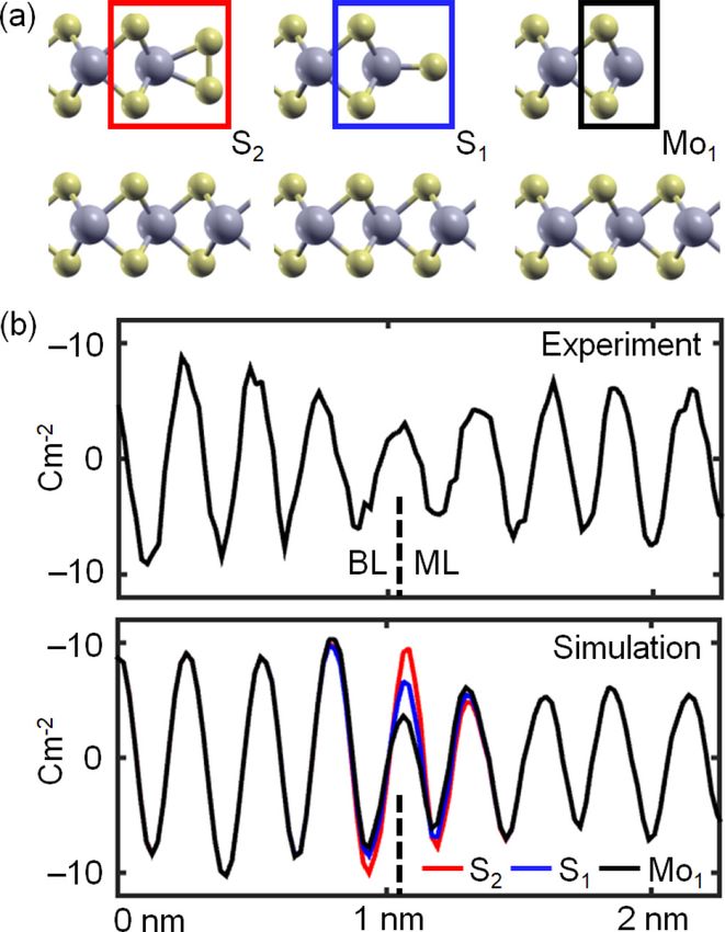
ATOMIC-SCALE QUANTIFICATION OF CHARGE …                                                         PHYSICAL REVIEW B 98, 121408(R) (2018)

[15] See Supplemental Material at http://link.aps.org/supplemental/             U. Starke, J. H. Smet, and U. Kaiser, Nat. Mater. 10, 209
     10.1103/PhysRevB.98.121408 for the mathematical treatment                  (2011).
     of partial spatial coherence, experimental and simulation de-       [24]   H. Yang, R. N. Rutte, L. Jones, M. Simson, R. Sagawa, H. Ryll,
     tails, simulation studies of focus dependence, spatial coherence,          M. Huth, T. J. Pennycook, M. L. H. Green, H. Soltau, Y. Kondo,
     and the validity of the phase approximation.                               B. G. Davis, and P. D. Nellist, Nat. Commun. 7, 12532 (2016).
[16] S. Van Aert, K. J. Batenburg, M. D. Rossell, R. Erni, and G. Van    [25]   S. Gao, P. Wang, F. Zhang, G. T. Martinez, P. D. Nellist, X. Pan,
     Tendeloo, Nature (London) 470, 374 (2011).                                 and A. I. Kirkland, Nat. Commun. 8, 163 (2017).
[17] S. Van Aert, A. De Backer, G. T. Martinez, B. Goris, S. Bals,       [26]   P. A. Midgley and R.-E. Dunin-Borkowski, Nat. Mater. 8, 271
     G. Van Tendeloo, and A. Rosenauer, Phys. Rev. B 87, 064107                 (2009).
     (2013).                                                             [27]   A. Rosenauer and M. Schowalter, in Springer Proceedings in
[18] A. D. Backer, K. van den Bos, W. V. den Broek, J. Sijbers, and             Physics, edited by A. G. Cullis and P. A. Midgley (Springer,
     S. V. Aert, Ultramicroscopy 171, 104 (2016).                               Dordrecht, 2007), Vol. 120, pp. 169–172.
[19] J. He, K. Hummer, and C. Franchini, Phys. Rev. B 89, 075409         [28]   M. Xia, B. Li, K. Yin, G. Capellini, G. Niu, Y. Gong, W. Zhou,
     (2014).                                                                    P. M. Ajayan, and Y.-H. Xie, ACS Nano 9, 12246 (2015).
[20] T. Jiang, H. Liu, D. Huang, S. Zhang, Y. Li, X. Gong,               [29]   C. Kisielowski, Q. Ramasse, L. Hansen, M. Brorson, A.
     Y.-R. Shen, W.-T. Liu, and S. Wu, Nat. Nanotechnol. 9, 825                 Carlsson, A. Molenbroek, H. Topsøe, and S. Helveg,
     (2014).                                                                    Angewandte Chemie International Edition 49, 2708 (2010).
[21] J. M. Zuo, J. C. H. Spence, and M. O’Keeffe, Phys. Rev. Lett.       [30]   F. Besenbacher, M. Brorson, B. S. Clausen, S. Helveg, B.
     61, 353 (1988).                                                            Hinnemann, J. Kibsgaard, J. Lauritsen, P. Moses, J. Nørskov,
[22] K. Tsuda, Y. Ogata, K. Takagi, T. Hashimoto, and M. Tanaka,                and H. Topsøe, Catal. Today 130, 86 (2008).
     Acta Crystallogr. Sect. A 58, 514 (2002).                           [31]   M. V. Bollinger, J. V. Lauritsen, K. W. Jacobsen, J. K. Nørskov,
[23] J. C. Meyer, S. Kurasch, H. J. Park, V. Skakalova, D. Künzel,              S. Helveg, and F. Besenbacher, Phys. Rev. Lett. 87, 196803
     A. Groß, A. Chuvilin, G. Algara-Siller, S. Roth, T. Iwasaki,               (2001).

                                                                   121408-5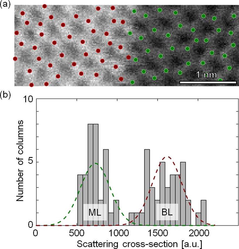
Supplemental material for:
                  Atomic-scale quantification of charge densities in 2D materials
            Knut Müller-Caspary,1, 2, 3, ∗ Martial Duchamp,3, 4 Malte Rösner,5, 6, 7 Vadim Migunov,3 Florian
              Winkler,3 Hao Yang,7 Martin Huth,8 Robert Ritz,8 Martin Simson,8 Sebastian Ihle,8 Heike
           Soltau,8 Tim Wehling,5, 6 Rafal E. Dunin-Borkowski,3 Sandra Van Aert,1 and Andreas Rosenauer2
                    1
                     EMAT, Universiteit Antwerpen, Groenenborgerlaan 171, B-2020 Antwerpen, Belgium
                           2
                             IFP, Universität Bremen, Otto-Hahn-Allee 1, 28359 Bremen, Germany
             3
               Ernst Ruska-Centre for Microscopy and Spectroscopy with Electrons and Peter Grünberg Institute,
                                      Forschungszentrum Jülich, 52425 Jülich, Germany
                      4
                        School of Materials Science and Engineering, Nanyang Technological University,
                                      50 Nanyang Avenue, Singapore 639798, Singapore
                           5
                             ITP, Universität Bremen, Otto-Hahn-Allee 1, 28359 Bremen, Germany
                          6
                            BCCMS, Universität Bremen, Am Fallturm 1, 28359 Bremen, Germany
    7
      Department of Physics and Astronomy, University of Southern California, Los Angeles, California 90089-0484, USA
                              8
                                PNDetector GmbH, Otto-Hahn-Ring 6, 81739 München, Germany

      I.    MATHEMATICAL TREATMENT OF                              The first moment of this recorded pattern is
           PARTIAL SPATIAL COHERENCE.                                                  ZZ
                                                                             h~   ~ =
                                                                              p⊥ (R)i       K(~     ~ p~⊥ d2 p~⊥ .
                                                                                               p⊥ , R)
   To derive the relations between the first moment h~
                                                     p⊥ i
                                   ~
and the projected electric field EP of the specimen in             Inserting eq. (S 2) yields
the presence of partial spatial coherence, we recall the
fully coherent result derived earlier1. By the theorem of               h~   ~ =
                                                                         p⊥ (R)i
Ehrenfest,                                                                  Z Z Z Z
                                                                                       K(~    ~ + ~s) · w(~s) d2~s p~⊥ d2 p~⊥
                                                                                         p⊥ , R
                                    Z
                       ~ =−     e        ~ ⊥ i dz
                  h~
                   p⊥ (R)i              hE
                                v                                  where it is noticed that p~⊥ can be treated constant for
                                                                   the ~s-integral. By permuting the integration sequence
where the integration is performed along the direction z           and pulling w(~s) out of the p~⊥ -integral we obtain
of the incident beam. The integral hE   ~ ⊥ i is the expec-
tation value of the electric field. For thin specimen we                h~   ~ =
                                                                         p⊥ (R)i
derived                                                                     Z Z Z Z
                                                                                     p~⊥ K(~    ~        2
                                                                                             p⊥ , R + ~s) d p~⊥ ·w(~s) d2~s .
            h~   ~ = −e E
             p⊥ (R)i                    ~
                              ~ P ∗ I0 (R)    .        (S 1)                    |              {z              }
                          v                                                                     ~ s)i
                                                                                           h~
                                                                                            p⊥ (R+~

    In the partial spatial coherent case, an extended elec-        Obviously the square brackets contain the definition of
 tron source is assumed where each point ~s gives rise to          the commonly used expectation value of the momentum
 a STEM probe at position R     ~ + ~s on the specimen. Usu-            ~ + ~s)i, however, only for a diffraction pattern that
                                                                   h~
                                                                    p⊥ (R
 ally the emitted intensity distribution w(~s) of the electron     is created by the point ~s in the emitter. Finally we get
 gun is described by a Gaussian function whose half-width          the cross-correlation (◦) integral
 at half maximum (HWHM) characterises the degree of                                      ZZ
 spatial coherence. Because all source points ~s emit in-                          ~              ~ + ~s)i · w(~s) d2~s
                                                                              h~
                                                                               p⊥ (R)i =     h~
                                                                                              p⊥ (R
 dependently from each other, a fully coherent diffraction
 pattern must be calculated for each ~s and the diffraction                                           ~
                                                                                       = (w ◦ h~
                                                                                               p⊥ i) (R)                        (S 3)
 patterns stemming from all emitters must be summed
 incoherently.                                                     telling us that the first moment of a recorded diffraction
    In the following it is assumed without loss of generality      pattern in the presence of partial spatial coherence is a
 that both w(~s) and I0 (~r − R ~ − ~s) are normalised, w(~s) ·    weighted average over all expectation values h~    ~ + ~s)i
                                                                                                                    p(R
          ~ s) being the intensity of a probe at position R+
 I0 (~r − R−~                                               ~      calculated by treating each emitter point ~s as a point-
~s. This probe gives rise to the diffracted intensity w(~s) ·      shaped, fully coherent source. Thus we can use eq. (S 1)
 K(~     ~ + ~s). The recorded diffraction pattern K(~
      p, R                                                 ~ is
                                                        p, R)      to obtain
 then the incoherent summation
                                                                                 ~ + ~s)i = − e E

                                                                                                            ~ + ~s) .
                                                                                                  ~ P ∗ I0 (R
                                                                            h~
                                                                             p⊥ (R
                     ZZ                                                                       v
        K(~     ~ =
           p⊥ , R)       K(~     ~ + ~s) · w(~s) d2~s .
                            p⊥ , R                         (S 2)   Inserting in eq. (S 3) provides eq. (1) of the manuscript.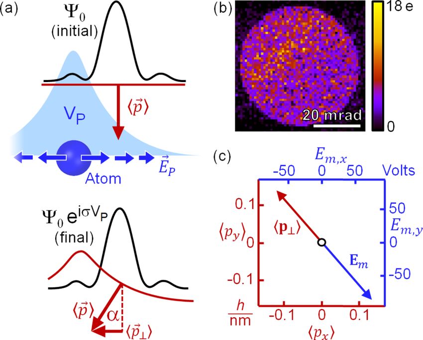
2

   Starting from Maxwell’s equation div E~ = ρ/ε0 we can
straightly calculate the measured charge density from
eq. (1) of the manuscript by considering the divergence
of both sides. Since the divergence operator in
                    nh             i    o
               div⊥    w◦ E            ~
                            ~ P ∗ I0 (R)

acts only on E ~ P , the measured charge density is the
actual projected charge density, convolved with I0 and
cross-correlated with w(s). Hence also charge densities
can be mapped quantitatively with the resolution the mi-
croscope ultimately provides.

    II.   EXPERIMENTAL AND SIMULATION
                  DETAILS

   The MoS2 sample was prepared by exfoliation2 .
An FEI Titan G2 80-200 chemiSTEM microscope at
Forschungszentrum Jülich (Germany) was operated at
80 kV with a semi-convergence angle of 24.8 mrad to
record the 4D STEM data set. The microscope is
equipped with a Schottky-type high-brightness field
emission gun (FEI X-FEG) and a CEOS DCOR corrector
for the aberrations of the probe-forming lens. Residual       FIG. S 1. Atom counting. (a) Annular dark field STEM im-
aberrations measured from a Zemlin tableau are listed         age acquired with the HAADF detector simultaneously with
in Table S 1. Diffraction patterns have been recorded on      the momentum-resolved 4D data analysed in the manuscript.
the pnCCD3,4 system operated at a speed of 4000 frames        Green and red dots mark the MoS2 mono- and bilayer.
per second in high charge handling capacity mode4 . At        (b) Distribution of scattering cross sections obtained by Gaus-
this speed the camera provides 66×264 pixels (reduced         sian modelling of the STEM image in (a). The bimodal dis-
to 662 for analysis) whereas the Ronchigram diameter of       tribution with cross sections differing by a factor of 2 proves
51 pixels assured a dense momentum space sampling at          the presence of a mono-/bilayer system.
a camera length of 165 mm.
   All multislice simulations have been performed with
the STEMsim5 software using the experimental param-           Perdew-Burke-Ernzerhof9 (PBE) functionals and a plane
eters described above and absorptive potentials6 to ac-       wave cut-off of 350 eV. All simulations were carried out
count for the attenuation of the electron beam due to         using super-cells consisting of a 1 × 16 monolayer sub-
thermal diffuse scattering. A slice thickness of 0.1 nm and   strate and a 1 × 6 monolayer on top of that (lattice con-
a small defocus of 4 nm was used as estimated from the        stant: a0 = 3.18 Å; sulfur-sulfur z-distance: 3.13 Å) us-
experiment. A specimen tilt of 7.5◦ was applied as deter-     ing 24 × 2 × 1 k-meshes. The upper layer geometry was
mined from the distortion of the MoS2 unit cell. Partial      optimized for all edge terminations until all forces were
spatial coherence was accounted for by using a Gaussian       smaller than 10−4 eVÅ−1 . We fixed the Mo z-position
effective source with a half width at half maximum of         between the flake and the substrate to 6.5 Å.
55 pm. DFT calculations were performed within the pro-
jector augmented wave (PAW) method as implemented in
                                                                   III.   STATISTICAL ATOM COUNTING.
the Vienna Ab initio Simulation Package7,8 (VASP) us-
ing the generalised gradient approximation (GGA) with
                                                                 From the ADF-STEM image in Fig. S 1 (a) we extract
                                                              the number of atoms in each projected atomic column us-
          Aberration                  Value    Angle          ing atom counting10,11 . Therefore, statistical parameter
          2-fold astigmatism (A1)     1.8 nm    -43 ◦         estimation theory is used to quantify the so-called scat-
          3-fold astigmatism (A2) 113.8 nm      -67 ◦
                                                              tering cross-sections, corresponding to the total scattered
          Axial coma (B2)             6.2 nm    156 ◦
          Spherical aberration (C3 ) -3.0 µm     n.a.         intensity for each atomic column12,13 . These scattering
          4-fold astigmatism (A3)     2.8 µm   -141 ◦         cross-sections scale with the number of atoms positioned
          Star aberration (S3)        2.2 µm    112 ◦         on top of each other. The histogram of scattering cross-
          5-fold astigmatism (A4) 120.7 µm      -45 ◦         sections is shown in Fig. S 1 (b) for all atomic columns
                                                              depicted in (a). Due to the partial coherence and lim-
TABLE S 1. Measured residual aberrations of the probe cor-    ited stability of the microscope operated at low voltage
rector.                                                       (80 kV), the Mo and the S2 columns are not distinguish-
3
able here, so that a possible fine structure within each of electric field maps and is responsible for the apparently
the histogram peaks is not resolved. On the basis of a more complex electric field distribution. The fully coher-
quantitative analysis of the scattering cross-sections, we ent result in Fig. S 3 (a) shows the expected replication of
conclude the presence of atomic columns having either 1 the legend’s colorwheel.
or 2 molybdenum atoms/sulfur dimers projected on top
of each other. These results are indicated in Fig. S 1 (a) as
green and red dots corresponding to a mono- and bilayer, C. Phase approximation
respectively. This statistical analysis clearly confirms the
presence of a mono- and a bilayer in the sample. As stated by eq. (1) of the manuscript, the measured
electric field is a convolution of the actual electric field
projection with the intensity of the incident probe, fol-
IV. SIMULATION STUDIES OF FOCUS lowed by a cross correlation with the function w(~s) de-
DEPENDENCE, SPATIAL COHERENCE AND scribing the source size broadening for thin specimen.
VALIDITY OF THE PHASE APPROXIMATION We hence show that, in addition to the dynamic mul-
tislice simulations used throughout the manuscript, the
A. Focus dependence phase approximation yields identical results. Fig. S 3 (c-
e) depicts the three individual steps of this operation
On a practical concern, the probe focus is the ex- for the MoS2 monolayer, i.e. the projected electric field
perimental parameter determining Ψ0 most, and hence E~ P (figure part c), its convolution with the probe inten-
the intensity distribution of the incident STEM probe sity I0 as calculated from the experimental conditions in
I0 = Ψ0 Ψ̄0 . The focus is adjusted steadily with a preci- Tab. S 1 (figure part d), and subsequently the cross cor-
sion of a few nm in experiment. Figure S 2 shows an eval- relation with the source size broadening (figure part e).
uation of the charge density in an MoS2 monolayer from Since Figs. S 3 (a) and (d) agree quantitatively, as well as
simulated 4D STEM data using multislice. The simula- Figs. S 3 (e) and Fig. 3 (b) of the manuscript (first row),
tion includes partial spatial coherence with a source size the results can be interpreted in terms of the phase ap-
broadening according to a Gaussian with a half width at proximation.
half maximum (HWHM) of 55 pm. The probe focus was
varied between −20 nm and +18 nm, showing that the fo-
cal range of ±6 nm for succesful mapping is very narrow.
Most importantly there is no dependence of the obtained
pattern, hence slightly defocusing the probe only involves
an overall damping of the result. For the simulations in
Figs. 3 and 4 of the manuscript a defocus of 4 nm was
used. Note that focus can vary also throughout a single
image, or change slightly between the time of focusing
and the recording due to specimen and instrument insta-
bility.
B. Spatial coherence effects
Given the coherent STEM probe diameter of the micro-
scope, one would expect the electric field at atomic sites
to show up as copies of the colorwheel used as legend,
e.g., in Fig. 2 (a) of the manuscript. However, as derived
above, the recorded diffraction pattern is an incoherent
summation over all diffraction patterns arising from dif-
ferent points of emission in the electron gun, weighted by
their respective intensities, see eq. (S 2). All multislice
results in the manuscript (Figs. 3, 4) have been obtained
in this manner. It is nevertheless instructive to study
the actual impact of the incoherent summation on the
measured electric field and charge density, so that the
fully coherent multislice result is presented in Fig. S 3 (a)
and (b), respectively. By comparison with their partially
coherent counterparts in Fig. 3 (b,c) (first row) of the
manuscript it is seen that indeed the finite spatial coher-
ence of the electron source limits the resolution of the4
FIG. S 2. Simulated focus dependence of charge density maps in ML MoS2 . Diffraction patterns have been simulated with the
STEM probe foci indicated, including partial spatial coherence. The first moment of all diffraction patterns was calculated,
~ m according to eq. (1) of the manuscript. Taking the divergence and
yielding the simulated measurement of the electric field E
multiplying with ε0 as stated by eq. (2) results in the data shown. The experimental specimen tilt as mentioned above was
accounted for.
FIG. S 3. Effect of diffraction-limited probe size and partial spatial coherence demonstrated at an MoS2 ML. (a) Fully coherent
multislice simulation of the experimental 4D STEM data set and evaluation of the electric field. Except for the partial spatial
coherence, it is fully analogous to the simulation in Fig. 3 (b) (first row). (b) Charge density determined from the simulation
~ P of the ML. (d) Electric field from (c) convolved with the intensity I0 of the STEM probe.
in (a). (c) Projected electric field E
(e) Electric field from (d) cross-correlated with the emission function of the field emission gun equal to a Gaussian with a
HWHM of 55 pm, according to E ~ m in eq. (1) of the manuscript. Note that (a) is the multislice result while the equivalent
result in (d) relies on the phase approximation. Furthermore, the actual specimen tilt was used to calculate E ~ P , so that the
two sulfur atoms appear slightly separated in (c).5
∗
Corresponding author; k.mueller-caspary@fz-juelich.de Midgley (Springer, 2007) pp. 169–172.
1 6
K. Müller, F. F. Krause, A. Beche, M. Schowal- A. Weickenmeier and H. Kohl, Acta Crystallogr., Sect. A
ter, V. Galioit, S. Löffler, J. Verbeeck, J. Zweck, 47, 590 (1991).
7
P. Schattschneider, and A. Rosenauer, Nature Commu- G. Kresse and J. Hafner, Phys. Rev. B 47, 558 (1993).
8
nications 5, 5653:1 (2014). G. Kresse and J. Furthmüller, Computational Materials
2
F. Winkler, A. H. Tavabi, J. Barthel, M. Duchamp, Science 6, 15 (1996).
9
E. Yucelen, S. Borghardt, B. E. Kardynal, and R. E. J. P. Perdew, K. Burke, and M. Ernzerhof, Phys. Rev.
Dunin-Borkowski, Ultramicroscopy in press, 1 (2016). Lett. 77, 3865 (1996).
3 10
K. Müller, H. Ryll, I. Ordavo, S. Ihle, L. Strüder, K. Volz, S. Van Aert, K. J. Batenburg, M. D. Rossell, R. Erni, and
J. Zweck, H. Soltau, and A. Rosenauer, Appl. Phys. Lett. G. Van Tendeloo, Nature 470, 374 (2011).
11
101, 212110 (2012). S. Van Aert, A. De Backer, G. T. Martinez, B. Goris,
4
H. Ryll, M. Simson, R. Hartmann, P. Holl, M. Huth, S. Bals, G. Van Tendeloo, and A. Rosenauer, Phys. Rev.
S. Ihle, Y. Kondo, P. Kotula, A. Liebel, K. Müller-Caspary, B 87, 064107 (2013).
12
A. Rosenauer, R. Sagawa, J. Schmidt, H. Soltau, and S. V. Aert, J. Verbeeck, R. Erni, S. Bals, M. Luysberg,
L. Strüder, Journal of Instrumentation 11, P04006 (2016). D. V. Dyck, and G. V. Tendeloo, Ultramicroscopy 109,
5
A. Rosenauer and M. Schowalter, in Springer Proceedings 1236 (2009).
13
in Physics, Vol. 120, edited by A. G. Cullis and P. A. A. D. Backer, K. van den Bos, W. V. den Broek, J. Sijbers,
and S. V. Aert, Ultramicroscopy 171, 104 (2016).You can also read