Comparative Analysis of Ultra-Low Current Measurement Topologies With Implementation in 130 nm Technology
←
→
Page content transcription
If your browser does not render page correctly, please read the page content below
Received March 1, 2021, accepted April 10, 2021, date of publication April 20, 2021, date of current version May 3, 2021.
Digital Object Identifier 10.1109/ACCESS.2021.3074464

Comparative Analysis of Ultra-Low Current
Measurement Topologies With Implementation
in 130 nm Technology
SARATH KUNDUMATTATHIL MOHANAN 1,2 , HAMZA BOUKABACHE                                                                1,   (Member, IEEE),
DANIEL PERRIN 1 , AND ULLRICH R. PFEIFFER 2 , (Fellow, IEEE)
1 HSE-RP-IL,   CERN, 1211 Geneva, Switzerland
2 IHCT,   University of Wuppertal, 42119 Wuppertal, Germany
Corresponding author: Sarath Kundumattathil Mohanan (sarath.mohanan@cern.ch)

  ABSTRACT Radiation detectors need front-end electronics capable of measuring currents over a large
  dynamic range with femtoampere sensitivity. The goal of this work is to find an alternative to the legacy
  systems implemented using discrete components or technology nodes of 350 nm or higher. The 130 nm
  technology is evaluated on its leakage current performance to assess its employability in such applications.
  A comparative analysis of three low current measurement topologies, namely the charge balancing, reset
  counting, and direct slope measurement methods, is carried out and their performance in different current
  ranges is evaluated. The charge balancing method was found to provide a better dynamic range with greater
  accuracy. However, in the lower current range, the direct slope measurement method was found to give
  faster results than the other two methods with comparable accuracy. Also, an application-specific integrated
  circuit implementing the charge balancing method was found to be linear throughout the dynamic range of
  −1 fA to −1 µA and could measure currents with an accuracy of ±7%. This achievement in the 130 nm
  technology opens the way to using the high-speed digital cells offered by this technology in conjunction with
  the low-leakage transistors to design a high-speed accurate current measurement system.

  INDEX TERMS Femtoampere measurement, radiation detector, low current measurement.

I. INTRODUCTION                                                                                 and the gate oxide thickness will negatively affect the leakage
Femtoampere current measurements face numerous chal-                                            currents [5], rendering the advanced nodes unusable for low
lenges owing to the very minuscule nature of the signal that                                    current measurements. It is unfortunate that the numerous
needs to be sieved out from the vast sea of noise sources.                                      processing capabilities often required in making fast com-
In most current measurement applications, currents below                                        putations for real-time current monitoring systems appear
picoamperes are considered to be leakage currents [1], [2].                                     elusive for these applications because of the high leakage
However, for specific applications, such as biomedical signal                                   current. A solution in this scenario is to use a two-chip
processing [3] and environmental radiation monitoring [4],                                      system that has the leakage-critical analog part in a higher
accurate measurements in the femtoampere range are often                                        technology node and the high-speed digital section in a
required. The bottleneck in such applications is elimination                                    lower technology node or a modern field-programmable gate
of the intrinsic leakage currents associated with the technol-                                  array (FPGA). To avoid the complexities associated with
ogy being used and the measurement environment. These                                           a two-chip solution and to bring the overall cost down,
leakage currents depend on many factors and are not easily                                      a technique of using the IO transistors for the entire analog
compensated for by calibration. To attain the goal of fem-                                      section and core transistors for the digital section is proposed
toampere sensitivity, it is important to choose a technology                                    here.
for which the intrinsic leakages are in this range or lower.                                       A femtoampere-sensitive current digitizer was designed
As the technologies scale down, shrinking the channel length                                    at European Organization for Nuclear Research (CERN),
                                                                                                in AMS 350 nm technology [6]. The leakage current of
   The associate editor coordinating the review of this manuscript and                          this technology node is low enough to attain the required
approving it for publication was Cihun-Siyong Gong               .                              sensitivity. Much work has been done in the technology

                      This work is licensed under a Creative Commons Attribution 4.0 License. For more information, see https://creativecommons.org/licenses/by/4.0/
VOLUME 9, 2021                                                                                                                                                         63855
S. K. Mohanan et al.: Comparative Analysis of Ultra-Low Current Measurement Topologies

node of 350 nm or higher for ultra-low current measure-
ments [2], [7]–[10]. An implementation in 180 nm technol-
ogy [11] reports a current resolution of 314 fA, and another
in 130 nm [12] attains a sensitivity of 135 fA. However,
no work has been reported in 130 nm or lower that mea-
sures current with 1 fA sensitivity and with a dynamic range
extending up to microamperes. Therefore, for low current
measurement applications, as an alternative to the popular
350 nm node, TSMC 130 nm technology is evaluated in this
study. The core transistors were found in simulations to have
leakage currents on the order of picoamperes and are not the
most suitable candidates for this application. The IO transis-
tors operating with a supply voltage of 3.3 V have thick gate
oxides and leakage currents in the femtoampere range. This           FIGURE 2. Current-to-frequency converter output.

work aims to characterize the leakage currents associated
with the IO transistors of the TSMC 130 nm technology and
                                                                     then resets the feedback capacitor of the CFC. An external
to evaluate the employability of this technology in low current
                                                                     circuit counts the number of pulses.
applications. In the course of designing current measurement
                                                                        The output of the circuit in Fig. 1 is shown in Fig. 2. The
circuits, three basic circuit topologies were evaluated to dif-
                                                                     number of pulses in a fixed amount of time is proportional to
ferentiate their capabilities. The limitations associated with
                                                                     the input current. The measured current Iin is given by
each approach and the performance over different current
ranges are extensively studied and demonstrated.                                               NCf (Vth − Vcm )
                                                                                           Iin =                ,                (1)
                                                                                                      T
II. LOW CURRENT MEASUREMENT TOPOLOGIES                               where N is the number of resets in the measurement time T ,
Current-to-frequency conversion (CFC) is the most com-               Cf is the feedback capacitor, Vcm is the initial voltage at the
monly used technique to measure very low currents [13], [14].        output of the integrator and equals the common mode voltage
A CFC circuit consists of an operational transconductance            of the OTA, and Vth is the threshold voltage of the comparator.
amplifier (OTA) with a feedback capacitor and a reset
switch. The current to be measured charges the capacitor and         B. DIRECT SLOPE MEASUREMENT
thereby produces an output with a slope of integration propor-       In this method, the output of the CFC is fed to two com-
tional to the input current. Measurement of this slope enables       parators with different threshold voltages, as shown in Fig. 3.
one to calculate the input current. The slope measurement can        The measurement of the time difference between the two
be accomplished in multiple ways. Three basic approaches             threshold crossings enables calculation of the slope of the
are explained in the following.                                      CFC output, which is proportional to the input current.

FIGURE 1. Reset counting method.
                                                                     FIGURE 3. Direct slope measurement.

                                                                        The input current can be calculated from
A. RESET COUNTING METHOD
                                                                                               Cf (Vth2 − Vth1 )
The circuitry for this method [15] is shown in Fig. 1.                                     Iin =                 ,                (2)
A comparator produces an output each time the CFC output                                            t2 − t1
crosses a threshold. When the comparator output is high,             where Vth2 and Vth1 are the threshold voltages of the compara-
a pulse generator produces a pulse of fixed length. This pulse       tors, with Vth2 > Vth1 , and t2 and t1 are the respective times

63856                                                                                                                            VOLUME 9, 2021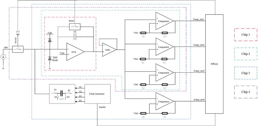
S. K. Mohanan et al.: Comparative Analysis of Ultra-Low Current Measurement Topologies

                                                                                FIGURE 5. Transistor characteristics for TSMC 130 nm and AMS 350 nm
                                                                                NMOS transistors with W /L = 1 µm/1 µm, Vds = 0.1 V.
FIGURE 4. Charge balancing method.

of arrival of the falling edges of the comparator outputs Vout2
and Vout1 in the measurement system. The output Vout2 may
be used to generate the reset pulse for the feedback capacitor
to start the next measurement cycle.

C. CHARGE BALANCING METHOD
In the charge balancing method [16], shown in Fig. 4,
a reference charge is added to or subtracted from the feedback
capacitor each time the CFC output crosses the threshold.
The number of charge injections is proportional to the input
current and can thus be calculated. The input current in this
topology is calculated as                                                       FIGURE 6. Transistor characteristics for TSMC 130 nm and AMS 350 nm
                                                                                PMOS transistors with W /L = 1 µm/1 µm, Vds = 0.1 V.
                                    NQref
                            Iin =         ,                           (3)
                                     T
where Qref is the reference charge generated by the charge                      was 178 pA, and that of the corresponding IO transistor was
pump, N is the number of charge injections, and T is the                        460 fA. The analogous characteristics for PMOS transistors
measurement time interval.                                                      are shown in Fig. 6.
   Besides the three methods described above, other tech-                          The off currents associated with the PMOS transistors were
niques, such as ADC sampling of the integrator slope or use                     simulated to be 22 aA for the AMS core transistor, 33 fA for
of a transimpedance amplifier for current conversion, are                       the TSMC IO transistor, and 74 pA for the TSMC core tran-
available [1], [11], [12], [17], [18], but these methods                        sistor. The core transistors of the TSMC 130 nm node showed
are not considered in the present study. Other novel solu-                      leakages on the order of picoamperes and hence could not
tions for ultra-low current measurement employ technolo-                        be directly used in femtoampere measuring systems. As an
gies such as single-electron pumps or ultra-low noise current                   alternative to AMS 350 nm transistors, the IO transistors of
amplifiers [19].                                                                the TSMC 130 nm node looked promising in terms of offering
                                                                                comparable leakage performance. Another main candidate
III. TECHNOLOGY EVALUATION                                                      was the gate leakage current, which at lower technologies
The technology of interest, the TSMC 130 nm node, was                           such as 130 nm could be significant for low current appli-
evaluated in terms of the leakage currents. A comparison of                     cations. However, the unavailability of accurate gate leakage
the drain-to-source current variation with the gate-to-source                   models for simulation make estimation of this leakage current
voltage for the NMOS transistors of the AMS 350 nm and                          difficult, necessitating the use of test structures to quantify it.
TSMC 130 nm technologies is shown in Fig. 5. The spectre                        With the thick gate IO transistors rated for 3.3 V, their leakage
simulations were carried out by varying the gate voltage and                    current was expected to be comparable to that of the core
tying the source and bulk terminals to the ground. The drain                    AMS 350 nm transistors.
terminal was held at a voltage of 0.1 V, which was found to be
the maximum voltage that could appear across the drain and                      IV. SYSTEM DESIGN
source terminals (Vds) of the switches in their off state in the                To evaluate different topologies, four test chips were designed
circuit implementations considered here.                                        in TSMC 130 nm technology. Chip 1 is made of two channels,
   The off current observed for the AMS 350 nm NMOS core                        with the first channel having electrostatic discharge (ESD)
transistor was 40 fA, that of the TSMC 130 nm core transistor                   diodes in its input path and the second one without any

VOLUME 9, 2021                                                                                                                                 63857
S. K. Mohanan et al.: Comparative Analysis of Ultra-Low Current Measurement Topologies

FIGURE 7. System architecture.

ESD structures. The two channels are identical and each                 integrator. The folded cascode OTA topology of the
consists of an integrating amplifier with a reset switch. The           UTOPIA 2 application-specific integrated circuit (ASIC) [21]
purpose of the chip is to determine whether the integrator can          designed in AMS 350 nm was adopted for the integrator
distinguish currents with femtoampere sensitivity by integrat-          realization. The input stage of the OTA was realized using
ing them with various slopes.                                           PMOS transistors because of their intrinsic low-noise behav-
   Given that ESD diodes have been identified as the main               ior and lower leakage compared with the NMOS transistors,
sources of leakage in femtoampere measurements [20],                    as observed from the simulations.
the chip also aims to identify the leakage currents associated             A voltage follower isolates the OTA section from the
with the ESD diodes in this technology.                                 comparators. To minimize the effect of noise on comparator
   Chip 2 also has two channels, which, in addition to the              switching, resistors R1 and R2 are used to provide hysteresis.
integrator in Chip 1, have three comparators with different             The threshold points of switching are calculated as
threshold voltages for performing current measurement with
the direct slope or reset counting method. The second channel                                                        R2
                                                                                      UTP = Vth + (Vsatp − Vth )          ,                    (4)
has floating input and its purpose is to identify all the leakages                                                R1 + R2
in the system.                                                                                                       R2
                                                                                       LTP = Vth + (Vsatn − Vth )         ,                    (5)
   Chip 3 incorporates the charge balancing method and has                                                        R1 + R2
dedicated blocks for charge generation using switched capac-
itors and a clock generator to generate the clocks for the              where UTP is the upper threshold point, LTP is the lower
switched capacitor.                                                     threshold point, Vsatp is the positive saturation voltage of
   Chip 4 is similar to Chip 2 but has an additional switch in          the comparator, Vsatn is the negative saturation voltage, Vth
the input path. This switch is closed during the integrating            is the threshold voltage, and R1 and R2 are the feedback
phase and opens when the integrator is in reset. This helps to          resistors. Values of 20 k and 3 k were used for R1 and R2 ,
eliminate the charge loss during the reset period. Chip 4 aids          respectively. The threshold voltages for the comparators were
in understanding the effects of inclusion of such a switch in           generated externally using programmable precision digital-
the input path.                                                         to-analog convertors (DACs).
   The system architecture, with details of the four chips,                For direct slope measurement, three sets of values can
is displayed in Fig. 7. For Chips 1, 2, and 4 the depicted              be calculated by measuring the time difference between the
section shows the first channel. These chips also have an               falling edges of the three comparators. The output from
identical second channel for leakage current measurement.               the third comparator is used to generate the reset signal.
At the heart of all the topologies is an integrator. An oper-           The charge balancing method has a charge generation block
ational amplifier or OTA may be used to realize the                     where a switched capacitor Cref is charged to a reference

63858                                                                                                                               VOLUME 9, 2021
S. K. Mohanan et al.: Comparative Analysis of Ultra-Low Current Measurement Topologies
voltage Vref , thereby generating a charge
Qref = Cref Vref . (6)
The reference charge is then subtracted from the charge stored
in the feedback capacitor. The reference charge generation
and subsequent discharge are controlled by the switches
S1–S4 of the switched capacitor. S3 and S4 are used to
remove any residual charge in Cref . S2 connects Cref to Vref ,
and later S1 connects Cref to the input path. The generation of
the control signals is carried out by the clock generator block
according to the enable signal, which is a pulse generated FIGURE 8. Percentage error in current measurement versus the reset
based on the output of the fourth comparator. An FPGA duration for an input current of 10 µA with and without correction.
is responsible for generating the reset and enable signals
and receiving the comparator outputs to perform the current
calculation. can be minimized. The reset time does not have any effect
on the threshold crossing method and the charge balancing
V. EFFECT OF NONIDEALITIES ON method, since this time does not come into play in the regular
CURRENT MEASUREMENT measurement interval.
Current calculation in all three methods using (1)–(3)
assumes ideal components and conditions. However, there B. COMPARATOR DELAY
are many factors that can affect each term in the current The rise and fall times of the comparator directly mani-
calculation and lead to erroneous results. fest as its propagation delay. This delay of the comparator
also affects the current measurement in the reset counting
A. RESET DURATION method. The comparator delay in turn appears as a shift in
In the reset counting method, the capacitor terminals are the threshold voltage, and the integrator output overshoots
shorted through a reset switch each time the integrator output the threshold. If this delay could be accurately determined,
reaches a threshold voltage. The time t required to reset the it could be compensated for in the same way as in (8), with
integrator by discharging the capacitor Cf is proportional to Trst replaced by Tc , the delay associated with the comparator.
the on resistance of the transistor switch, Ron : The delay should be limited so that the integrator output does
Vinit
not reach saturation. In the direct slope method, the match-
t = Ron Cf ln . (7) ing between two comparator delays affects the accuracy.
Vt
Since the threshold voltages of the comparators are different,
In (7), Vinit is the initial voltage across the capacitor and Vt the associated propagation delays also differ. The comparator
is the final voltage. A transistor with W /L = 4 µm/350 nm delay thus acts as the main source of error in this method for
was simulated to have an on resistance of 600 . There are currents of tens of nanoamperes and above. The comparator
two transistors in series in the reset path, making an on resis- delay has almost no impact on measurement in the charge bal-
tance of 1.2 k for the switch. The time to discharge a 1 pF ancing method, since the quantum of charge being subtracted
capacitor completely through this resistance is around 6 ns. is determined by a separate charge generation circuit that is
This reset time results in fewer resets in the measurement time independent of the comparator parameters.
Tm compared to the ideal case. The current calculation in (1)
can be modified to include the reset time Trst : C. COMPARATOR THRESHOLD
NCf (Vth − Vcm ) The comparator threshold affects the charge that is built up
Iin = . (8) in the feedback capacitor in each reset cycle. In the reset
T − NTrst
counting method, the comparator threshold is proportional
The correction factor helps to minimize the error. A plot of the to the gain of conversion, so the current calculation gets
error in current measurement for an input current of 10 µA modified to
with and without correction for a range of reset times is shown
NCf (Vth − Vcm + 1Vth )
in Fig. 8. Iin = , (9)
The measurement time T was chosen as 100 ms, Cf was T
set to 1 pF, and 1V was taken to be 0.5 V. From the graph it where 1Vth is the change in the threshold voltage. The direct
is clear that the effect of the reset time can be compensated slope method is heavily dependent on the matching between
for with minimal impact on accuracy. The residual error is the threshold voltages of the comparators. By using more
mainly due to the quantization effect arising from the fact than two comparators, a better estimate of the slope can be
that N is an integer. The correction works when the total obtained and the deviation in the threshold voltages can be
measurement time T
Trst . Thus, the effect of the reset averaged out. From (3), the comparator parameters do not
time on measurement accuracy in the reset counting method affect the conversion gain in the charge balancing method,
VOLUME 9, 2021 63859S. K. Mohanan et al.: Comparative Analysis of Ultra-Low Current Measurement Topologies
and hence this method is immune to changes in the threshold Different sources of leakage for a current measurement
voltages of the comparators. ASIC have been studied and characterized for the AMS
350 nm technology in [22]. The sources of leakages from the
D. OTA OFFSET circuit point of view are the drain-to-source leakage of the
The finite input offset voltage of the OTA affects the cal- reset switch, the gate leakage current of the input transistors,
culation in the reset counting method in the same way as and the leakage current of the ESD diodes. The charge bal-
the comparator threshold voltage. This is because, instead of ancing method has additional switches for charge injection,
starting the integration from Vcm , it starts from Vcm + Vos : which contribute extra leakage currents. Chip 4 with the input
series switch also has also an additional leakage current.
NCf (Vth − Vcm − Vos ) Consider a system with a leakage current Ileak . Let 1V
Iin = , (10)
T be the difference between the initial voltage of the integrator
where Vos is the offset voltage of the OTA. The OTA offset output and the threshold voltage, and let Cf be the feedback
does not have any effect on the direct slope method since it capacitor. To distinguish a signal of magnitude Imin , the min-
gets cancelled out in the calculation. The charge generation in imum measurable current, the minimum time resolution 1t
the charge balancing method depends on the voltage to which that must be measured with precision is
the switched capacitor is connected. Thus (3) gets modified to Cf · 1V · Imin
1t = , (13)
NCref (Vref − Vos ) Ileak (Ileak + Imin )
Iin = . (11)
T or
E. RESISTOR VALUES Cf · 1V · Imin
1t ∼
= 2
. (14)
The accuracy of the feedback resistors determines the thresh- Ileak
old voltage, and a change in the resistor values by process The challenge is accurately measuring this time difference.
variation affects the current calculation in the same way as a For a system with a leakage of 1 pA, assuming Cf to be
change in comparator threshold. For the direct slope method, 1 pF and 1V to be 0.1 V, the 1t required to measure 1 aA is
the effective voltage difference in threshold voltages is 100 ns, which is theoretically possible. However, the leakage
R1 current does not remain constant and is heavily dependent on
1V = (Vth2 − Vth1 ) . (12) temperature, voltage, and process variations. This variation
R1 + R2
makes it even more challenging to calibrate out the leakage
The accuracy of the resistors therefore affects the accuracy current. Even though, theoretically, measurement down to
of measurement. By measuring the UTPs using (4) for the attoamperes is possible with all the measurement topologies,
two different threshold voltages, the resistor values can be 1 fA is a reasonably observed limit in standard laboratory
calibrated. In the charge balancing method, like the other conditions.
comparator parameters, resistor values have minimal impact.
B. UPPER LIMIT
F. CAPACITOR VALUES There are many circuit elements limiting the maximum cur-
The values of the feedback and charge balancing capacitors rent that can be measured by the different topologies. The
can affect the measurement and need to be calibrated. nonidealities described in Section V are the major factors
that limit the maximum current measurable with the required
G. SWITCHED CAPACITOR NONIDEALITIES accuracy. Calibration helps to minimize the nonidealities to
Effects such as charge injection and clock feed-through can a certain extent, beyond which the error in measurement
have an impact on the charge generation and discharge in the increases. Apart from the aforementioned factors, the main
charge balancing method. Proper sizing of the switches of limiting factor in the measurement is the OTA.
the switched capacitor and accurate timing of the clocks can The OTA remains stable until an input measured current is
reduce these effects [21]. comparable to the bias current that flows through the output
stage of the OTA. In the present design, this bias current is
VI. CURRENT MEASUREMENT LIMITS around 140 µA. For input currents above the bias current,
A. LOWER LIMIT the operating point of the OTA shifts, which results in the
The lowest measurable current is strictly a limitation imposed output shifting from the common mode voltage. The OTA
by numerous factors, the most prominent among them being loses its linearity in this region of operation.
the leakage current in the system itself. It is a cumulative The sizing of the transistors forming the reset switch is
contribution linked to the technology, the circuit topology, another factor that can result in a shift of the OTA output
and the measurement setup. The accuracy of the current from the initial value. For higher currents, the drain terminal
generating source and the means by which it is transported of the transistor that is connected to the OTA output moves
to the measurement circuitry also limits the magnitude of the to increase the drain-to-source voltage. This in turn shifts
minimum current that can be accurately measured. the output voltage. When a minimum-sized transistor is used
63860 VOLUME 9, 2021S. K. Mohanan et al.: Comparative Analysis of Ultra-Low Current Measurement Topologies
as the reset switch, as the input current is increased from that generates the reference charge:
1 µA to 10 µA, the initial output voltage of the OTA shifts
Vref
by 300 mV, which reduces the effective voltage headroom Imax = , (16)
for slope measurement before the OTA output saturates. 5(Ron1 + Ron2 )
This issue can be minimized by increasing the width of the where Ron1 and Ron2 are the on resistances corresponding
transistor switch, thereby increasing the drain current for to the transistor switches that connect the capacitor to the
smaller drain-to-source voltage. The transistor sizing is thus reference voltage and the OTA input, respectively. For a
a tradeoff between the leakage current and the maximum reference voltage of 1 V and simulated on resistances, Imax is
current to be measured. A T-switch having three transistors calculated as 2.6 µA.
with W /L = 4 µm/350 nm can attain the required leakage
below femtoampere level and support the maximum current VII. MEASUREMENT SETUP
until the limitation of 140 µA of the OTA is reached. The test chips were directly wire-bonded onto an FR4 printed
Each topology has dedicated additional circuitry that fur- circuit board as shown in Fig. 9. Packaging was avoided to
ther imposes limits on the maximum measurable current. eliminate unwarranted leakage from the package. The test
board generates the power supplies and houses the DACs
1) RESET COUNTING METHOD to generate precise bias and threshold voltages for the chip.
Considering the effects of all the nonidealities, the current An FPGA board receives the comparator outputs of the chip,
calculation can be modified to generates the control signals, and programs the DACs.
N α Cf (Vth − Vcm − Vos − 1Vth )
Iin = , (15)
T − NTrst − βNTc − Td
where α is the correction factor from the calibration of the
capacitor value, Tc is the comparator delay, Td is the delay
due to the digital logic in the FPGA that generates the reset
signal, 1Vth is the mismatch in the comparator threshold, and
β is the proportionality factor for the delay associated with the
comparator and takes into account its dependency on the input
current; hence this factor was formulated as a ratio with the
reset count N which is the best estimate of the input current.
Most of the nonidealities identified in (15) are constants
and can be corrected by calibration. The main limiting factors
are the comparator delay and finding a constant value for β
for a wide range of input currents. This limits the maximum
current that can be accurately measured with this method.
Consider a 3.3 V system with a 1 pF feedback capacitor. FIGURE 9. Bonded chip.
Assuming a total delay of 50 ns for the comparator and digital
section, for an input current of 15 µA and above the OTA The current was injected from a Keithley 6430 current
output approaches saturation and loses linearity. source. The outputs captured from the chip on an oscilloscope
Increasing the feedback capacitor makes the system slower were transferred to a computer through Ethernet. The current
and reduces the impact of the comparator delay on the mea- calculations were carried out in the FPGA. The whole data
surement for higher currents. Thus there is a tradeoff between capture was controlled from a MATLAB environment inter-
the frequency of operation of the CFC and the desired upper faced to the FPGA board through an universal asynchronous
current limit. receiver-transmitter. The experiment was carried out under
standard laboratory conditions, and the chip was shielded in
2) DIRECT SLOPE METHOD a metallic enclosure for protection against perturbations for
The limitation in this method arises from the precise mea- Electromagnetic Compatibility.
surement of the time between two comparator outputs. For a
system in the above example with an input current of 5 µA VIII. MEASUREMENT RESULTS
and a threshold voltage difference of 0.1 V, the time to mea- The current generated by the ionization chambers, which
sure is 20 ns. Given the nonconstant delay associated with the is the target application, is typically negative. The slope
comparator, measurement in this range is greatly error prone. of the integrator output is positive for negative current and
vice versa.
3) CHARGE BALANCING METHOD The output of the OTA obtained from the first channel of
The maximum measurable current in this method is deter- Chip 1 is shown in Fig. 10. The measurement was carried
mined by the charging and discharging time of the capacitor out in a controlled environment at 25◦ C. The slope of the
VOLUME 9, 2021 63861S. K. Mohanan et al.: Comparative Analysis of Ultra-Low Current Measurement Topologies
FIGURE 10. OTA output of Chip 1 with input current swept from 7.5 fA
to −7.5 fA.
FIGURE 11. The measured current and corresponding percentage error
output is close to zero for an input current of 7.5 fA. This with input current swept from −1 fA to −25 fA with the reset counting
represents the cumulative leakage currents at the input. Apart method.
from the leakages associated with the printed circuit board
and the cable, the leakage of the ESD diodes, the gate leakage
of the input transistors of the OTA, and the leakage current
of the transistor in the reset switch are all included in this
input bias current. From Fig. 10 it can be seen that the chip
distinguishes current with 1 fA sensitivity. A common mode
voltage of 2.2 V was chosen for the OTA and so it integrates
from this value.
The second channel, without the ESD diodes, produced a
similar response but the bias current was found to be 2 fA.
A total of five chips were evaluated for leakage currents and
the results are summarized in Table 1.
TABLE 1. Measured input leakage currents.
FIGURE 12. The measured current and corresponding percentage error
with input current swept from −1 fA to −1 µA with the charge balancing
method.
All the chips with ESD diodes in the input reported leakage the methods exhibited similar behavior, only the result of the
currents of 7 fA. The second channel in Chip 1 had no ESD reset counting method, which had the highest maximum error
diodes and hence reported a leakage current of only 2 fA. (−9.4%), is shown here. The maximum error reported by the
The additional input switch of Chip 4 added 3 fA to the charge balancing method in the −1 fA to −25 fA band was
leakage. Similarly, the three switches for charge injection in −7.2 %. Of the three methods, direct slope measurement was
Chip 3 contributed an additional 3 fA, making a total leakage found to have the smallest errors, with the maximum error
current of 10 fA. reported as −7%.
A. MEASUREMENT RESULTS IN THE B. MEASUREMENT RESULTS IN THE FEMTOAMPERE
FEMTOAMPERE RANGE TO MICROAMPERE RANGE
All three methods produced linear results when injected with As the input current was increased, the charge balancing
an input current ranging from −1 fA to −25 fA. The results method was found to perform better than the other two meth-
from the reset counting method are displayed in Fig. 11. The ods. Fig. 12 shows the linearity and error plot for currents of
current values shown are absolute values without taking the up to −1 µA for the charge balancing method. The output of
polarity into consideration. the chip was found to be linear over the entire measurement
The input leakage current was measured and compensated range, and the percentage error in the considered dataset
for while plotting the graph for better visualization. Since all remained within ±3%. The leakage current was compensated
63862 VOLUME 9, 2021S. K. Mohanan et al.: Comparative Analysis of Ultra-Low Current Measurement Topologies
for in post-processing for this plot as well. With the other two [3] A. Gore, S. Chakrabartty, S. Pal, and E. Alocilja, ‘‘A multi-channel
methods, for an input current above −10 nA, the comparator femtoampere-sensitivity conductometric array for biosensing applica-
tions,’’ in Proc. IEEE Eng. Med. Biol. Soc. Int. Conf., Aug. 2006,
delay resulting in the threshold shift and the subsequent pp. 6489–6492, doi: 10.1109/IEMBS.2006.260865.
overshoot of the integrator output before it was reset led to [4] H. Boukabache, M. Pangallo, G. Ducos, N. Cardines, A. Bellotta, C. Toner,
errors above 10%. D. Perrin, and D. Forkel-Wirth, ‘‘Towards a novel modular architecture
for CERN radiation monitoring,’’ Radiat. Protection Dosimetry, vol. 173,
nos. 1–3, pp. 240–244, Apr. 2017, doi: 10.1093/rpd/ncw308.
IX. DISCUSSION [5] P. M. Zeitzoff and H. R. Huff, ‘‘MOSFET scaling trends, challenges, and
key associated metrology issues through the end of the roadmap,’’ AIP
A detailed comparison of different low current measurement Conf. Proc., vol. 788, pp. 203–213, Sep. 2005, doi: 10.1063/1.2062964.
topologies has revealed the vulnerabilities and advantages [6] E. Voulgari, M. Noy, F. Anghinolfi, F. Krummenacher, and M. Kayal,
associated with each of them. It was found that the three meth- ‘‘Design and measurement methodology for a sub-picoampere cur-
ods performed equally well in the femtoampere measurement rent digitiser,’’ in Proc. 22nd Int. Conf. Mixed Design Integr. Circuits
Syst. (MIXDES), Jun. 2015, pp. 525–529, doi: 10.1109/MIXDES.2015.
range. The charge balancing method was found to have the 7208578.
highest dynamic range and better immunity to nonidealities. [7] M. Zhang, N. Llaser, and H. Mathias, ‘‘A low noise CMOS preamplifier for
The main limiting factor in the reset counting and direct slope femtoampere current detection,’’ in Proc. IEEE Int. Symp. Circuits Syst.,
May 2008, pp. 2094–2097, doi: 10.1109/ISCAS.2008.4541862.
measurement methods consisted of the delays associated with [8] M. Carminati, G. Ferrari, F. Guagliardo, M. Farina, and M. Sampietro,
the comparator and other circuits, which were variable with ‘‘Low-noise single-chip potentiostat for nano-bio-electrochemistry over a
respect to the input current, making the proper compensation 1MHz bandwidth,’’ in Proc. 16th IEEE Int. Conf. Electron., Circuits Syst.
(ICECS), Dec. 2009, pp. 952–955, doi: 10.1109/ICECS.2009.5410819.
of such delays in post-processing infeasible. For the reset [9] M. Carminati, G. Ferrari, D. Bianchi, and M. Sampietro, ‘‘Femtoampere
counting method, the delay resulted in an overshoot of the integrated current preamplifier for low noise and wide bandwidth electro-
integrator output, affecting the conversion gain. By using chemistry with nanoelectrodes,’’ Electrochim. Acta, vol. 112, pp. 950–956,
Dec. 2013, doi: 10.1016/j.electacta.2013.03.093.
additional circuitry to measure the exact voltage at which the [10] G. Ferrari, M. Farina, F. Guagliardo, M. Carminati, and M. Sampietro,
integrator output resets, the conversion gain can be corrected. ‘‘Ultra-low-noise CMOS current preamplifier from DC to 1 MHz,’’ Elec-
An ADC that measures the output of the integrator at the start tron. Lett., vol. 45, no. 25, pp. 1278–1280, Dec. 2009, doi: 10.1049/
el.2009.2353.
and end of the reset will give an exact value for the quantum of
[11] K. J. Pol, H. Hegt, A. van Roermund, and S. Ouzounov, ‘‘A femto-ampere
charge that is made to reset in each cycle. In the case of direct sensitive direct-interface current-input sigma delta ADC for amperometric
slope measurement, increasing the feedback capacitor value bio-sensor signal acquisition,’’ in Proc. IEEE Biomed. Circuits Syst. Conf.
is the easiest way of increasing the dynamic range. It rep- (BioCAS), Oct. 2015, pp. 1–3, doi: 10.1109/BioCAS.2015.7348403.
[12] H. M. Jafari and R. Genov, ‘‘Chopper-stabilized bidirectional current
resents a tradeoff against the measurement time and hence acquisition circuits for electrochemical amperometric biosensors,’’ IEEE
should be meticulously calculated. Increasing the feedback Trans. Circuits Syst. I, Reg. Papers, vol. 60, no. 5, pp. 1149–1157,
capacitor value is beneficial for all the methods in facilitating May 2013, doi: 10.1109/TCSI.2013.2248771.
[13] D. J. Taylor, ‘‘A current-to-frequency converter for astronomical photom-
a higher amount of charge collection and thus increasing the etry,’’ Rev. Sci. Instrum., vol. 40, no. 4, pp. 559–562, Apr. 1969, doi: 10.
overall dynamic range. 1063/1.1684005.
[14] E. G. Shapiro, ‘‘Linear seven-decade current/voltage-to-frequency con-
verter,’’ IEEE Trans. Nucl. Sci., vol. IT-17, no. 1, pp. 335–344, Feb. 1970.
X. CONCLUSION [15] G. C. Bonazzola, R. Cirio, M. Donetti, F. Marchetto, G. Mazza, C. Peroni,
The limits of different low current measurement topologies and A. Zampieri, ‘‘Performances of a VLSI wide dynamic range current-to-
arising primarily from various nonidealities have been stud- frequency converter for strip ionization chambers,’’ Nucl. Instrum. Meth-
ods Phys. Res. A, Accel. Spectrom. Detect. Assoc. Equip., vol. 405, no. 1,
ied and measured. The technique of using the IO transistors pp. 111–120, 1998, doi: 10.1016/S0168-9002(97)01209-6.
with thick gate oxides, as demonstrated in [23], has been [16] B. Gottschalk, ‘‘Charge-balancing current integrator with large dynamic
used to establish the employability of a 130 nm technology range,’’ Nucl. Instrum. Methods Phys. Res., vol. 207, no. 3, pp. 417–421,
Apr. 1983, doi: 10.1016/0167-5087(83)90652-x.
for applications targeting femtoampere current measurement. [17] H. Li, C. S. Boling, and A. J. Mason, ‘‘CMOS amperometric ADC with
The measurement capability, which spans nine decades, high sensitivity, dynamic range and power efficiency for air quality mon-
opens doors to numerous application scenarios for this tech- itoring,’’ IEEE Trans. Biomed. Circuits Syst., vol. 10, no. 4, pp. 817–827,
Aug. 2016, doi: 10.1109/TBCAS.2016.2571306.
nology node. The high-speed core transistors can be used to [18] S. S. Ghoreishizadeh, I. Taurino, G. De Micheli, S. Carrara, and
realize the digital section currently implemented in FPGA to P. Georgiou, ‘‘A differential electrochemical readout ASIC with heteroge-
make a single-chip solution for a high-speed accurate ultra- neous integration of bio-nano sensors for amperometric sensing,’’ IEEE
Trans. Biomed. Circuits Syst., vol. 11, no. 5, pp. 1148–1159, Oct. 2017,
low current measurement system. doi: 10.1109/TBCAS.2017.2733624.
[19] R. Fitzgerald, D. E. Bergeron, S. P. Giblin, D. G. Jarrett, S. M. Judge,
REFERENCES C. Michotte, H. Scherer, and N. M. Zimmerman, ‘‘The next
generation of current measurement for ionization chambers,’’ Appl.
[1] R. T. Heitz, D. B. Barkin, T. D. O’Sullivan, N. Parashurama, S. S. Gambhir, Radiat. Isot., vol. 163, Sep. 2020, Art. no. 109216, doi: 10.1016/
and B. A. Wooley, ‘‘A low noise current readout architecture for flu- j.apradiso.2020.109216.
orescence detection in living subjects,’’ in IEEE Int. Solid-State Cir- [20] E. Voulgari, M. Noy, F. Anghinolfi, D. Perrin, F. Krummenacher, and
cuits Conf. (ISSCC) Dig. Tech. Papers, Feb. 2011, pp. 308–309, doi: M. Kayal, ‘‘Design considerations for an 8-decade current-to-digital con-
10.1109/ISSCC.2011.5746331. verter with fA sensitivity,’’ Int. J. Microelectron. Comp. Sci., vol. 6, no. 3,
[2] M. H. Nazari, H. Mazhab-Jafari, L. Leng, A. Guenther, and R. Genov, pp. 79–85, 2015.
‘‘CMOS neurotransmitter microarray: 96-channel integrated potentiostat [21] E. Voulgari, ‘‘A nine decade femtoampere current to frequency converter,’’
with on-die microsensors,’’ IEEE Trans. Biomed. Circuits Syst., vol. 7, Ph.D. dissertation, École Polytechnique Fédérale de Lausanne, Lausanne,
no. 3, pp. 338–348, Jun. 2013, doi: 10.1109/TBCAS.2012.2203597. Switzerland, 2017.
VOLUME 9, 2021 63863S. K. Mohanan et al.: Comparative Analysis of Ultra-Low Current Measurement Topologies
[22] E. Voulgari, M. Noy, F. Anghinolfi, F. Krummenacher, and M. Kayal, DANIEL PERRIN was born in France, in 1963.
‘‘Sub-picoampere, 7-decade current to frequency converter for current He received the Diploma degree in electron-
sensing,’’ in Proc. IEEE 13th Int. New Circuits Syst. Conf. (NEWCAS), ics from the University Institute of Technology,
Jun. 2015, pp. 1–4, doi: 10.1109/NEWCAS.2015.7182071. St-Etienne, in 1983.
[23] S. K. Mohanan, H. Boukabache, D. Perrin, and U. Pfeiffer, ‘‘Femtoam- After his Diploma, he worked with CERN, as an
pere sensitive current measurement ASIC in 22 nm technology,’’ in Proc. Electronics Technical Engineer, in developing the
IEEE SOI-3D-Subthreshold Microelectron. Technol. Unified Conf. (S3S), control units of the electrostatic separators for the
Oct. 2019, pp. 1–3, doi: 10.1109/S3S46989.2019.9320710.
large electron-positron (LEP) collider. In 1992, he
joined the CERN Radiation Protection Group, for
which he designed and developed instrumentation
for ionizing radiation measurement. Since 2001, he has been the Head of the
SARATH KUNDUMATTATHIL MOHANAN CERN Radiation Protection Group, Instrumentation and Logistics Section.
received the bachelor’s degree in applied electron- He has led projects on the design and supply of the radiation monitoring
ics and instrumentation engineering from the Col- system for the large hadron collider (LHC) and the injector chain. Since
lege of Engineering, Trivandrum, India, in 2009, 2013, he has also been managing the Radiation Monitoring System for the
and the master’s degree in microsystems engineer- Environment and Safety (RAMSES) Program at CERN.
ing from the University of Freiburg, Germany,
in 2015. He is currently pursuing the Ph.D. degree ULLRICH R. PFEIFFER (Fellow, IEEE) received
with CERN, with a focus on the design of an ASIC the Diploma and Ph.D. degrees in physics from the
for next-generation radiation monitoring. University of Heidelberg, Germany, in 1996 and
He has worked with General Electric Health- 1999, respectively.
care, Cypress Semiconductors, the Defense Research and Development In 1997, he was a Research Fellow with
Organization of India, the Fraunhofer Institute for Applied Solid State the Rutherford Appleton Laboratory, Oxfordshire,
Physics, and the Technical University of Darmstadt. He is also affiliated U.K. From 1999 to 2001, he worked as a Postdoc-
with the University of Wuppertal, Germany. toral Researcher with the University of Heidelberg
on real-time electronics for particle physics exper-
iments at the European Organization for Nuclear
Research (CERN), Meyrin, Switzerland. From 2001 to 2006, his research
HAMZA BOUKABACHE (Member, IEEE) with the IBM Thomas J. Watson Research Center, Yorktown Heights, NY,
received the master’s degree in electronic and USA, involved RF circuit design, power amplifier design at 60 and 77 GHz,
automatic control from the French Institute of and high-frequency modeling, and packaging for millimeter-wave com-
Applied Science at Toulouse, and in microtech- munication systems. In 2007, he led the Terahertz Electronics Group at
nology from the University of Toulouse, France, the Institute of High-Frequency and Quantum Electronics, University of
in 2009, and the Ph.D. degree in micro- and nano- Siegen, Germany. Since 2008, he has been holding the High-Frequency and
systems from the National Institute of Applied Communication Technology Chair at the University of Wuppertal, Germany.
Sciences, Toulouse, France, in 2013. His research interests include silicon RFICs for millimeter-wave/terahertz
He is currently a Project Leader with the Radi- communication, radar, and imaging systems.
ation Protection Group, CERN, leading a team in Dr. Pfeiffer has been the President of the German Association for Elec-
charge of the development and manufacturing of a new-generation ionizing trical Engineering and Information Technology e.V. (FTEI). He was a
radiation monitoring system. His research interests include system-on-chip co-recipient of the 2004 and 2006 Lewis Winner Award for Outstand-
development, ultra-low current measurement techniques, and hardening ing Paper from the IEEE International Solid-State Circuit Conference,
methods for safety critical systems. the 2006 IBM Pat Goldberg Memorial Best Paper Award, the 2008 EuMIC
Dr. Boukabache has received many awards for his research work in Best Paper Award, the 2010 EuMC Microwave Prize, the 2014 EuCAP Best
heterogeneous aerospace structural health monitoring within the French Paper Award, the 2017 Microwave Prize, and the 2012 and 2018 Jan Van
National Center for Scientific Research (CNRS). He was a recipient of Vessem Award for Outstanding European Paper from the IEEE International
the Engineering Sciences Prize from the Toulouse Academy of Science, Solid-State Circuit Conference. In 2007, he received the European Young
in 2014, the GEET Prize, in 2013, for the best Ph.D. research work among Investigator Award. He has been a Distinguished Lecturer of the IEEE Solid-
five Universities and nominated the same year for the 6th top innovations in State Circuits Society.
French aerospace cluster.
63864 VOLUME 9, 2021You can also read