BER Testing of Communication Interfaces
←
→
Page content transcription
If your browser does not render page correctly, please read the page content below
This article has been accepted for inclusion in a future issue of this journal. Content is final as presented, with the exception of pagination.

IEEE TRANSACTIONS ON INSTRUMENTATION AND MEASUREMENT                                                                                                           1

                 BER Testing of Communication Interfaces
                           Yongquan Fan, Student Member, IEEE, and Zeljko Zilic, Senior Member, IEEE

   Abstract—This paper presents a versatile bit-error-rate (BER)                     [3], [4], they do not integrate an AWGN channel emulator;
testing scheme to characterize the quality of communication                          therefore, such testers are difficult to set up for BER testing
interfaces. Traditionally, the presilicon BER is evaluated using                     in the presence of noise.
time-consuming software simulations. The stand-alone BER test
products for postsilicon evaluation are expensive and do not                            Theoretically, the tail of an AWGN distribution should ex-
include channel emulators, which are essential to testing the                        tend toward infinity. For an AWGN emulator, the tail is bounded
BER under the presence of noise. For both the design and eval-                       by its maximum output value m, which determines the maxi-
uation phases, we present a scheme for BER testing in field-                         mum signal-to-noise ratio (SNR) that the AWGN system can
programmable gate arrays (FPGAs) that consists of a BER tester                       generate. Although there exist stand-alone AWGN generators,
(BERT) core and a novel additive white Gaussian noise (AWGN)
generator core. The maximum output value of our AWGN gen-                            their m value is less than 7 [5]–[7]. Their tail distribution
erator is 53, whereas that of the existing solutions is less than 7.                 accuracy needs to be improved for very low BER applications.
Therefore, our generator can better emulate the tail of a Gaussian                   In addition, the existing methods of AWGN generation are
distribution, which is suitable for exploring applications at very                   complicated to implement for high accuracy. Moreover, the cost
low BERs. We also present a pipelined structure that exploits the                    of the existing stand-alone BER tester (BERT) and AWGN
central limit theorem for speedups of four or more. Combining
a BERT and an AWGN in FPGAs is orders of magnitude more                              generation solutions is high, ranging from a few thousand
efficient in cost, volume, and energy over the existing similar-speed                dollars to tens of thousands dollars.
stand-alone solutions and has a huge speed advantage over soft-                         This paper proposes a versatile and low-cost scheme for
ware simulations. We demonstrate the applications of our solution                    BER testing in field-programmable gate arrays (FPGAs), which
through two case studies.                                                            is suitable for both presilicon and postsilicon evaluation. The
   Index Terms—Additive white Gaussian noise (AWGN), bit error                       scheme incorporates a BERT and a novel AWGN generator in
rate (BER), clock/data recovery (CDR), polar method, signal-                         a single FPGA with a total cost up to a few hundred dollars.
to-noise ratio (SNR).                                                                The AWGN generator exhibits a better tail distribution, whose
                                                                                     m value reaches 53. We also propose a new architecture to
                            I. I NTRODUCTION                                         implement the central limit theorem (CLT), which can run
                                                                                     four times or more over the existing solution. The whole
F     OR A communication system, the channel serves as the
      physical medium used to send a signal from the transmitter
to the receiver. One problem associated with the channel is
                                                                                     BER testing scheme can be used to test and characterize
                                                                                     the performance of a wide range of communication devices,
that it corrupts the transmitted signal in a random manner. The                      including native clock/data recovery (CDR) interfaces, as well
additive white Gaussian noise (AWGN) model is predominantly                          as various user-defined modulation, spread spectrum, and error-
used to analyze this problem. As a measure of how well the                           correcting codes. Using our solution, we successfully conduct
overall communication system performs, a bit error rate (BER)                        two challenging testing cases: one is testing a high-speed
is the probability of a bit error at the output of the receiver,                     serial interface and the other is testing an AWGN baseband
whose importance has been widely recognized [1].                                     transmission system.
   Traditionally, software simulations have been used for presil-                       This paper is organized as follows: Section II outlines the
icon BER evaluation, where the real communication system is                          background of BER testing. Our scheme for BER testing is
emulated by its software model. Although software simulations                        presented in Section III. Section IV covers the detailed im-
are easy to set up, they are time consuming. A hardware-based                        plementation and performance of our AWGN core and its
solution is commonly 100 000 to 1 million times faster than                          advantages over the existing solutions. We present the BERT
the best simulation software at the same abstraction level [2].                      core implementation in Section V. Section VI demonstrates the
Although there are some products available for BER testing                           advantages of our scheme through case studies. Conclusions are
                                                                                     presented in Section VII.

                                                                                                             II. BER B ACKGROUND
   Manuscript received August 10, 2007; revised November 12, 2007. This
work was supported by Altera Corporation.                                               The basic components of a digital communication system
   Y. Fan is with the Integrated Microsystems Laboratory, McGill University,         include a transmitter, a communication channel, and a receiver.
Montreal, QC H3A 2A7, Canada, and also with the Test Engineering of Storage
Peripheral Group, LSI Corporation (e-mail: yongquan.fan@mail.mcgill.ca).             The physical channel may be a pair of wires, an optical fiber,
   Z. Zilic is with the Integrated Microsystems Laboratory, McGill University,       or any other communication medium. The AWGN commu-
Montreal, QC H3A 2A7, Canada (e-mail: zeljko.zilic@mcgill.ca).                       nication channel model applies to a broad class of physical
   Color versions of one or more of the figures in this paper are available online
at http://ieeexplore.ieee.org.                                                       communication channels. Its mathematical model is shown in
   Digital Object Identifier 10.1109/TIM.2007.913760                                 Fig. 1 [8].

                                                                  0018-9456/$25.00 © 2008 IEEE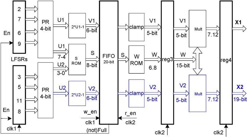
This article has been accepted for inclusion in a future issue of this journal. Content is final as presented, with the exception of pagination.

2                                                                                           IEEE TRANSACTIONS ON INSTRUMENTATION AND MEASUREMENT

                                                                                  Careful timing extraction leads to a reduction in the number of
                                                                                  transmission errors, which is equivalent to an increase in the
                                                                                  system SNR. The theoretical analysis indicates that in a digital
                                                                                  baseband, the relationship between the BER and SNR can be
                                                                                  expressed by
                                                                                                                    √
                                                                                                        BER = Q( SNR)                         (2)
Fig. 1. AWGN channel model.
                                                                                  where Q() is defined in (1).
  In the AWGN model, the transmitted signal s(t) is corrupted                        Another class of communication systems employs modula-
by noise n(t). The model can be expressed by                                      tion schemes for communication over a given portion of spec-
                         r(t) = s(t) + n(t).                                      trum. The modulator at the transmitter performs the function of
                                                                                  mapping the digital sequence into sinusoidal signal waveforms.
   The noise is introduced by the channel, as well as by elec-                    The BER performance of the receivers varies widely, depending
tronic components, including amplifiers at the receiver. This                     on the modulation scheme. For example, assuming that a Gray
type of noise is most often characterized as thermal noise or,                    code is used [8], the relationship between the BER and SNR
statistically, as Gaussian noise. Its probability density function                for the quadrature phase-shift keying (QPSK) modulation can
(pdf) is expressed by                                                             be theoretically characterized by
                           1                                                                           √                   √
                   p(x) = √ e−(x−mx ) /2δ
                                     2    2

                         δ 2π                                                               BER ≈ Q( 2SNR) 1 − 0.5Q( 2SNR) .                  (3)

where mx is the mean, and σ 2 is the variance of the Gaussian                     In such modulation schemes, as the baseband digital signal is
random variable.                                                                  modulated by a complex exponential (sine and cosine waves),
   An important function used to characterize the Gaussian                        two real-valued data streams appear and have to be separately
distribution is the Q function, which represents the area under                   processed. They are referred to as the I (in-phase) channel and
the tail of the Gaussian pdf. Q(x) is used to compute the                         the Q (quadrature) channel.
probability of error in communication systems. Normalized to                         The spread-spectrum technique is yet another implemen-
a zero mean and a unit variance, Q(x) is defined as [8]                           tation of the Shannon law by which the transmitted signal
                                       ∞                                         bandwidth B is much greater than the information bandwidth
                            1
                                            e−t
                                               2
                    Q(x) = √                       /2
                                                        dt.                (1)    C. This excess bandwidth is used as a “coding gain” to protect
                             2π                                                   the signal from the interference caused by multiple users in the
                                       x
                                                                                  same channel, as well as from the intentional jamming.
                                                                                     In all such implementations, the theoretical and practically
A. BER and SNR                                                                    achieved BER versus SNR curves serve to evaluate the overall
                                                                                  capacity and coding gain that is equivalent to the increase in
   A BER is the ratio of the number of incorrect bits and the
                                                                                  the system SNR. It is desirable to quickly obtain the BER
total number of received bits. In general, the BER is a function
                                                                                  performance of a manufactured device in either such case.
of the characteristics of the channel (i.e., amount of noise),
                                                                                     As indicated by (2) and (3), a low BER requires a high SNR.
the type of waveforms used to transmit information over the
                                                                                  In an AWGN communication system, the SNR is determined
channel, the transmitter power, the timing jitter, and the method
                                                                                  by the variance of the AWGN generator. To emulate a low
of demodulation and decoding.
                                                                                  BER system, we usually shrink the distribution of the Gaussian
   An SNR is the fundamental input quantity that determines
                                                                                  generator to achieve a low variance. However, some outputs
the channel capacity C for a given bandwidth B, according to
                                                                                  of the generator must be large enough to produce bit errors.
the fundamental Shannon law, i.e.,
                                                                                  The lowest BER that an AWGN communication system can
                      C = B log2 (1 + SNR).                                       achieve is determined by the tail distribution of the Gaussian
                                                                                  noise or, more specifically, by the maximum output value m of
   In practice, communication system designers balance the                        the noise variable. For a digital system where data “0” and “1”
bandwidth and SNR to maximize the channel capacity for an                         are transmitted, the maximum output of the noise generator is
acceptable BER performance. The BER is related to the SNR                         generally required to be bigger than 0.5 to generate bit errors.
in a way that is impossible to analytically describe in realistic                 The existing hardware AWGN generators (e.g., [5]–[7]) have
systems, and the key role of the tools, such as ours, is to                       a maximum output value of 7. If we use such generators in
discover the relation between the two.                                            baseband transmission, they can only generate a theoretical
   There are several types of communication systems in which                      maximum SNR of 16.9 dB by being scaled by a factor of 14 (see
this balancing act is played in different ways. In baseband                       Section VI-B). Although the 16.9-dB SNR can translate into
transmission, the data and clock are transmitted as digital                       a BER value around 10−12 according to (2), such generators
waveforms. Baseband schemes, such as the commonly used                            are only suitable for exploring the channel behavior at BERs
nonreturn-to-zero CDR encoding, combine clock and data sig-                       down to the range of 10−9 to 10−10 [7]. The distribution near its
nals at the transmitting side and decouple them at the receiver.                  maximum output value of any AWGN generator with bounded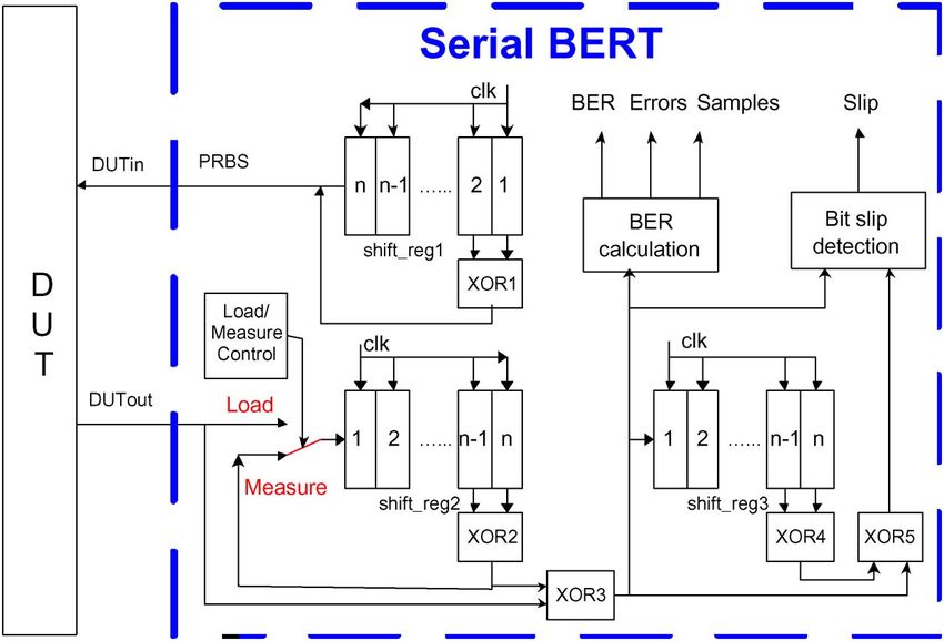
This article has been accepted for inclusion in a future issue of this journal. Content is final as presented, with the exception of pagination.

FAN AND ZILIC: BER TESTING OF COMMUNICATION INTERFACES                                                                                                      3

output is no longer Gaussian, as the ideal Gaussian distribu-
tion is unbounded (the maximum output value is infinity).
Hence, the tail distribution of the existing AWGN generators
needs to be improved for very low BER applications, such
as 10−12 .

B. BER Testing
   All BERTs use the same basic principle: known test patterns
are sent to a design under test (DUT), and the patterns are
compared bit by bit with the output of the DUT after a certain
period of time.
   1) Software Simulation: In the development of a digital
communication system, an initial evaluation of its presili-                       Fig. 2. Block diagram of our BER testing scheme.
con performance is usually performed based on a simplified                               III. O VERVIEW OF O UR BER T ESTING S CHEME
mathematical analysis. Simulation tools like MATLAB and
Simulink [9] are mostly used for this purpose. Since a digital                       To conveniently and cost efficiently test BERs, a new testing
communication system suffers from a wide variety of effects                       scheme is proposed and shown in Fig. 2 [13]. This method
that are difficult to accurately analyze, gaining confidence by                   can facilitate the BER testing and characterization of various
software simulation is an essential part of the early development                 communication interfaces.
stage.                                                                               The proposed solution combines a BERT and an AWGN gen-
   In software simulations, each component of the communica-                      erator in a single FPGA device. The AWGN generator is used to
tion system is built using software models. Each model exhibits                   emulate an AWGN communication channel by adding noise to
the characteristics of its represented component. For instance,                   transmitted streams. The amplitude of the noise is programmed
in MATLAB and Simulink, the DSP Blockset’s Random Source                          according to emulated real noise conditions. Hence, we can
block [10] represents the AWGN noise source. The initial seed                     emulate an AWGN channel in which signals are transmitted
and the variance of the noise generated by the block can be                       with different SNRs. The proposed scheme can easily be set up
specified by users to simulate the AWGN channel in different                      to test the BER performance of a real DUT in real operations
SNR conditions.                                                                   under different SNR conditions.
   2) Hardware Emulation: Although software simulations are                          The DUT can be any communication interface or system that
easy to set up for BER evaluation, they are very time con-                        receives bit or word sequences and then restores the sequences
suming. Execution speed depends on the level of abstraction                       after some signal processing or format changes. Some DUT
of the simulation models. Due to vast amounts of data and                         examples include a transceiver (a transmitter and a receiver),
run-time overhead, simulations are generally not suitable for                     the combination of a modulator and a demodulator, and the
the evaluation of communication systems with a low BER. For                       integration of an encoder and a decoder. Parameterized design
example, if we run a simulation of BER = 10−12 with ten errors                    enables the tester to interface a DUT either in serial, parallel, or
using an average communication model, it would take years                         CDR format. The detailed implementation of the AWGN core
on a personal computer equipped with a 1-GHz Pentium-IV                           and the BERT core is discussed in Sections IV and V.
processor. Moreover, many design variables, such as sam-
pling frequency, digital format, carrier resolution, rounding,                                          IV. AWGN C ORE D ESIGN
and quantization, have to be optimized while satisfying the
best tradeoff between performance and complexity. This would                         AWGN generation methods utilize a variety of statisti-
further lengthen the simulation process.                                          cal techniques. However, they are almost always based on
   To speed up the BER evaluation process and final param-                        transformations or operations performed on uniform random
eter optimization, one can perform direct hardware simula-                        variables [14].
tion, i.e., emulation. As an alternative to simulation, emulation
most commonly utilizes programmable logic devices, such as                        A. Existing Methods of AWGN Generation
FPGAs, to map all or part of a design. With emulation, perfor-
mance evaluation can also take place in hardware. To evaluate                        There are few publications on generating AWGN in digi-
the BER in hardware, a high-speed channel emulator and a                          tal hardware. The most relevant publications in this area are
BERT are essential. In [11], a BER testing solution is presented                  [5]–[7], which implement AWGN generators in FPGAs. These
based on Xilinx RocketIO FPGAs, but it does not include a                         existing solutions are mainly based on the Box–Muller method.
channel emulator. Although a hardware-based emulator com-                            1) CLT Method: According to the CLT, if X is a random
bining a BERT and an AWGN can be found in [12], it needs                          variable of mean mx and standard deviation (SD) σ x , the
software involvement, and the cost is still high. As a result,                    random variable XN , which is defined as
there is an urgent need to develop a low-cost hardware-based
                                                                                                                           N −1
                                                                                                                    1
BER testing scheme that combines an AWGN generator and                                                 XN =         √            (xi − mx )
a BERT.                                                                                                          δx N      i=0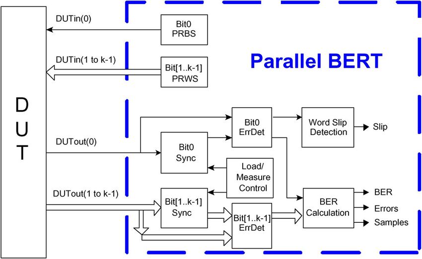
This article has been accepted for inclusion in a future issue of this journal. Content is final as presented, with the exception of pagination.

4                                                                                            IEEE TRANSACTIONS ON INSTRUMENTATION AND MEASUREMENT

tends toward the Gaussian distribution of a zero mean and a unit                   generator proposed in [5], when N = 4, the output rate is only
SD when N tends toward infinity, where xi is N independent                         24.5 MHz, whereas its clock rate reaches 98 MHz.
instances of X.
   The CLT method usually employs an accumulator, which
                                                                                   B. Our Method
greatly slows down the output rate. In addition, implementing
a high-accuracy AWGN generator using this method needs a                              Our method combines the polar method, i.e., Algorithm 2,
large number of samples. Hence, it is not suitable for high-                       with a version of the CLT method [16] in a way that is suitable
speed and high-accuracy applications. The AWGN generator                           for hardware.
in [15] uses this method. It produces one output every 12 clock
cycles by adding 48 random numbers. Its output rate is 1 MHz.                         Algorithm 2: Polar method
   2) Box–Muller Method: The Box–Muller method [17], as                                 1. Do
shown in Algorithm 1, is the most widely known method for                               2. Generate two independent random values U1 and U2 ,
AWGN generation.                                                                            uniformly distributed over [0, 1].
                                                                                        3. Set: V1 = (2∗ U1 ) − 1 and V2 = (2∗ U2 ) − 1.
    Algorithm 1: Box–Muller method                                                      4. Set: S = V12 + V22 .
      1. Generate two independent random values x1 and x2 ,                             5. If S >= 1, go back to line 2.
         uniformly distributed over [0, 1].                                             6. Loop untilS < 1.
      2. Obtain:                                                                       7. Set: W = −2 ln(s)/s.
              f (x1 ) = √ − ln(x1 )                                                     8. Generate two Gaussian variables
              g(x2 ) = 2 cos(2πx2 ).                                                          X1 = V1∗ W
      3. Generate a Gaussian variable                                                         X2 = V2∗ W.
              n = f (x1 )g(x2 ).
                                                                                      As an improvement to the Box–Muller method, the polar
    An FPGA implementation of the Box–Muller method is pro-                        method uses rejection techniques to eliminate the trigonometric
posed in [5], where implementing ln and cos functions requires                     calculations that are usually rather slow [14]. It generates two
careful consideration with regard to the number of recursions                      independently distributed Gaussian variables at the same time,
and relative position of points, as well as the precision of                       which are additionally convenient for applications like QPSK
implementation. The efficient implementation is therefore not                      transmission, where two communication channels are needed.
straightforward.                                                                   The polar algorithm is faster than the Box–Muller algorithm
    Another disadvantage of the Box–Muller method is that it                       because it uses fewer transcendental functions, although it
is not suitable for high m value applications. As indicated in                     throws away, on average, 21% of the numbers generated in the
Algorithm 1, the maximum          √ value of n is determined by
                            √ output                                               Do loop. The proof of validity of the polar method is elaborated
f , as g is bounded by [− 2, + 2]. Since f approaches infinity                     upon in [17].
when values of x1 are close to zero, the maximum output value                         Most importantly, the polar method can easily achieve high
of n is determined by the smallest value of x1 . We express                        maximum output values with little hardware. As indicated in
x1 as 2−l , where l is the number of bits used to represent x1 .                   Algorithm 2, the maximum output value is calculated as a
When l = 32, the maximum output value of the generator is                          logarithm of the minimum value of the square operation of
around 6.7; while l increases to 64, the maximum value can                         random variables U1 and U2 . By contrast, the Box–Muller
only increase to 9.4. Obviously, the hardware cost is high, and                    method directly requires calculation of a logarithm of the
the output speed is limited if we need to achieve a good tail                      random variable x1 . In our implementation, we can produce a
distribution using the Box–Muller method.                                          maximum output value of 53.3 by using only 4 bits (all for the
    Based on the Box–Muller method presented in [5], a com-                        fraction) to represent each uniform random variable (U1 and
mercial AWGN core has been developed [6]. This core is                             U2 in Algorithm 2). To achieve such a high maximum output
only capable of a maximum m value of 4.7. More recently,                           value using the Box–Muller method, we need to use more than
Lee et al. have advanced the Box–Muller method [7] that                            1000 bits to represent the uniform random variable x1 in
increases the maximum m value to 6.7. This improves the tail                       Algorithm 1, which is almost impossible to implement in
distribution of the AWGN generator. However, the price paid                        hardware.
for this improvement is the quadrupled hardware resources,
whereas the speed is halved. While [7] utilizes sophisticated
                                                                                   C. Architecture
statistical test tools to evaluate the AWGN generator, in reality,
the evaluation tool is determined by applications. In most cases,                    1) Polar Method: Based on Algorithm 2, the block diagram
the Q function is good enough for the performance evaluation                       of the polar method for two AWGN generators is developed
as we do in Section IV-D.                                                          and shown in Fig. 3. It can easily be simplified to a single
    3) Mixed Method: As presented in [5], the mixed method                         generator.
combines the CLT method and the Box–Muller method for high                           We use eight independent linear feedback shift registers
accuracy. However, the CLT method slows down the output rate                       (LFSRs) to generate two 4-bit uniformly distributed random
by a factor of N , where N is the number of iterations; therefore,                 variables U1 and U2 . All bits represent fractions; thus, U1 and
the mixed method decreases the AWGN output rate. For the                           U2 are uniformly distributed over [0, 0.9375]. The number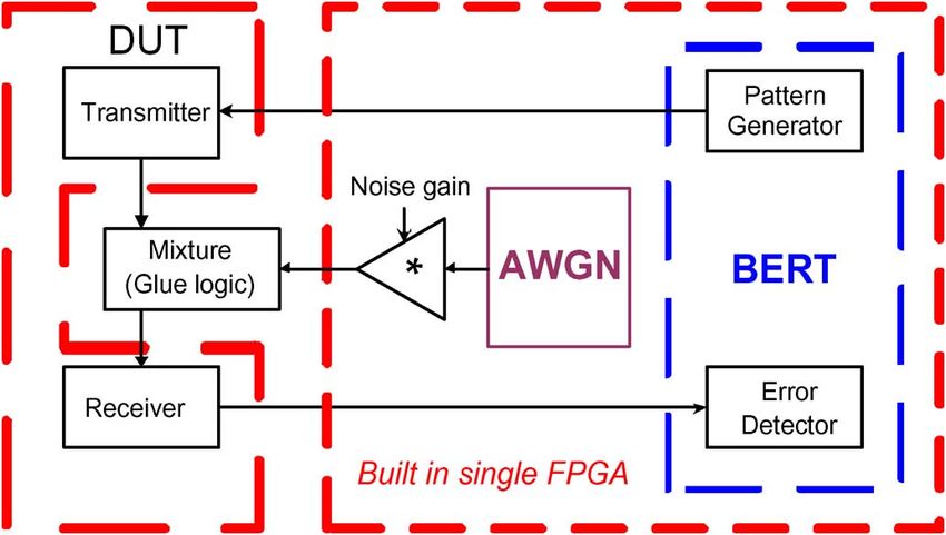
This article has been accepted for inclusion in a future issue of this journal. Content is final as presented, with the exception of pagination.

FAN AND ZILIC: BER TESTING OF COMMUNICATION INTERFACES                                                                                                         5

Fig. 3.   Block diagram of the polar method.

inside the LFSRs represents the length of each LFSR. V1 and
V2 are generated using signed adders. As computing S involves
lots of additions and multiplications, we use a ROM-based
design, where the concatenation of U1 and U2 is set to be
the address, and S is set to be the data stored in the ROM. If
computed S ≥ 1, zero is stored in the ROM.
   As the polar method [17] throws out some data, the Do
loop runs faster than lines 7 and 8 in Algorithm 2. We insert
a synchronizing first-in first-out (FIFO) to achieve a constant
                                                                                     Fig. 4. Our CLT method (N = 4).
output rate. Two clock signals are used in the FIFO: clk1 for
writing and clk2 for reading. Writing is enabled when S is not                                                     TABLE I
equal to 0, whereas reading is always enabled. The LFSRs are                                        Q(x) RELATIVE ERROR OF OUR GENERATORS
disabled when the FIFO is full. The FIFO is 20 bits in width.
By setting the depth of the FIFO to be 16 and clk2 to be half of
clk1, we achieve a constant output rate.
   We also use a ROM-based design to calculate W , where S
denotes the address, and W denotes the data stored in the ROM.
As S is between [0.00390625, 0.99609375], W is between
[53.2835, 0.0886], which can be denoted using 6 bits for the
integer part and 8 bits for the fractional part (6.8).
   Finally, two signed multipliers are used to generate two
Gaussian variables X1 and X2 . Each variable is 19 bits in
width: 1 bit for sign, 6 bits for integer, and 12 bits for fraction
(7.12). The width can be truncated according to applications.
   2) Our CLT Method Implementation: Traditionally, the
CLT method employs an accumulator, which slows down the                              the lengths of all LFSRs; in our case, N equals 51. Statistically
output speed by a factor of N , where N is the number of                             evaluating 251 samples requires a lot of hardware resources and
accumulated variables [5]. We propose our CLT method, as                             time. Our experiments demonstrate that the statistical results of
shown in Fig. 4, which does not exhibit the speed penalty while                      thousands of samples are a good approximation. Table I shows
improving accuracy. Instead of acuminating data in one stage,                        the Q(x) accuracy of our generators with 10 000 and 500 000
the pipelined architecture takes data from previous stages and,                      samples. The samples are taken from a simulator of our AWGN
hence, can output data every clock cycle.                                            generator design and then passed to a UNIX workstation to do
                                                                                     a statistical analysis. Even for the 500 000 samples, it takes the
                                                                                     workstation a whole night to finish the process.
                                                                                        We can see that our method with the parameters shown in
D. Experimental Results
                                                                                     Fig. 3 (simplified to a single generator) implements a high-
  Statistical properties of an AWGN generator should be based                        precision AWGN generator, even with a limited number of
on evaluating samples from at least one period. The period of                        samples. Our CLT method shown in Fig. 4 can further reduce
our generator may reach around 2N , where N is the sum of                            the variation of the distribution. Moreover, note that the relative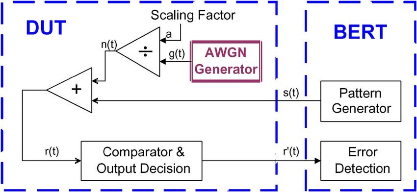
This article has been accepted for inclusion in a future issue of this journal. Content is final as presented, with the exception of pagination.

6                                                                                            IEEE TRANSACTIONS ON INSTRUMENTATION AND MEASUREMENT

Fig. 5. Block diagram of the serial BERT.

error of Q(x) decreases when the number of samples increases.                      XOR3 should be of the same value in each clock cycle. In a
The limited number of samples is the main reason for the error.                    real BER measurement, the output of XOR3 is monitored every
   We also evaluated the accuracy of our AWGN generator by                         clock cycle: if a “1” is detected, a transmission error is counted;
calculating the kurtosis values [18]. Kurtosis characterizes the                   otherwise, the transmission is error free.
relative peakedness or flatness of a distribution compared to the                     In a real communication system, the transmission errors are
Gaussian distribution, which has a theoretical value of 3. Based                   in forms of single-bit errors, error bursts, or bit slips. Bit slips
on the 500 000 samples, we measured a kurtosis of 2.95, which                      result from a bit loss or a bit repeat. If a bit slip happens, only
is 2% less than the required value.                                                the repeated or lost bits should be counted as errors. We employ
                                                                                   a mechanism to distinguish between error bursts and bit slips
                                                                                   and to eliminate false long-term errors.
                      V. BERT C ORE D ESIGN                                           In Fig. 5, the shift register shift_reg3 and the gates XOR 4 and
   As discussed in Section II, the basic concept of a BER                          XOR 5 perform bit slip detection. The solution is based on the
measurement is as follows: The pattern generator sends a data                      fact that the addition or superimposition of two PRBSs shifted
stream to a DUT, and the error detector conducts a bit-by-bit                      in phase relative to each other produces another PRBS [19]. By
comparison of the received signal from the DUT.                                    monitoring the output of XOR 3 and XOR 5, it can be determined
                                                                                   whether a bit slip happens.

A. Serial BERT Design
                                                                                   B. Parallel BERT Design
   A serial BERT sends serial bit sequence patterns to a DUT
and evaluates the output from the DUT. The DUT can be any                             A parallel BERT is used to test communication interfaces
serial digital communication link. The structure of a serial                       that transmit parallel data. The design of the parallel BERT is
BERT is proposed and shown in Fig. 5.                                              based on the serial BERT presented in Section V-A. Basically,
   In this scheme, the shift register shift_reg1 and the gate XOR1                 a k-bit parallel BERT, where k is the width of the parallel
form an LFSR. As the pattern generator of the serial BERT, the                     data (bit0 ∼ bit(k − 1)) can be built using k independent serial
LFSR generates pseudorandom bit sequences (PRBSs). These                           BERTs that have the same load time. The parallel BERT sends
sequences are then sent to the DUT.                                                pseudorandom word sequences (PRWSs) to the DUT. To qual-
   Before a measurement begins, the load/measure switch is                         ify randomness of the generated sequences, the independence
set to be in the load state until the shift_reg2 is fully loaded                   of each of the serial BERTs is very important, which means
with the contents of the shif_reg1. The switch is changed to the                   that the length of the shift registers in each of the serial BERTs
measure state to start the BER measurement. The shift register                     should be different.
shift_reg2, the switch, and the gate XOR2 are used for syn-                           When k independent serial BERTs are directly put together
chronization. They generate a reference pattern by replicating                     to build a parallel BERT, each of the serial BERTs has circuits
the PRBS from the shift_reg1 but delaying the phase. During                        for the load/measure switch control and bit slip detection.
the synchronization process, it is assumed that all the bits are                   However, the circuits for the load/measure switch control of
correctly transmitted.                                                             each bit of the parallel data should change the load/measure
   The gate XOR3 serves as a comparator, comparing the pattern                     state at the same time. Also, the parallel BERT should be
from the DUT with the reference pattern. If the test pattern                       capable of distinguishing between error bursts and word slips
is correctly transmitted by the DUT, then the two inputs of                        instead of bit slips in a serial BERT. Therefore, only one of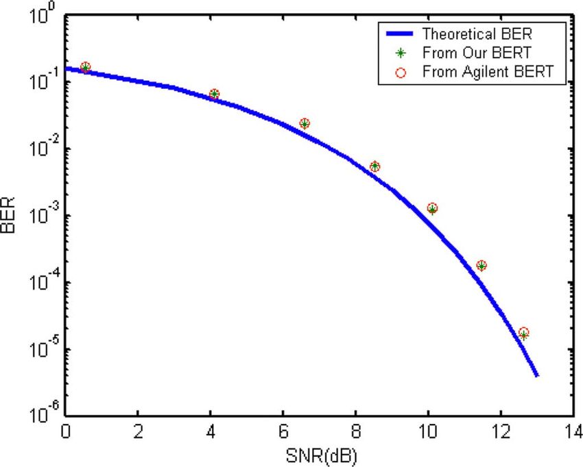
This article has been accepted for inclusion in a future issue of this journal. Content is final as presented, with the exception of pagination.
FAN AND ZILIC: BER TESTING OF COMMUNICATION INTERFACES 7
Fig. 6. Block diagram of the parallel BERT.
TABLE II resources in the FPGA to implement other application-specified
SYNTHESIS RESULTS OF THE AWGN AND BERT
functions in a real BER testing system, such as data storage,
protocol implementations, special test controls, and user logic
circuits.
VI. C ASE S TUDIES
This section presents the applications of the proposed BERT
and AWGN cores for testing of high-speed serial interfaces and
baseband-encoded channels, where they fare favorably with the
the k such control circuits is needed for the switch control and existing methods.
word slip detection. Fig. 6 shows the structure of the proposed
parallel BERT. In the design, the serial BERT control circuitry A. High-Speed Serial Interface Testing
for bit0 is used for the load/measure switch control and the
word slip detection. We test gigabit serial interfaces of the Altera Mercury FPGA
A parallel BERT interfaces a DUT with parallel data, which devices by building our core into the devices. The Mercury
requires lots of connection wires and stringent timing specifi- gigabit transceiver is implemented using the high-speed differ-
cations. The connection interface can be greatly simplified by ential interface (HSDI) to transmit and receive high-speed serial
inserting CDR interfaces between the parallel BERT and the data streams (up to 1.25 Gb/s). Fig. 7 shows the block diagram
DUT. More details about the CDR circuitry are discussed in of one of the eight HSDI transceiver channels (channel 4) of an
Section VI-A. EP1M120F484C7 device [20].
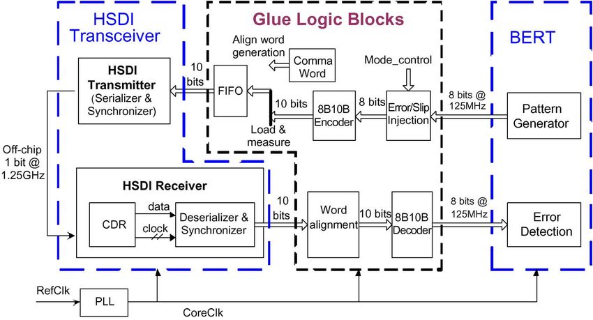
As shown in Fig. 7, the HSDI transmitter includes a synchro-
nizer and a serializer, whereas the receiver includes a clock
C. Synthesis Results
recovery unit, a deserializer, and a synchronizer. The HSDI
The BERT and the previously discussed AWGN designs phase-locked loop circuitry is dedicated to providing clocks for
are built in very high speed integrated circuit hardware de- the transceiver. As the clock is encoded into the data signal in
scription language (VHDL) and can target almost any FPGA the transmitter and recovered at the receiver side, the whole
devices. The synthesis has been done using Quartus II tools by transceiver is often referred to as the CDR interface. Based on
Altera [22]. Table II shows the synthesis results of the AWGN its structure, the setup to test the transceiver is developed and
design and the parallel BERT designs based on the Altera shown in Fig. 8.
Mercury FPGA EP1M120F484C7 device. The embedded sys- In the testing setup, the HSDI transceiver is built by instan-
tem block bits are used to implement ROM-based functions, tiating the Altera block [21]. The data width of the BERT is
such as S and W in Fig. 3. Other logic functions are imple- 8 bits. The glue logic is developed to interface the BERT and
mented in the logic elements (LEs). Each LE contains a four- the transceiver. The Error/Slip Injection block inserts errors or
input lookup table, which can quickly implement any function word slips for the purpose of the demonstration of the BERT
with four variables. The LE also contains a programmable functionalities. The 8B10B encoder encodes the 8-bit sequences
register and a carry chain [20]. to 10-bit sequences to ensure enough bit transitions in the serial
As shown in Table II, the AWGN and the BERT only occupy link for date recovery [23]. A FIFO is used to ensure that
a small part the FPGA device (less than 20%). There are enough there are always data ready for transmission after a test begins.This article has been accepted for inclusion in a future issue of this journal. Content is final as presented, with the exception of pagination.
8 IEEE TRANSACTIONS ON INSTRUMENTATION AND MEASUREMENT
Fig. 7. HSDI transceiver block diagram.
Fig. 8. Testing setup for an HSDI transceiver.
Comma words are inserted at the start of the testing for word
alignment. The 8B10B Decoder recovers the 8-bit PRWSs sent
by the BERT.
The testing setup is implemented in VHDL, targeting the
EP1M120F484C7 device using Quartus II software. The syn-
thesized results are downloaded onto an Altera Mercury HSDI
CDR Demo board. The outputs of the transmitter are connected
to the inputs of the receiver by two subminiature version A
cables.
We obtained a zero BER both from simulations and from
running real tests in the board when no error or bit slip was
Fig. 9. BER testing setup for a digital baseband.
injected. The zero BER experiment results demonstrate the
functional correctness of the HSDI transceiver and the feasi- In the testing setup, the channel is emulated by scaling the
bility of the testing setup. AWGN generator with a zero mean and a unit variance by a
factor of a. In this case, the energy of the noise is
B. Baseband Transmission Testing
No = 2/a2 .
Based on the AWGN model discussed in Section II-A and
our BER testing scheme from Section III, we develop a testing As a result, we have
setup for a digital baseband communication (Fig. 9).
In this system, one is used to transmit data “1,” and zero is SNR = E/N0 = a2 /4.
used to transmit data “0.” Assuming that data 1s and 0s have
equal occurring probabilities, the average energy of transmitted As shown in Fig. 9, the transmitter consists of the pattern
signals is generator, and the receiver consists of the comparator and the
output decision block. If the noise-corrupted signal r(t) is
E = (E0 + E1 )/2 = 0.5. bigger than 0.5 (threshold voltage), r (t) is set to 1; otherwise,This article has been accepted for inclusion in a future issue of this journal. Content is final as presented, with the exception of pagination.
FAN AND ZILIC: BER TESTING OF COMMUNICATION INTERFACES 9
TABLE III needed, our AWGN can accomplish it, as its maximum output
BER MEASUREMENTS FOR A DIGITAL BASEBAND
value reaches 53.
Although the aforementioned experiment is based on testing
a digital baseband system, the proposed BER testing scheme
applies to any AWGN digital transmission system. Further-
more, the AWGN module can be modified to emulate more
complex channels, such as Rayleigh channels.
VII. C ONCLUSION
In this paper, we present a versatile and low-cost BER testing
scheme. The scheme combines a BERT and an AWGN gener-
ator in a single FPGA device, which is suitable for the testing
and characterization of a wide range of signal communication
interfaces. The novel structure of our AWGN generator enables
us to generate a much bigger maximum output value than
the existing solutions (53 versus seven), which is essential for
evaluating the performance of AWGN communication systems
at low BER applications. In addition, our CLT implementation
can speed up the traditional accumulator approach by four
times or more, which is useful to boost the accuracy of any
AWGN generator. Most importantly, the combination of an
AWGN and a BERT in our solution is only a small fraction of
the cost, volume, and energy requirements of a standard-alone
BERT (e.g., [3]) and a standard-alone AWGN generator. Fur-
thermore, the FPGA-based solution makes it easy to interface
with DUTs.
Fig. 10. Measured BER versus theoretical BER. ACKNOWLEDGMENT
The authors would like to thank the reviewers for their
r (t) is 0. Table III lists the test results. The measurements guidance.
were taken while running the testing setup in an Altera Mercury
FPGA board with a clock of 50 MHz. The measurement is first R EFERENCES
done using our BERT and then an Agilent BERT.
[1] E. A. Newcombe and S. Pasupathy, “Error rate monitoring for
Fig. 10 shows the plot of the theoretical BER, the measured digital communications,” Proc. IEEE, vol. 70, no. 8, pp. 805–825,
BERs using our BERT, and an Agilent 81200 BERT as a Aug. 1982.
function of the input SNR. [2] M. Courtoy, “Rapid system prototyping for real-time design validation,”
in Proc. 9th Int. Workshop Rapid Syst. Prototyping, 1998, pp. 108–112.
As indicated in Fig. 10, the measured BER using our BERT [3] Agilent Technologies, Agilent 81200 Data Generator/Analyzer Data
perfectly coincides with that from the expensive Agilent BERT Sheet, 2002.
and is close to the theoretical BER. The plot demonstrates the [4] 48 Gb/s BER Test System Datasheet, Anritsu Corp., Kanagawa, Japan,
2002.
validity of our testing scheme. [5] A. Gazel, E. Boutillon, J. L. Danger, G. Gulak, and H. Lamaari, “Design
In the testing setup, the pattern is generated using an LFSR, and performance analysis of a high speed AWGN communication channel
which produces more 1s than 0s, as all zeros is not a valid emulator,” in Proc. IEEE PACRIM Conf., Aug. 2001, pp. 374–377.
[6] Xilinx Inc., Additive White Gaussian Noise (AWGN) Core v1.0, Oct. 2002.
pattern, whereas all ones is. Therefore, the actual signal energy Production Spec.
is bigger than the theoretical value of 0.5; for example, if the [7] D. Lee, W. Luk, J. Villasenor, and P. Y. K. Cheung, “A Gaussian noise
length of the LFSR is 3, the signal energy it produces is 4/7. We generator for hardware-based simulations,” IEEE Trans. Comput., vol. 53,
no. 12, pp. 1523–1534, Dec. 2004.
take this factor into consideration when calculating the SNRs in [8] J. G. Proakis, Digital Communications. New York: McGraw-Hill, 2001.
Table III. [9] The MathWorks, Inc. [Online]. Available: http://www.mathworks.com
In the aforementioned testing, it takes less than 1 s to gen- [10] Using the Communication Blockset, MathWorks, Inc., Natick, MA,
Jul. 2002.
erate the point at 1.62e-5 BER, whereas software simulations [11] SAPP661: RocketIO Transceiver Bit Error Rate Tester, V2.0, Xilinx, Inc.,
take hours. Furthermore, regardless of the generation scheme, San Jose, CA, Jun. 2003.
going down to low error rates requires many samples just to [12] Nallatech Ltd., Complete Hardware-Based Solution for Bit Error Rate
Testing, Sep. 2002.
exhibit errors—for BER = 10−12 at a 1-GHz data rate, it takes [13] Y. Fan, Z. Zeljko, and M. Chiang, “A versatile high speed bit error
3 h (assuming running 1013 bits to guarantee a 10−12 BER rate testing scheme,” in Proc. Int. Symp. Quality Electron. Des., 2003,
level). In production, the normal practice to qualify the BER pp. 395–400.
[14] M. F. Schollmeyer and W. H. Tranter, “Noise generators for the simulation
performance at such low levels is through extrapolation [24]. of digital communication systems,” in Proc. 24th Annu. Simul. Symp.,
However, if the direct BER measurements at 10−12 or lower are Apr. 1–5, 1991, pp. 264–275.This article has been accepted for inclusion in a future issue of this journal. Content is final as presented, with the exception of pagination.
10 IEEE TRANSACTIONS ON INSTRUMENTATION AND MEASUREMENT
[15] P. Atiniramit, “Design and implementation of an FPGA-based adap- Zeljko Zilic (M’97–SM’07) received the Ph.D. de-
tive filter single-use receiver,” M.S. thesis, Virginia Polytechnic Inst., gree from the University of Toronto, Toronto, ON,
Blacksburg, VA, 1999. Canada, in 1997.
[16] Y. Fan and Z. Zilic, “A novel scheme of implementing high speed AWGN From 1997 to 1998, he was a Member of Techni-
communication channel emulators in FPGAs,” in Proc. Int. Symp. Circuits cal Staff with the FPGA Division, Microelectronics
Syst., May 23–26, 2004, vol. 2, pp. II-877–II-880. Group, Lucent Technologies. He is currently an As-
[17] D. E. Knuth, The Art of Computer Programming. Reading, MA: sociate Professor with McGill University, Montreal,
Addison-Wesley, 1998. QC, Canada. He is also on the Editorial Board of the
[18] D. Ruppert, “What is kurtosis? An influence function approach,” Amer. Journal of Multiple-Valued Logic and Soft Comput-
Stat., vol. 41, no. 1, pp. 1–5, Feb. 1987. ing and the International Journal of Software and
[19] R. Kiefer, Test Solutions for Digital Networks. Heidelberg, Germany: Information Technologies. He has published more
Huthig GmbH, 1998. than 100 research papers and coauthored the book Verification by Error
[20] Altera Corp., Mercury Programmable Logic Device Family Data Sheet, Modeling (Kluwer, 2003). He is the holder of four patents in the area of clock
Jan. 2003. and power management. His current research interests include various aspects
[21] Altera Corp., Mercury Gigabit Transceiver MegaCore Function User of system design, test, and verification.
Guide, Feb. 2002. Prof. Zilic has served as a member of Technical Program Committees for
[22] Introduction to Quartus II Manual, Altera Corp., San Jose, CA, Jul. 2003. the ACM International Symposium on FPGAs, the IEEE International Test
[23] Altera Corp., 8B10B Encoder/Decoder MegaCore Function User Guide, Conference, the Midwest Circuits and Systems Symposium, and the Electronic
Dec. 2002. Circuits and Systems Conference. He has been granted the Chercheur Strate-
[24] Y. Fan, Y. Cai, L. Fang, A. Verma, B. Burcanowski, Z. Zilic, and S. Kumar, gique Research Chair from the Province of Quebec. He was a recipient of
“An accelerated jitter tolerance test technique on ATE for 1.5 GB/s and the Myril B. Reed Best Paper Award from the IEEE International Midwest
3 GB/s serial-ATA,” in Proc. IEEE ITC, 2006, pp. 1–10. Symposium on Circuits and Systems in 2001, a Best Paper Award from the
Design and Verification Conference in 2005, and several honorary mention
awards. For his undergraduate teaching, the National Council of Deans of
Yongquan Fan (S’07) received the B.S. degree in Engineering and Applied Science and Sandford Fleming Foundation awarded
electrical engineering from Beijing University of him with the Wighton Fellowship in 2006. As a Vice President of Research
Aeronautics and Astronautics, Beijing, China, in and Development, he helped start up Monroi, Inc., which is a company that
1991 and the M.S. degree in electrical engineering was given an Entrepreneur of the Year Award by the St. Laurent Chamber of
from McGill University, Montreal, QC, Canada, in Commerce in 2004.
2003. He is currently working toward the Ph.D.
degree at McGill University.
He is also a Staff Engineer with the Test Engineer-
ing of Storage Peripheral Group, LSI Corporation,
where he is developing test solutions for high-speed
mixed signal products. His research concentrates on
accelerating BER and jitter testing.You can also read