LPDDR4 Memory Interface Module - Lattice Radiant Software User Guide - FPGA-IPUG-02154-1.1
←
→
Page content transcription
If your browser does not render page correctly, please read the page content below
LPDDR4 Memory Interface Module - Lattice
Radiant Software

User Guide

FPGA-IPUG-02154-1.1

June 2021
LPDDR4 Memory Interface Module - Lattice Radiant Software
User Guide

Disclaimers
Lattice makes no warranty, representation, or guarantee regarding the accuracy of information contained in this document or the suitability of its
products for any particular purpose. All information herein is provided AS IS and with all faults, and all risk associated with such information is entirely
with Buyer. Buyer shall not rely on any data and performance specifications or parameters provided herein. Products sold by Lattice have been
subject to limited testing and it is the Buyer's responsibility to independently determine the suitability of any products and to test and verify the
same. No Lattice products should be used in conjunction with mission- or safety-critical or any other application in which the failure of Lattice’s
product could create a situation where personal injury, death, severe property or environmental damage may occur. The information provided in this
document is proprietary to Lattice Semiconductor, and Lattice reserves the right to make any changes to the information in this document or to any
products at any time without notice.

                   © 2020-2021 Lattice Semiconductor Corp. All Lattice trademarks, registered trademarks, patents, and disclaimers are as listed at www.latticesemi.com/legal.
      All other brand or product names are trademarks or registered trademarks of their respective holders. The specifications and information herein are subject to change without notice.

2                                                                                                                                                                 FPGA-IPUG-02154-1.1
LPDDR4 Memory Interface Module - Lattice Radiant Software
User Guide
Contents
Acronyms in This Document ................................................................................................................................................. 5
1. Introduction .................................................................................................................................................................. 6
1.1. Quick Facts .......................................................................................................................................................... 6
1.2. Features .............................................................................................................................................................. 6
1.3. Conventions ........................................................................................................................................................ 7
1.3.1. Nomenclature................................................................................................................................................. 7
1.3.2. Signal Names .................................................................................................................................................. 7
2. Functional Description .................................................................................................................................................. 8
2.1. Overview ............................................................................................................................................................. 8
2.2. Signal Description .............................................................................................................................................. 10
2.3. Attribute Summary............................................................................................................................................ 13
2.4. DDR Memory Primitives .................................................................................................................................... 14
2.4.1. Input/Output DELAY ..................................................................................................................................... 15
2.4.2. IDDR/ODDR .................................................................................................................................................. 16
2.4.3. ODDRX4DQS ................................................................................................................................................. 17
2.4.4. Memory Output DDR Primitives for Tristate Output Control ...................................................................... 17
2.4.5. OSHX4 ........................................................................................................................................................... 18
2.4.6. DDRDLL ......................................................................................................................................................... 18
2.4.7. ECLKDIV ........................................................................................................................................................ 19
2.4.8. ECLKSYNC ..................................................................................................................................................... 19
2.4.9. DQSBUF_IVREF ............................................................................................................................................. 19
2.5. Clock Synchronization Logic .............................................................................................................................. 20
2.6. Data Input/Output Path .................................................................................................................................... 21
2.6.1. Write Data access ......................................................................................................................................... 23
2.6.2. Read Data access .......................................................................................................................................... 23
2.6.3. DQS Read Training ........................................................................................................................................ 24
2.7. Command/Address Path ................................................................................................................................... 25
2.8. Training Support................................................................................................................................................ 26
2.8.1. Command Bus Training ................................................................................................................................ 26
3. Core Generation, Simulation, and Validation ............................................................................................................. 27
3.1. Licensing the IP.................................................................................................................................................. 27
3.2. Generation and Synthesis ................................................................................................................................. 27
3.3. Running Functional Simulation ......................................................................................................................... 30
Appendix A. Resource Utilization ....................................................................................................................................... 32
References .......................................................................................................................................................................... 33
Technical Support Assistance ............................................................................................................................................. 34
Revision History .................................................................................................................................................................. 35
© 2020-2021 Lattice Semiconductor Corp. All Lattice trademarks, registered trademarks, patents, and disclaimers are as listed at www.latticesemi.com/legal.
All other brand or product names are trademarks or registered trademarks of their respective holders. The specifications and information herein are subject to change without notice.
FPGA-IPUG-02154-1.1 3LPDDR4 Memory Interface Module - Lattice Radiant Software
User Guide
Figures
Figure 2.1. LPDDR4 Memory Interface Application ..............................................................................................................8
Figure 2.2. DDR Memory Interface Module Block Diagram (No PLL Instance) .....................................................................9
Figure 2.3. Reference Guide for the Primitive Library ........................................................................................................14
Figure 2.4. DELAYA Block Diagram......................................................................................................................................15
Figure 2.5. DELAYB Block Diagram ......................................................................................................................................15
Figure 2.6. OUTDELAYA Block Diagram...............................................................................................................................16
Figure 2.7. IDDRX2DQ Block Diagram .................................................................................................................................16
Figure 2.8. ODDRX4DQ Block Diagram ...............................................................................................................................17
Figure 2.9. ODDRX4DQS Block Diagram..............................................................................................................................17
Figure 2.10. TSHX4DQ Block Diagram .................................................................................................................................17
Figure 2.11. TSHX4DQS Block Diagram ...............................................................................................................................18
Figure 2.12. OSHX4 Block Diagram .....................................................................................................................................18
Figure 2.13. DDRDLL Block Diagram ...................................................................................................................................18
Figure 2.14. ECLKDIV Block Diagram ...................................................................................................................................19
Figure 2.15. ECLKSYNC Block Diagram ................................................................................................................................19
Figure 2.16. DQSBUF_IVREF Block Diagram........................................................................................................................19
Figure 2.17. Clock Synchronization Logic Block Diagram ....................................................................................................20
Figure 2.18. Clock Synchronization Logic Block Diagram ....................................................................................................21
Figure 2.19. Data Input/Output Path Block Diagram ..........................................................................................................22
Figure 2.20. Write BL16 timing diagram .............................................................................................................................23
Figure 2.21. Write BL16 timing diagram with added 2nCK latency ....................................................................................23
Figure 2.22. Read BL16 timing diagram (rd_clksel_i =4’h0) ................................................................................................23
Figure 2.23. Read BL16 timing diagram (rd_clksel_i =4’hF) ................................................................................................24
Figure 2.24. Command/Address Path Block Diagram .........................................................................................................25
Figure 2.25. Command/Address Path Timing diagram .......................................................................................................26
Figure 2.26. LPDDR4 Memory VREFCA Programming Timing Diagram ................................................................................26
Figure 2.27. Sending/Capture a CA Pattern Timing Diagram ..............................................................................................26
Figure 3.1. Module/IP Block Wizard ...................................................................................................................................27
Figure 3.2. Configure Block of DDR Memory Module.........................................................................................................28
Figure 3.3. Check Generating Result ...................................................................................................................................28
Figure 3.4. Simulation Wizard .............................................................................................................................................30
Figure 3.5. Adding and Reordering Source .........................................................................................................................30
Figure 3.6. Simulation Waveform .......................................................................................................................................31
Tables
Table 1.1. Quick Facts ...........................................................................................................................................................6
Table 2.1. LPDDR4 Memory Interface Module Signal Description .....................................................................................10
Table 2.2. Attribute Table ...................................................................................................................................................13
Table 3.1. Generated File List .............................................................................................................................................29
Table A.1. Resource Utilization ...........................................................................................................................................32
© 2020-2021 Lattice Semiconductor Corp. All Lattice trademarks, registered trademarks, patents, and disclaimers are as listed at www.latticesemi.com/legal.
All other brand or product names are trademarks or registered trademarks of their respective holders. The specifications and information herein are subject to change without notice.
4 FPGA-IPUG-02154-1.1LPDDR4 Memory Interface Module - Lattice Radiant Software
User Guide
Acronyms in This Document
A list of acronyms used in this document.
Acronym Definition
DDR Double Data Rate
FPGA Field Programmable Gate Array
LPDDR Low-Power Double Data Rate
LSE Lattice Synthesis Engine
© 2020-2021 Lattice Semiconductor Corp. All Lattice trademarks, registered trademarks, patents, and disclaimers are as listed at www.latticesemi.com/legal.
All other brand or product names are trademarks or registered trademarks of their respective holders. The specifications and information herein are subject to change without notice.
FPGA-IPUG-02154-1.1 5LPDDR4 Memory Interface Module - Lattice Radiant Software
User Guide
1. Introduction
The Lattice Semiconductor Low Power Double Data Rate 4 (LPDDR4) Memory Interface Module generates a module
that can be used to interface to an LPDDR Memory and includes a bidirectional port and the associated clocking
scheme.
1.1. Quick Facts
Table 1.1 presents a summary of LPDDR4 Memory Module.
Table 1.1. Quick Facts
IP Requirements Supported FPGA Family CertusPro™-NX
Targeted Devices LFCPNX-100
Resource Utilization Supported User Interface LPDDR4, Native interface – see Signal Description section.
Resources See Table A.1.
Lattice Implementation Lattice Radiant™ software 3.0
Lattice Synthesis Engine (LSE)
Synthesis
Design Tool Support Synopsys® Synplify Pro® for Lattice
For a list of supported simulators, see the Lattice Radiant software user
Simulation
guide.
1.2. Features
Key features of Low Power Double Data Rate 4 (LPDDR4) Memory Module include:
Supports LPDDR4 memory interface
Frequency Supported: 200, 250, 300, 350, 400, 533 MHz
Supports 8:1 (X4) gearing ratio
Write Leveling support for LPDDR4
DQ-DQS skew optimization for Write Training
Dynamic valid window optimization (Read and Write Path)
Configurable number of chip selects
Configurable number of clocks
Internal programmable Vref
Includes PLL for clock generation
© 2020-2021 Lattice Semiconductor Corp. All Lattice trademarks, registered trademarks, patents, and disclaimers are as listed at www.latticesemi.com/legal.
All other brand or product names are trademarks or registered trademarks of their respective holders. The specifications and information herein are subject to change without notice.
6 FPGA-IPUG-02154-1.1LPDDR4 Memory Interface Module - Lattice Radiant Software
User Guide
1.3. Conventions
1.3.1. Nomenclature
The nomenclature used in this document is based on Verilog HDL.
1.3.2. Signal Names
Signal names that end with:
_n are active low
_i are input signals
_o are output signals
_io are bi-directional input/output signals
© 2020-2021 Lattice Semiconductor Corp. All Lattice trademarks, registered trademarks, patents, and disclaimers are as listed at www.latticesemi.com/legal.
All other brand or product names are trademarks or registered trademarks of their respective holders. The specifications and information herein are subject to change without notice.
FPGA-IPUG-02154-1.1 7LPDDR4 Memory Interface Module - Lattice Radiant Software
User Guide
2. Functional Description
2.1. Overview
LPDDR4 Memory Interface Module instantiates the DDR primitives to implement the necessary features for interfacing
with LPDDR4 memory devices with data rates up to 1066Mbps. This module is used to pass commands and data signals
from the FPGA fabric operating in system clock to the LPDDR4 memory device operating in the high-speed DDR clock.
The LPDDR4 Memory Interface is operating on 8:1 gearing ratio or X4 gearing mode which means:
The DDR clock (ddr_ck_o) frequency is 4x the system clock (sclk_o) frequency
The bit width of data signal in system clock domain is equivalent to DDR DQ/DQS/DMI bit width x 8. Thus, it takes 4
ddr_ck_o cycles to transfer the data to/from system clock domain. Note that data is transferred on both ddr_ck_o
edges.
On the other hand, bit width of command/address signal in system clock domain is equivalent to DDR
CKE/CS/CA/ODT bit width x 4. These signals are shifted out on ddr_ck_o falling edge and the external memory
sample these on the rising edge.
This module is designed to be used with a memory controller as show in Figure 2.1. The memory controller organizes
the command and data signals in system clock domain and this module converts them to high-speed LPDDR4 signaling.
LPDDR4 Memory Interface
DDR Memory Clock (CK)
LPDDR4 Memory Controller (MC)
Clock Enable (CKE)
LPDDR4 Memory Device
Chip Select (CSN)
Command/Address Inputs (CA)
System DDR
Clock Clock
Domain On-Die Termination (ODT) Domain
Input/Output Data Bus (DQ)
PLL
Input/Output Data Strobe (DQS)
Data Mask Inversion (DMI)
Figure 2.1. LPDDR4 Memory Interface Application
© 2020-2021 Lattice Semiconductor Corp. All Lattice trademarks, registered trademarks, patents, and disclaimers are as listed at www.latticesemi.com/legal.
All other brand or product names are trademarks or registered trademarks of their respective holders. The specifications and information herein are subject to change without notice.
8 FPGA-IPUG-02154-1.1LPDDR4 Memory Interface Module - Lattice Radiant Software
User Guide
The top level block diagram of the LPDDR4 Memory Interface Module is shown in Figure 2.2. This shows that the bit
width of command/address path signals in the memory controller side is 4x of the bit width of the corresponding
memory the device-side signals. While bit width of data I/O path signals in the memory controller side is 8x of the bit
width of the memory the device-side signals.
The command bus signals have configurable output delay signals per bit (Per Bit Delay Adj.) to support command bus
training. The data I/O path on the other hand have two levels of delay adjustment: the Per DQS Grp. Delay Adj. and the
Per Bit Delay Adj.
[Memory Controller side] Command/Address Path [Memory Device side]
ck_oe_n_i
ddr_ck_o
8'hAA ODDRX4 DELAYB (differential pair)
cke_i[3:0] ddr_cke_o
OSHX4 DELAYB
reset_n_i ddr_reset_n_o
Register
ca_oe_n_i
odt_i[3:0] ddr_odt_o
OSHX4 DELAYB
cs_i[3:0] ddr_cs_o
OSHX4 DELAYA
[rep. (6)x] [rep. (6)x]
ca_i[23:0] ddr_ca_o[5:0]
OSHX4 DELAYA
Data Input/Output Path
dq_oe_n_i[DW/2-1:0] [rep. (DW/8)x]
TSHX4DQ
[rep. (DW/8)x]
dmi_i[DW-1:0] [rep. (DW/8)x] ddr_dmi_io
ODDRX4DQ OUTDELAYA
[rep. (DW)x] [DW/8-1:0]
dq_i[8*DW-1:0] [rep. (DW)x] ddr_dq_io
ODDRX4DQ OUTDELAYA
[DW-1:0]
dqs_grp_vref_i[6:0]
IVREF
Per Bit Delay Adj.
dqsw270 [rep. (DW/8)x]
dmi_o[DW-1:0] [rep. (DW/8)x]
IDDRX4DQ DELAYA
[rep. (DW)x] [rep. (DW)x]
dq_o[8*DW-1:0]
IDDRX4DQ DELAYA
rdpntr/wrpntr
dqsr90
data_valid_o[DW/8-1:0]
sclk_o
sclk [rep. (DW/8)x]
Clock Sync. DQSBUFA
Logic
Rd Section
eclk_i ECLKDIV
ECLKSYNC FIFO Control
dllcode
DDRDLL eclk Wr Section
Per DQS Grp. Delay Adj.
ddr_dqs_io
Other DQSBUF signals
[DW/8-1:0]
dqs_oe_n_i[DW/2-1:0] [rep. (DW/8)x] (differential pair)
TSHX4DQS
dqsw
dqs_i[DW-1:0] [rep. (DW/8)x]
ODDRX4DQS OUTDELAYA
Figure 2.2. DDR Memory Interface Module Block Diagram (No PLL Instance)
© 2020-2021 Lattice Semiconductor Corp. All Lattice trademarks, registered trademarks, patents, and disclaimers are as listed at www.latticesemi.com/legal.
All other brand or product names are trademarks or registered trademarks of their respective holders. The specifications and information herein are subject to change without notice.
FPGA-IPUG-02154-1.1 9LPDDR4 Memory Interface Module - Lattice Radiant Software
User Guide
2.2. Signal Description
Table 2.1 describes theLPDDR4 Memory Interface Module signals. The signals are grouped as follows:
Clock and Reset – As the group name implies, these are clock and reset signals. This also includes the signal that
controls the clock and indicates the clock ready status. Please refer to Clock Synchronization Logic section for more
information on this group.
User Interface – The LPDDR4 Controller use this group to control the LPDDR4 Interface group in implementing the
LPDDR4 protocol. Please refer to Data Input/Output Path and Command/Address Path sections for more
information on this group.
Per DQS Group Delay Adjustment – Implements delay adjustment for DQS-DQ read data path, DQS-DQ write data
path and CK-DQS write data path (write leveling). A DQS group is composed of 8-bit of DQ and the corresponding
DQS and DMI bit. Please refer to Training Support section for more information on this group.
Per Bit Delay Adjustment – Implements delay per bit adjustment for the command bus (CS/CA). Please refer to
Command Bus Training section for more information on this group.
Note: We are planning to remove the per bit delay adjustment on DQ/DMI signal
Table 2.1. LPDDR4 Memory Interface Module Signal Description
Pin Name Direction Width (Bits)1 Description
Clock and Reset
pll_refclk_i In 1 Reference clock input for PLL
pll_lock_o Out 1 Signal from PLL indicating stable clock condition
rst_i In 1 Active HIGH reset signal
sync_clk_i In 1 Input clock that drives the soft logic that controls the PLL instance. You
should not connect to sclk_o because the sclk_o is stopped during clock
frequency change. If the PLL Reference Clock from Pin attribute is
checked, you should not connect this to pll_refclk_i.
sclk_o Out 1 Output clock with frequency equal to DDR clock divided by 4
ddr_clk_sel_i In 3 Selects the DDR clock frequency when performing clock frequency
change. This signal must remain stable when clock_update_i asserts
until ready_o negates.
0: Operating frequency – DDR Memory Frequency attribute
1: Command Bus Training frequency – 50 MHz
dll_update_en_i In 1 Enables DLL update during clock frequency change. DLL update has long
delay. This it is recommended to only perform DLL update on the final
clock frequency change of command bus training.
clk_update_i In 1 A transition from LOW to HIGH triggers the clock frequency change
according to ddr_clk_sel_i signal. This signal must remain stable until
ready_o goes HIGH again.
ddr_ck_en_i In 1 Enables the clock toggling of ddr_ck_o
ready_o Out 1 Indicates internal DDR clock and sclk_o are stable and ready to operate.
This signal negates during clock frequency change and asserts again when
both DDR clock and sclk_o are valid for the new frequency setting.
LPDDR4 User Interface
ck_oe_n_i In 1 Tristate control port for CK/CKE
cke_i In 4 Clock Enable input
ca_oe_n_i In 1 Tristate control port for CS/CA/ODT
cs_i In 4 Chip Select input
ca_i In 24 Command/Address input
odt_i In 4 On-die Termination input
reset_n_i In 1 DDR Reset input
write_dqs_oe_n_i In DW/2 Tristate control port for DQS
write_dqs_i In DW Parallel DQS input
write_dq_oe_n_i In DW/2 Tristate control port for DQ/DMI.
© 2020-2021 Lattice Semiconductor Corp. All Lattice trademarks, registered trademarks, patents, and disclaimers are as listed at www.latticesemi.com/legal.
All other brand or product names are trademarks or registered trademarks of their respective holders. The specifications and information herein are subject to change without notice.
10 FPGA-IPUG-02154-1.1LPDDR4 Memory Interface Module - Lattice Radiant Software
User Guide
Pin Name Direction Width (Bits)1 Description
write_dmi_i In DW Data Mask inversion input.
write_dq_i In 8*DW Parallel data bus input.
read_dqs_ie_i In 4 Read enable signal for capturing the incoming read BL16. Each bit
captures the DQ/DMI for the corresponding ddr_ck_o cycle.
Please refer to DQS Read Training for more information.
read_dmi_o Out DW Data Mask Inversion output.
read_dq_o Out 8*DW Parallel data bus output.
read_data_valid_o Out DW/8 Data valid flag for READ mode.
DQS Group Training
pause_i In 1 Set this to 1 to stop the DQSBUF-generated internal clocks when
updating rd_clksel_i and the delay codes. This is to avoid metastability.
rd_clksel_i In 4 Used to select read clock source and polarity control.
[1:0]: selects the 0, 45, 90, and 135 (2b00 to 2b11 respectively)
degree paths from the DQS write section delay cell.
[2] = 1b0: use inverted clock
[2] = 1b1: use non-inverted clock – adds 180 degree shift
[3] = 1b0: bypasses the register in the read enable path
[3] = 1b1: selects the register in the read enable path
Please refer to DQS Read Training for more information.
burst_det_sclk_o Out DW/8 Clock generated using burst_det_o.
dqs_grp_vref_i In 7 Controls I/O drive strength of data I/O path signals by changing the
internal voltage reference.
rd_load_n_i In DW/8 Asynchronously resets the delay code according to the Dynamic Margin
Control attribute for DQS-DQ skew compensation in read data path.
rd_move_i In DW/8 At rising edge, it changes (+/- 1) the delay code according to rd_dir_i
signal for DQS-DQ in read data path.
rd_dir_i In DW/8 Controls the direction of delay code change for DQS-DQ skew
compensation in read data path.
‘0’ to increase and ‘1’ to decrease the delay code.
rd_cout_o4 Out DW/8 Margin test output flag to indicate the under-flow or over-flow in delay
code for DQS-DQ skew compensation in read data path.
wr_load_n_i In DW/8 Reset the delay code according to the Dynamic Margin Control
attribute for DQS-DQ skew compensation in write data path.
A pulse (Low-High-Low) in wr_move_i is needed to perform reset.
wr_move_i In DW/8 At rising edge, it changes (+/- 1) the delay code according to wr_dir_i
signal for DQS-DQ skew compensation in write data path.
wr_dir_i In DW/8 Controls the direction of delay code change for DQS-DQ skew
compensation in write data path.
‘0’ to increase and ‘1’ to decrease the delay code.
wr_cout_o4 Out DW/8 Margin test output flag to indicate the under-flow or over-flow in delay
code for DQS-DQ skew compensation in write data path.
wrlvl_load_n_i In DW/8 Asynchronously resets the delay code to factory default value for CK-
DQS skew compensation – Write Leveling.
Note: The reset value is 0 (subject for revision).
wrlvl_move_i In DW/8 At rising edge, it changes (+/–1) the delay code according to the
direction set by wrlvl_dir_i for CK-DQS skew compensation – Write
Leveling.
wrlvl_dir_i In DW/8 Controls the direction of delay code change for CK-DQS skew
compensation (Write Leveling) in write data path.
‘0’ to increase and ‘1’ to decrease the delay code.
wrlvl_cout_o4 Out DW/8 Margin test output flag to indicate the under-flow or over-flow for CK-
DQS skew compensation – Write Leveling.
© 2020-2021 Lattice Semiconductor Corp. All Lattice trademarks, registered trademarks, patents, and disclaimers are as listed at www.latticesemi.com/legal.
All other brand or product names are trademarks or registered trademarks of their respective holders. The specifications and information herein are subject to change without notice.
FPGA-IPUG-02154-1.1 11LPDDR4 Memory Interface Module - Lattice Radiant Software
User Guide
Pin Name Direction Width (Bits)1 Description
dqwl_o4 Out DW Data output of write leveling.
Per Bit DQ/DMI Training
dq_out_adj_load_n_i2 In DW DQ output delay per bit adjustment load signal.
dq_out_adj_move_i2 In DW DQ output delay per bit adjustment signal.
dq_out_adj_dir_i2 In DW DQ output delay per bit adjustment direction signal.
dq_out_adj_cout_o2, 4 Out DW DQ output delay per bit adjustment cout signal.
dmi_out_adj_load_n_i2 In DW/8 DMI output delay per bit adjustment load signal.
dmi_out_adj_move_i2 In DW/8 DMI output delay per bit adjustment move signal.
dmi_out_adj_dir_i2 In DW/8 DMI output delay per bit adjustment direction signal.
dmi_out_adj_cout_o2, 4 Out DW/8 DMI output delay per bit adjustment cout signal.
dqs_out_adj_load_n_i2 In DW/8 DQS output delay per bit adjustment load signal.
dqs_out_adj_move_i2 In DW/8 DQS output delay per bit adjustment move signal.
dqs_out_adj_dir_i2 In DW/8 DQS output delay per bit adjustment direction signal.
dqs_out_adj_cout_o2, 4 Out DW/8 DQS output delay per bit adjustment cout signal.
dq_in_adj_load_n_i3 In DW DQ input delay per bit adjustment load signal.
dq_in_adj_move_i3 In DW DQ input delay per bit adjustment signal.
dq_in_adj_dir_i3 In DW DQ input delay per bit adjustment direction signal.
dq_in_adj_cout_o3, 4 Out DW DQ input delay per bit adjustment cout signal.
dmi_in_adj_load_n_i3 In DW/8 DMI input delay per bit adjustment load signal.
dmi_in_adj_move_i3 In DW/8 DMI input delay per bit adjustment move signal.
dmi_in_adj_dir_i3 In DW/8 DMI input delay per bit adjustment direction signal.
dmi_in_adj_cout_o3, 4 Out DW/8 DMI input delay per bit adjustment cout signal.
Command Bus Training
cs_adj_load_n_i3 In 1 CS delay adjustment load signal.
cs_adj_move_i3 In 1 CS delay adjustment signal.
cs_adj_dir_i3 In 1 CS delay adjustment direction signal.
cs_adj_cout_o3, 4 Out 1 CS delay adjustment cout signal.
ca_adj_load_n_i3 In 6 CA delay per bit adjustment load signal.
ca_adj_move_i3 In 6 CA delay per bit adjustment signal.
ca_adj_dir_i3 In 6 CA delay per bit adjustment direction signal.
ca_adj_cout_o3, 4 Out 6 CA delay per bit adjustment cout signal.
LPDDR4 Interface
ddr_ck_o Out 1 LPDDR4 Clock output (CK).
This becomes differential pair signal at the FPGA IO pad.
ddr_cke_o Out 1 LPDDR4 Clock Enable output (CKE).
ddr_cs_o Out 1 LPDDR4 Chip Select output (CS).
ddr_ca_o Out 6 LPDDR4 Command/Address output (CA).
ddr_odt_o Out 1 LPDDR4 On-Die Termination Control output (ODT).
ddr_reset_n_o Out 1 LPDDR4 Reset output (RESET_n)
ddr_dq_io In/Out DW LPDDR4 Data Input/Output (DQ).
ddr_dqs_io In/Out DW/8 LPDDR4 Data Strobe Input/Output (DQS).This signal becomes
differential pair at the IO FPGA pad.
ddr_dmi_io In/Out DW/8 LPDDR4 Data Mask Inversion Input/Output (DMI).
Notes:
1. DW = Data Bus Width attribute
2. These signals are connected to OUTDELAYA primitive, refer to the Signal Description section for the signal description.
3. These signals are connected to DELAYA primitive, refer to the Signal Description section for the signal description.
4. All the *cout_o and dqwl_o signals must be registered directly before driving other logic.
© 2020-2021 Lattice Semiconductor Corp. All Lattice trademarks, registered trademarks, patents, and disclaimers are as listed at www.latticesemi.com/legal.
All other brand or product names are trademarks or registered trademarks of their respective holders. The specifications and information herein are subject to change without notice.
12 FPGA-IPUG-02154-1.1LPDDR4 Memory Interface Module - Lattice Radiant Software
User Guide
2.3. Attribute Summary
Table 2.2. Attribute Table
Attribute Selectable Values Default Dependency on Other Attributes
General Tab
General Group
I/O Buffer Type LVSTL_I, LVSTL_II LVSTL_I
Gearing Ratio 8:1 8:1 Display Information only
Data Bus Width 16, 32, 64 16 —
Number of DQS Group Calculated = (Data Bus N/A Data Bus Width
Width)/8
Enable Dynamic Margin Control on Checked, Unchecked Checked Display Information only
Clock Delay
Enable Per Bit Delay Adjustment on Checked, Unchecked Unchecked —
DQS Group
Enable Per Bit Delay Adjustment on Checked, Unchecked Checked —
CA Group
Clock Settings Group
DDR Memory Frequency (MHz) 200, 250, 300, 350, 400, 400 —
533
System Clock Frequency (MHz) Calculated = (DDR N/A Display Information only
Memory Frequency)
/Gearing Ratio
Enable PLL Checked Checked Display Information only
PLL Input Frequency* 10 – 800 100 —
PLL Reference Clock from Pin Checked, Unchecked Unchecked —
PLL Reference Clock I/O Type LVSTL_I, LVSTL_II, LVSTL_I PLL Reference Clock from I/O Pin are both
LVSTLD_I, LVSTLD_II, Checked
LVTTL33, LVCMOS33,
LVCMOS25, LVCMOS18,
LVCMOS18H,
HSTL15D_I, LVCMOS15,
LVCMOS15H,
LVCMOS12,
LVCMOS12H,
LVCMOS10H,
LVCMOS10,
LVCMOS10R
Clock Output Tolerance (%) 0.0, 0.1, 0.2, 0.5, 1.0, 0.1 ‘Enable PLL’ is Checked
2.0, 5.0, 10.0
DDR Memory Actual Frequency Calculated N/A Display Information only
(MHz)
Clock/Address/Command
Number of Clocks 1, 2, 4 1
Address Width 6 6 Display Information only
Number of Chip Selects 1, 2, 4 1
Number of Chip ODT 1 1 Display Information only
Dynamic Margin Control
DQS Read Delay Adjustment Enable Checked, Unchecked Unchecked Enable Dynamic Margin Control on Clock
Delay is Checked
DQS Read Delay Adjustment Sign POSITIVE, POSITIVE DQS Read Delay Adjustment Enable is
COMPLEMENT Checked
DQS Read Delay Adjustment Value 0 to 255 0
© 2020-2021 Lattice Semiconductor Corp. All Lattice trademarks, registered trademarks, patents, and disclaimers are as listed at www.latticesemi.com/legal.
All other brand or product names are trademarks or registered trademarks of their respective holders. The specifications and information herein are subject to change without notice.
FPGA-IPUG-02154-1.1 13LPDDR4 Memory Interface Module - Lattice Radiant Software
User Guide
Attribute Selectable Values Default Dependency on Other Attributes
DQS Read Delay Adjustment Actual Calculated Display Information only
Value
DQS Write Delay Adjustment Enable Checked, Unchecked Unchecked Enable Dynamic Margin Control on Clock
Delay is Checked
DQS Write Delay Adjustment Sign POSITIVE, POSITIVE DQS Write Delay Adjustment Enable is
COMPLEMENT Checked
DQS Write Delay Adjustment Value 0 to 255 0
DQS Write Delay Adjustment Actual Calculated Display Information only
Value
*Note: The PLL Input Frequency attribute is fixed to 100 MHz for IP Core v1.0.0. This option to be enabled to support multiple
frequencies in the next release.
2.4. DDR Memory Primitives
This section briefly describes the Lattice FPGA primitives that are used to implement the LPDDR4 Memory Module.
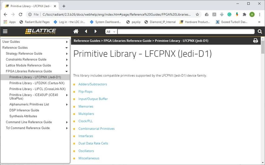
Please refer to Reference Guides > FPGA Libraries Reference Guide > Primitive Library - of the Lattice
Radiant Software Help for more information on these FPGA primitives. Figure 2.3 navigates the LFCPNX Primitive
Library from the Lattice Radiant Software Help.
Figure 2.3. Reference Guide for the Primitive Library
© 2020-2021 Lattice Semiconductor Corp. All Lattice trademarks, registered trademarks, patents, and disclaimers are as listed at www.latticesemi.com/legal.
All other brand or product names are trademarks or registered trademarks of their respective holders. The specifications and information herein are subject to change without notice.
14 FPGA-IPUG-02154-1.1LPDDR4 Memory Interface Module - Lattice Radiant Software
User Guide
2.4.1. Input/Output DELAY
The DELAY blocks can be used to delay the signal in either of the following paths:
Delay the input signal – from the input pin to the IDDR or IREG or FPGA Fabric
Delay the output signal – from the ODDR, OREG or FPGA fabric to the output pin
This is useful to adjust for any skews amongst the input or output data bus. It can also be used to generate skew
between the bits of output bus to reduce SSO noise. The DELAY block can be used with IDDR or ODDR modules, SDR
module, as well as on the direct input pin of the FPGA. The DELAY is shared by the input and output paths and hence
can only be used either to delay the input data or the output signal on a given pin.
The delayed value are set using:
Pre-determined delay value (for Zero Hold time, delay based on Interface Type)
Fixed delay values entered by user
Dynamically updated using counter up and down controls
The DELAY block can be completely bypassed as well.
2.4.1.1. DELAYA
By default, the DELAYA primitive is configured to factory delay settings based on the clocking structure. Users can
update the DELAY setting using the MOVE and DIRECTION control inputs. The LOAD_N resets the delay back to the
default value.
DELAYA
A Z
LOAD_N
EDETERR
MOVE
DIRECTION CFLAG
COARSE0
COARSE1
Figure 2.4. DELAYA Block Diagram
2.4.1.2. DELAYB
The DELAYB primitive is be configured to factory delay settings based on the clocking structure. Users cannot change
the delay when using this module.
DELAYB
A Z
Figure 2.5. DELAYB Block Diagram
2.4.1.3. OUTDELAYA
The OUTDELAYA primitive is used to add static and dynamic delay to DOUT and TOUT for write training in LPDDR4
mode.
© 2020-2021 Lattice Semiconductor Corp. All Lattice trademarks, registered trademarks, patents, and disclaimers are as listed at www.latticesemi.com/legal.
All other brand or product names are trademarks or registered trademarks of their respective holders. The specifications and information herein are subject to change without notice.
FPGA-IPUG-02154-1.1 15LPDDR4 Memory Interface Module - Lattice Radiant Software
User Guide
OUTDELAYA
DOUTI
TOUTI DOUT
LOAD_N_LPDDR4_WT TOUT
MOVE_LPDDR4_WT COUT_LPDDR4_WT
DIRECTION_LPDDR4_WT
Figure 2.6. OUTDELAYA Block Diagram
2.4.2. IDDR/ODDR
This section describes the primitives used to build LPDDR2, DDR3 and LPDDR4 memory interfaces. Some of these
primitives are also used to generate generic DDR functions that use DQS clocking tree. The IDDR/ODDR primitives
support 4:1(X2), 8:1(X4), gearing modes that are used to implement the memory functions. The gearing mode defines
the ratio of system clock and DDR clock frequencies. The data from the FPGA fabric transferred using the rising edge of
system clock (slower frequency) while the data in DDR interface side is transferred in both edges of the DDR clock
(faster frequency).
A 4:1 (X2) gearing mode means:
Clock frequency ratio: 1 system clock : 2 DDR clock
Data bit width ratio: 4 bits of data in system clock rising edge: 1 bit of data in for each of 4 DDR clock edges
Similarly, an 8:1 (X4) gearing mode means:
Clock frequency ratio: 1 system clock : 8 DDR clock
Data bit width ratio: 8 bits of data in system clock rising edge: 1 bit of data in for each of 8 DDR clock edges
Thus, it is recommended to use X4 gearing mode when a low system clock frequency or a high DDR clock frequency is
desired.
2.4.2.1. IDDRX4DQ
This primitive is used to capture the data bits from DDR3 or LPDDR4 interface for X4 gearing mode.
D IDDRX4DQ Q0
DQSR90 Q1
Q2
ECLK
Q3
SCLK
Q4
RST
Q5
RDPNTR[2:0] Q6
WRPNTR[2:0] Q7
Figure 2.7. IDDRX2DQ Block Diagram
© 2020-2021 Lattice Semiconductor Corp. All Lattice trademarks, registered trademarks, patents, and disclaimers are as listed at www.latticesemi.com/legal.
All other brand or product names are trademarks or registered trademarks of their respective holders. The specifications and information herein are subject to change without notice.
16 FPGA-IPUG-02154-1.1LPDDR4 Memory Interface Module - Lattice Radiant Software
User Guide
2.4.2.2. ODDRX4DQ
This primitive is used to generate the DQ data output of DDR3 or LPDDR4 memory interface for X4 gearing mode.
D0 ODDRX4DQ
D1
D2
D3
D4 Q
D5
D6
D7
DQSW270
ECLK
SCLK
RST
Figure 2.8. ODDRX4DQ Block Diagram
2.4.3. ODDRX4DQS
This primitive is used to generate DQS clock output of DDR3 and LPDDR4 memory for X4 gearing.
D0 ODDRX4DQS
D1
D2
D3
D4 Q
D5
D6
D7
DQSW
ECLK
SCLK
RST
Figure 2.9. ODDRX4DQS Block Diagram
2.4.4. Memory Output DDR Primitives for Tristate Output Control
The following are the primitives used to implement tristate control for the outputs to the DDR memory.
2.4.4.1. TSHX4DQ
This primitive is used to generate the tristate control for DQ data output of DDR3 memory interface with x4 gearing
mode.
TSHX4DQ
T0
T1
T2
Q
T3
DQSW270
ECLK
SCLK
RST
Figure 2.10. TSHX4DQ Block Diagram
© 2020-2021 Lattice Semiconductor Corp. All Lattice trademarks, registered trademarks, patents, and disclaimers are as listed at www.latticesemi.com/legal.
All other brand or product names are trademarks or registered trademarks of their respective holders. The specifications and information herein are subject to change without notice.
FPGA-IPUG-02154-1.1 17LPDDR4 Memory Interface Module - Lattice Radiant Software
User Guide
2.4.4.2. TSHX4DQS
This primitive is used to generate the tristate control to DQS output for DDR3 or LPDDR4 memory interface for x4
gearing mode.
TSHX4DQS
T0
T1
T2
Q
T3
DQSW
ECLK
SCLK
RST
Figure 2.11. TSHX4DQS Block Diagram
2.4.5. OSHX4
This primitive is used to generate the address and command signals of DDR3 or LPDDR4 memory interface for x4
gearing mode and write leveling.
D0 OSHX4
D1
D2
D3 Q
ECLK
SCLK
RST
Figure 2.12. OSHX4 Block Diagram
2.4.6. DDRDLL
DDRDLL generates a phase shift code (90 degree) according to its running frequency. This code is provided to every
individual DQS block and DLLDEL slave delay element located in 2 adjacent sides if available.
DDRDLL
FREEZE CODE[8:0]
CLKIN LOCK
RST DCNTL[8:0]
UDDCNTL_N
Figure 2.13. DDRDLL Block Diagram
© 2020-2021 Lattice Semiconductor Corp. All Lattice trademarks, registered trademarks, patents, and disclaimers are as listed at www.latticesemi.com/legal.
All other brand or product names are trademarks or registered trademarks of their respective holders. The specifications and information herein are subject to change without notice.
18 FPGA-IPUG-02154-1.1LPDDR4 Memory Interface Module - Lattice Radiant Software
User Guide
2.4.7. ECLKDIV
ECLKDIV
DIVRST
ECLKIN DIVOUT
SLIP
TESTINP[3:0]
Figure 2.14. ECLKDIV Block Diagram
2.4.8. ECLKSYNC
ECLKSYNC
ECLKIN ECLKOUT
STOP
Figure 2.15. ECLKSYNC Block Diagram
2.4.9. DQSBUF_IVREF
To support DDR memory interfaces (DDR2/3, LPDDR2/3/4), the DQS strobe signal from the memory must be used to
capture the data (DQ) in the PIC registers during memory reads.
DQSBUF_IVREF
DQSI BTDETECT
PAUSE BURSTDETECT
RDCLKSEL[3:0] DATAVALID
RDDIR DQSW
RDLOADN DQSWRD
READ[3:0] RDPNTR[2:0]
READMOVE READCOUT
RST DQSR90
SCLK DQSW270
SELCLK WRCOUT
WRDIR WRLVCOUT
WRLOAD_N WRPNTR[2:0]
WRLVDIR
WRLVLOAD_N
WRLVMOVE
WRMOVE
ECLKIN
RSTSMCNT
DLLCODE[8:0]
IVREFI[6:0]
Figure 2.16. DQSBUF_IVREF Block Diagram
© 2020-2021 Lattice Semiconductor Corp. All Lattice trademarks, registered trademarks, patents, and disclaimers are as listed at www.latticesemi.com/legal.
All other brand or product names are trademarks or registered trademarks of their respective holders. The specifications and information herein are subject to change without notice.
FPGA-IPUG-02154-1.1 19LPDDR4 Memory Interface Module - Lattice Radiant Software
User Guide
2.5. Clock Synchronization Logic
Figure 2.17 shows the block diagram of the clock synchronization logic. The PLL generates the following clocks:
CLKOP – a slow clock equal to the frequency of the reference lock – set by PLL Input Frequency attribute.
This clock is used to clock the MEM_SYNC.
CLKOS – used for sclk_o and eclk_o (internal DDR clock that clocks the DDR primitives) generation.
The CLKOS frequency is set by DDR Memory Frequency attribute, which is the operating clock. The CLKOS
frequency is selectable between operating clock (DDR Memory Frequency) and 50 MHz which is the command bus
training clock.
The ECLKSYNC and ECLKDIV generates the eclk_o and sclk_o respectively. These clocks are routed to a dedicated clock
route resource which ensures correct timing. The DDRDLL generates the DLL code which is used by the DQSBUF for
generating the correct phase delays of the internal clocks for the data path. These DDR clock primitives are controlled
by MEM_SYNC which is implemented in soft logic.
PLL ECLKSYNC ECLKDIV
pll_refclk_i sclk_o
REFCLK ECLKOUT ECLKIN DIVOUT
1'b0 SLIP
CLKOS ECLKIN STOP
4'h0 TERSTINP[3:0]
LOCK
LMMI I/F DIVRST
eclk_o
MEM_SYNC
LMMI I/F DDRDLL
DLL_LOCK STOP CLKIN LOCK
pll_lock_o DDR_RESET dllcode[8:0]
PLL_LOCK CODE[8:0]
DLL_RESET RST
sync_clk_i
SYNC_CLK UDDCNTLN UDDCNTL_N
FREEZE FREEZE
clk_sel_i
CLK_SEL ready_o
READY
clk_update_i
CLK_UPDATE ddr_rst_o
DDR_RST
rst_i
RST
PAUSE pause_o
pause_i
Figure 2.17. Clock Synchronization Logic Block Diagram
An example of clock frequency change timing diagram is shown in Figure 2.18, the order of signal transitions are
accurate but the cycle by cycle relationship is not. This is because the signals are operating in 3 clock – sclk_o, internal
eclk_o (CLKOS) and CLKOP (not shown). The signals moving across clock domains avoid metastability by implementing
clock crossing logic or only allow transition during freeze/stop/pause signals are asserted.
The clock frequency change is initiated by a Low to High transition on clk_update_i signal and the ddr_clk_sel_i
specifies the target new frequency: 1’b0 for Operating Frequency and 1’b1 for command bus training frequency. The
ready_o signal negates in the next sclk_o cycle, indicating that the sclk_o and ddr_ck_o are not yet ready. The
controller must not issue any request - command/data/delay code update while ready_o signal is low. The
MEM_SYNC.freeze signal asserts and is followed by MEM_SYNC.stop assertion to properly stop the sclk_o and eclk_o
before the actual PLL clock change which occurs during both freeze and stop signals asserted. When these signals are
negated, the PLL is already generating the target frequency. The sclk_o and ddr_ck_o resumes at the target
frequencies.
© 2020-2021 Lattice Semiconductor Corp. All Lattice trademarks, registered trademarks, patents, and disclaimers are as listed at www.latticesemi.com/legal.
All other brand or product names are trademarks or registered trademarks of their respective holders. The specifications and information herein are subject to change without notice.
20 FPGA-IPUG-02154-1.1LPDDR4 Memory Interface Module - Lattice Radiant Software
User Guide
Figure 2.18. Clock Synchronization Logic Block Diagram
The DLL code need to be updated for the new frequency. This is done by asserting the MEM_SYNC.dll_reset, the pause
signal is asserted before and after dll_reset to avoid metastability. The DDRDLL.lock negates after the dll_reset and
asserts after the DDRDLL locks to the new frequency. The MEM_SYNC.uddcntln pulses to update the DLL code, the
pause_o is also asserted before and after this pulse for the DQSBUF to properly update for the new DLL code.
The ready_o signal asserts to indicate that the clocks are now stable and the module is now ready to receive new
requests from the controller. The clk_update_i may be negated any time after the ready_o signal asserts.
2.6. Data Input/Output Path
The block diagram of Data Input/Output Path describing the DDR primitives connections are shown in Figure 2.19.
© 2020-2021 Lattice Semiconductor Corp. All Lattice trademarks, registered trademarks, patents, and disclaimers are as listed at www.latticesemi.com/legal.
All other brand or product names are trademarks or registered trademarks of their respective holders. The specifications and information herein are subject to change without notice.
FPGA-IPUG-02154-1.1 21LPDDR4 Memory Interface Module - Lattice Radiant Software
User Guide
dqs_i[DW/2-1:0]
dqs_oe_n_i[DW-1:0]
ODDRX4DQS
DQSBUF_IVREF [j] D0
Q
ddr_dqs_io
[DW/8+j] D1
burst_det_o[DW/8-1:0] BTDETECT DQSI [2*DW/8+j] D2 [DW/8-1:0]
[3*DW/8+j] (differential pair)
burst_det_sclk_o[DW/8-1:0] BURSTDETECT
D3
data_valid_o[DW/8-1:0] TSHX4DQS [4*DW/8+j] D4
DATAVALID [j] T0 [5*DW/8+j] D5
Q [6*DW/8+j] D6
rd_section_o[DW/8-1:0] DQSWRD
[DW/8+j] T1
[7*DW/8+j] D7
[2*DW/8+j] T2
DQSW
[3*DW/8+j] T3
rd_i[3:0] READ[3:0] ECLK
DQSW DQSW
rd_clksel_i[3:0] RDCLKSEL[3:0] ECLK SCLK
SCLK RST
selclk_i SELCLK RST
rd_load_n_i[DW/8-1:0] RDLOAD_N OUTDELAYA
rd_move_i[DW/8-1:0] READMOVE DOUTI DOUT
rd_dir_i[DW/8-1:0] RDDIR
TOUTI TOUT
Per. Bit Delay Adj. Signals
rd_cout_o[DW/8-1:0] READCOUT
wrlvl_load_n_i[DW/8-1:0] IDDRX4DQ DELAYA
WRLVLOAD_N D Q0 [i] Z A
wrlvl_move_i[DW/8-1:0] WRLVMOVE DQSR90 DQSR90 Q1
wrlvl_dir_i[DW/8-1:0] RDPNTR[2:0] RDPNTR[2:0]
Q2 [2*DW+i] Per. Bit Delay Adj. Signals ddr_dq_io
WRLVDIR Q3
wrlvl_cout_o[DW/8-1:0] WRPNTR[2:0] WRPNTR[2:0] Q4
[DW-1:0]
WRLVCOUT
ECLK Q5 [5*DW+i] ODDRX4DQ
wr_load_n_i[DW/8-1:0] WRLOAD_N SCLK
Q6
Q7
[6*DW+i]
[7*DW+i] [i] D0
[DW+i] Q
wr_move_i[DW/8-1:0] WRMOVE RST
D1
[2*DW+i] D2
wr_dir_i[DW/8-1:0] WRDIR DQSW270 [3*DW+i] D3
[4*DW+i] D4
wr_cout_o[DW/8-1:0] WRCOUT [5*DW+i] D5
[6*DW+i] D6
dqs_grp_vref_i IDDRX4DQ [7*DW+i] D7
IVREF D Q0 [j] DQSW270
DQSR90 Q1 [DW/8+j]
pause_i (from Clock Sync Logic) PAUSE Q2 [2*DW/8+j] ECLK
RDPNTR[2:0] SCLK
sync_rst_i Q3 [3*DW/8+j]
RSTSMCNT WRPNTR[2:0] Q4 [4*DW/8+j] RST
dllcode[8:0] (from Clock Sync Logic) DLLCODE[8:0] ECLK Q5 [5*DW/8+j]
eclk_i (from Clock Sync Logic) to ECLK Q6 [6*DW/8+j]
ECLKIN SCLK Q7 [7*DW/8+j]
sclk_i (from Clock Sync Logic) to SCLK OUTDELAYA
SCLK RST TOUTI TOUT
ddr_rst_i (from Clock Sync Logic) to RST
RST
DOUTI DOUT
Per. Bit Delay Adj. Signals
dqwl_o[DW-1:0]
dmi_o[DW-1:0] OUTDELAYA
TOUTI TOUT
DOUTI DOUT
dq_o[8*DW-1:0] Per. Bit Delay Adj Signals
dq_i[8*DW-1:0]
DELAYA
Z A
ddr_dmi_io
Per Bit Delay Adj. [DW/8-1:0]
Per. Bit Delay Adj. Signals
TSHX4DQ
[j] T0
Q
ODDRX4DQ
[DW/8+j] T1 [j] D0
[2*DW/8+j] T2 [DW/8+j] D1 Q
[3*DW/8+j] T3 [2*DW/8+j] D2
DQSW270 [3*DW/8+j] D3
ECLK [4*DW/8+j] D4
dq_outen_n_i[DW/2-1:0] SCLK [5*DW/8+j] D5
RST [6*DW/8+j] D6
[7*DW/8+j] D7
DQSW270
ECLK
dmi_i[DW-1:0] SCLK
RST
Figure 2.19. Data Input/Output Path Block Diagram
The DQSBUF_IVREF generates the following 3 internal clocks which are generated according to the DLL code:
DQSW – clocks the write DQS. The delay is controlled by the wrlvl_ signals (write leveling).
DQSW270 – clocks the write DQ/DMI. The delay is controlled by the wr_ signals
DQSR90 – clocks the read DQ/DMI. The delay is controlled by the rd_ signals
This internal clock is only activated when a read pre-amble DQS=0 followed by DQS pulse has been successfully
captured. A read BL16 produces eight DQSR90 pulses.
Important Note:
The delay codes of DQSBUF_IVREF is not initialized during reset. The controller or user logic must reset the delay codes
by driving 0 logic to wrlvl_load_n, wr_load_n and rd_load_n before performing any training.
© 2020-2021 Lattice Semiconductor Corp. All Lattice trademarks, registered trademarks, patents, and disclaimers are as listed at www.latticesemi.com/legal.
All other brand or product names are trademarks or registered trademarks of their respective holders. The specifications and information herein are subject to change without notice.
22 FPGA-IPUG-02154-1.1LPDDR4 Memory Interface Module - Lattice Radiant Software
User Guide
2.6.1. Write Data access
Figure 2.20 shows the timing diagram example for write BL16 data access with Data Bus Width = 32 (DQS group = 4).
The pre-amble is 2nCK cycles and the post amble for this example is 0.5nCK. The 2nCK pre-amble is generated by
setting write_dqs_i =0xFF. F during disable cycle and enabling DQS 1 CK earlier than the DQ/DMI. The input is internally
registered at the first rising edge of sclk_o and is outputted serially after 2 sclk_o cycles. Thus, the latency is 3 sclk_o
cycles. The output enable signal write_dqs_oe_n_i and write_dq_oe_n_i are 4x the bit with of the DQS group (DW/8).
The first DW/8 bits controls the output enable for the DDR clock cycle that crosses the sclk_o rising edge. The least
significant bytes/bits of write_dq_i/write_dmi_i are transmitted first in the DDR side. In the diagram, the lower bits of
write_dq_i/write_dmi_i are don’t care because the corresponding write_dq_oe_n_i bits are “1” (output disabled).
Adding 1 ddr_ck_o cycle latency in DDR side means shifting the inputs in the User Interface side. For example the
Figure 2.21 is equal to Figure 2.20 with added 2nCK latency.
Figure 2.20. Write BL16 timing diagram
Figure 2.21. Write BL16 timing diagram with added 2nCK latency
2.6.2. Read Data access
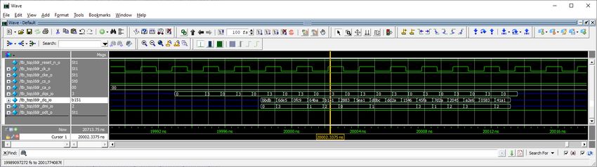
The read_dqs_ie_i signals the DQSBUF to capture the incoming read burst, the bits[3:0] indicates that corresponding
DDR clock cycle is captured. In Figure 2.22, read_dqs_ie_i = 4’hF for 2 consecutive SCLK cycles, starting from sclk_o
rising edge at tick 9. This means the 8x2=16 samples of DQ/DMI are captured continuously starting from next rising
edge of internal DDR clock for read path after the sclk_o rising edge at tick 25 – this is 3 SCLK rising edge including the
1st , read_dqs_ie_i = 4’hF sample. The pre-amble with a DQS pulse must be provided before this time.
Figure 2.22. Read BL16 timing diagram (rd_clksel_i =4’h0)
When the read preamble and eight DQS pulses are captured properly, burst_det_sclk_o asserts for two sclk_o cycles or
more. If burst_det_sclk_o did not assert or has asserted for only 1 sclk_o cycle, that means the captured read DQ/DMI
is unreliable. The timing of assertion of burst_det_sclk_o depends on asynchronous (with respect to sclk_o) reception
of the incoming burst. Thus, actual assertion time is difficult to predict. Because of this, this signal is only used during
DQS Read Training and Read Training.
© 2020-2021 Lattice Semiconductor Corp. All Lattice trademarks, registered trademarks, patents, and disclaimers are as listed at www.latticesemi.com/legal.
All other brand or product names are trademarks or registered trademarks of their respective holders. The specifications and information herein are subject to change without notice.
FPGA-IPUG-02154-1.1 23You can also read