Target Board Kit S5D3 (TB-S5D3) - Mouser Electronics
←
→
Page content transcription
If your browser does not render page correctly, please read the page content below
User’s Manual

                Target Board Kit S5D3 (TB-S5D3)
                                                                                            User’s Manual

                Renesas Synergy™ Platform
                Synergy Tools & Kits
                Kits: TB-S5D3 v1.0

                 All information contained in these materials, including products and product specifications, represents
                 information on the product at the time of publication and is subject to change by Renesas Electronics
                 Corp. without notice. Please review the latest information published by Renesas Electronics Corp.
                 through various means, including the Renesas Electronics Corp. website (http://www.renesas.com).

                www.renesas.com                                                         Rev.1.01 Feb 2019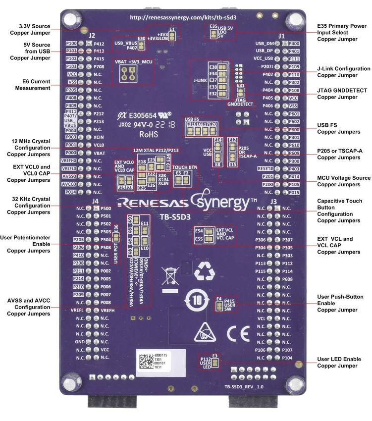
Notice
1.  Descriptions of circuits, software and other related information in this document are provided only to illustrate the operation of semiconductor products
    and application examples. You are fully responsible for the incorporation or any other use of the circuits, software, and information in the design of your
    product or system. Renesas Electronics disclaims any and all liability for any losses and damages incurred by you or third parties arising from the use
    of these circuits, software, or information.
2. Renesas Electronics hereby expressly disclaims any warranties against and liability for infringement or any other claims involving patents, copyrights,
    or other intellectual property rights of third parties, by or arising from the use of Renesas Electronics products or technical information described in this
    document, including but not limited to, the product data, drawings, charts, programs, algorithms, and application examples.
3. No license, express, implied or otherwise, is granted hereby under any patents, copyrights or other intellectual property rights of Renesas Electronics
    or others.
4. You shall not alter, modify, copy, or reverse engineer any Renesas Electronics product, whether in whole or in part. Renesas Electronics disclaims any
    and all liability for any losses or damages incurred by you or third parties arising from such alteration, modification, copying or reverse engineering.
5. Renesas Electronics products are classified according to the following two quality grades: “Standard” and “High Quality”. The intended applications for
    each Renesas Electronics product depends on the product’s quality grade, as indicated below.
        "Standard": Computers; office equipment; communications equipment; test and measurement equipment; audio and visual equipment; home
                       electronic appliances; machine tools; personal electronic equipment; industrial robots; etc.
        "High Quality": Transportation equipment (automobiles, trains, ships, etc.); traffic control (traffic lights); large-scale communication equipment; key
                          financial terminal systems; safety control equipment; etc.
    Unless expressly designated as a high reliability product or a product for harsh environments in a Renesas Electronics data sheet or other Renesas
    Electronics document, Renesas Electronics products are not intended or authorized for use in products or systems that may pose a direct threat to
    human life or bodily injury (artificial life support devices or systems; surgical implantations; etc.), or may cause serious property damage (space
    system; undersea repeaters; nuclear power control systems; aircraft control systems; key plant systems; military equipment; etc.). Renesas Electronics
    disclaims any and all liability for any damages or losses incurred by you or any third parties arising from the use of any Renesas Electronics product
    that is inconsistent with any Renesas Electronics data sheet, user’s manual or other Renesas Electronics document.
6. When using Renesas Electronics products, refer to the latest product information (data sheets, user’s manuals, application notes, “General Notes for
    Handling and Using Semiconductor Devices” in the reliability handbook, etc.), and ensure that usage conditions are within the ranges specified by
    Renesas Electronics with respect to maximum ratings, operating power supply voltage range, heat dissipation characteristics, installation, etc.
    Renesas Electronics disclaims any and all liability for any malfunctions, failure or accident arising out of the use of Renesas Electronics products
    outside of such specified ranges.
7. Although Renesas Electronics endeavors to improve the quality and reliability of Renesas Electronics products, semiconductor products have specific
    characteristics, such as the occurrence of failure at a certain rate and malfunctions under certain use conditions. Unless designated as a high reliability
    product or a product for harsh environments in a Renesas Electronics data sheet or other Renesas Electronics document, Renesas Electronics
    products are not subject to radiation resistance design. You are responsible for implementing safety measures to guard against the possibility of bodily
    injury, injury or damage caused by fire, and/or danger to the public in the event of a failure or malfunction of Renesas Electronics products, such as
    safety design for hardware and software, including but not limited to redundancy, fire control and malfunction prevention, appropriate treatment for
    aging degradation or any other appropriate measures. Because the evaluation of microcomputer software alone is very difficult and impractical, you
    are responsible for evaluating the safety of the final products or systems manufactured by you.
8. Please contact a Renesas Electronics sales office for details as to environmental matters such as the environmental compatibility of each Renesas
    Electronics product. You are responsible for carefully and sufficiently investigating applicable laws and regulations that regulate the inclusion or use of
    controlled substances, including without limitation, the EU RoHS Directive, and using Renesas Electronics products in compliance with all these
    applicable laws and regulations. Renesas Electronics disclaims any and all liability for damages or losses occurring as a result of your noncompliance
    with applicable laws and regulations.
9. Renesas Electronics products and technologies shall not be used for or incorporated into any products or systems whose manufacture, use, or sale is
    prohibited under any applicable domestic or foreign laws or regulations. You shall comply with any applicable export control laws and regulations
    promulgated and administered by the governments of any countries asserting jurisdiction over the parties or transactions.
10. It is the responsibility of the buyer or distributor of Renesas Electronics products, or any other party who distributes, disposes of, or otherwise sells or
    transfers the product to a third party, to notify such third party in advance of the contents and conditions set forth in this document.
11. This document shall not be reprinted, reproduced or duplicated in any form, in whole or in part, without prior written consent of Renesas Electronics.
12. Please contact a Renesas Electronics sales office if you have any questions regarding the information contained in this document or Renesas
    Electronics products.
(Note1)   “Renesas Electronics” as used in this document means Renesas Electronics Corporation and also includes its directly or indirectly controlled
          subsidiaries.
(Note2)   “Renesas Electronics product(s)” means any product developed or manufactured by or for Renesas Electronics.

                                                                                                                                   (Rev.4.0-1 November 2017)

 Corporate Headquarters                                                                 Contact information
 TOYOSU FORESIA, 3-2-24 Toyosu,                                                         For further information on a product, technology, the most up-to-date
 Koto-ku, Tokyo 135-0061, Japan                                                         version of a document, or your nearest sales office, please visit:
 www.renesas.com                                                                        www.renesas.com/contact/.

 Trademarks
 Renesas and the Renesas logo are trademarks of Renesas Electronics
 Corporation. All trademarks and registered trademarks are the property
 of their respective owners.

                                                                                                 © 2019 Renesas Electronics Corporation. All rights reserved.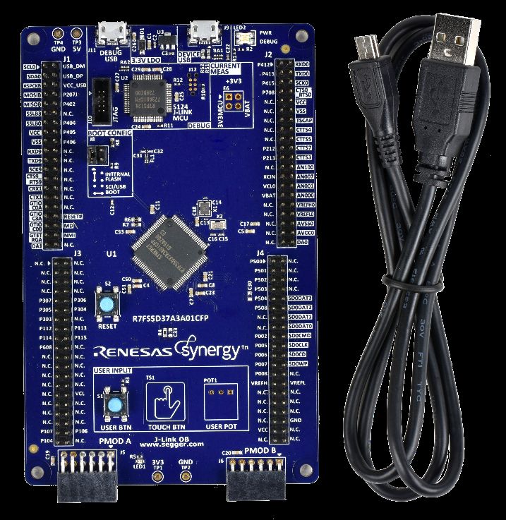
Renesas Synergy™ Target Board Kit S5D3 (TB-S5D3) Disclaimer
By using this TB-S5D3, the user accepts the following terms, which are in addition to, and control in the event of disagreement, with Renesas’ General
Terms and Conditions available at https://www.renesas.com/en-us/legal/disclaimer.html.
The TB-S5D3 is not guaranteed to be error free, and the entire risk as to the results and performance of the TB-S5D3 is assumed by the User. The TB-
S5D3 is provided by Renesas on an “as is” basis without warranty of any kind whether express or implied, including but not limited to the implied warranties
of satisfactory quality, fitness for a particular purpose, title, and non-infringement of intellectual property rights with regard to the TB-S5D3. Renesas
expressly disclaims all such warranties.
Renesas does not consider the TB-S5D3 a finished product and therefore the TB-S5D3 may not yet comply with some requirements applicable to finished
products, including, but not limited to recycling (WEEE), CE, UL, restricted substances (ROHS), FCC, FEE, and electromagnetic compatibility regulations.
Renesas or its affiliates shall in no event be liable for any loss of profit, loss of data, loss of contract, loss of business, damage to reputation or goodwill, any
economic loss, any reprogramming or recall costs (whether the foregoing losses are direct or indirect) nor shall Renesas or its affiliates be liable for any
other direct or indirect special, incidental or consequential damages arising out of or in relation to the use of this TB-S5D3, even if Renesas or its affiliates
have been advised of the possibility of such damages.
Renesas has used reasonable care in preparing the information included in this document, but Renesas does not warrant that such information is error free
nor does Renesas guarantee an exact match for every application or parameter to part numbers designated by other vendors listed herein. The information
provided in this document is intended solely to enable the use of Renesas products. No express or implied license to any intellectual property right is
granted by this document or in connection with the sale of Renesas products. Renesas reserves the right to make changes to specifications and product
descriptions at any time without notice. Renesas assumes no liability for any damages incurred by you resulting from errors in or omissions from the
information included herein. Renesas cannot verify, and assumes no liability for, the accuracy of information available on another company’s website.

Precautions
This Renesas Synergy™ Target Board Kit is only intended for use in a laboratory environment under ambient temperature and humidity conditions. A safe
separation distance should be used between this and any sensitive equipment. Its use outside the laboratory, classroom, study area, or similar such area
invalidates conformity with the protection requirements of the Electromagnetic Compatibility Directive and could lead to prosecution.
The product generates, uses, and can radiate radio frequency energy and may cause harmful interference to radio communications. There is no guarantee
that interference will not occur in a particular installation. If this equipment causes harmful interference to radio or television reception, which can be
determined by turning the equipment off or on, you are encouraged to try to correct the interference by one or more of the following measures:
• Ensure attached cables do not lie across the equipment.
• Reorient the receiving antenna.
• Increase the distance between the equipment and the receiver.
• Connect the equipment into an outlet on a circuit different from that which the receiver is connected.
• Power down the equipment when not in use.
• Consult the dealer or an experienced radio/TV technician for help.
Note: It is recommended that wherever possible shielded interface cables are used.
The product is potentially susceptible to certain EMC phenomena. To mitigate against them it is recommended that the following measures be undertaken:
• The user is advised that mobile phones should not be used within 10 m of the product when in use.
• The user is advised to take ESD precautions when handling the equipment.
The Renesas Synergy™ Target Board Kit does not represent an ideal reference design for an end product and does not fulfill the regulatory standards for
an end product.
User’s Manual

Renesas Synergy™ Platform
Target Board Kit S5D3 (TB-S5D3)
Contents

1.      Overview .................................................................................................................................3

2.      Kit Contents .............................................................................................................................6

3.      Getting Started with Embedded Application Development on TB-S5D3 ................................... 6

4.      TB-S5D3 Hardware Details...................................................................................................... 7
4.1      Jumpers and DIP Switch Settings ........................................................................................................... 7
4.1.1      Copper Jumpers .................................................................................................................................... 7
4.1.2      Default Board Configuration .................................................................................................................. 8

5.      Hardware Layout .....................................................................................................................9
5.1      System Block Diagram ............................................................................................................................ 9
5.2      Power Requirements ............................................................................................................................. 10
5.2.1      Power Supply Options ......................................................................................................................... 10
5.2.2      Powering up the Board ........................................................................................................................ 12
5.2.3      Battery Supply Configuration............................................................................................................... 12
5.2.4      Measuring Current Consumption ........................................................................................................ 12
5.3      Main Components ................................................................................................................................. 14
5.4      Connectivity and Settings ...................................................................................................................... 15
5.4.1      Device USB ......................................................................................................................................... 15
5.4.2      Debug USB.......................................................................................................................................... 15
5.4.3      JTAG/SWD .......................................................................................................................................... 16
5.4.4      LEDs .................................................................................................................................................... 17
5.4.5      Switches .............................................................................................................................................. 17
5.4.6      PMOD A .............................................................................................................................................. 19
5.4.7      PMOD B .............................................................................................................................................. 19
5.4.8      User Capacitive Touch Button............................................................................................................. 19
5.5      Target Board Pin Headers ..................................................................................................................... 21
5.5.1      Pin Header J1 ...................................................................................................................................... 23
5.5.2      Pin Header J2 ...................................................................................................................................... 24
5.5.3      Pin Header J3 ...................................................................................................................................... 25
5.5.4      Pin Header J4 ...................................................................................................................................... 26
5.6      Additional Features................................................................................................................................ 27
5.6.1      Reference Voltages VREF and VREF0 .............................................................................................. 27
5.6.2      Analog Voltage AVCC0/AVSS0 .......................................................................................................... 27
5.6.3      On-Board Clock Crystals ..................................................................................................................... 27

R12UM0032EU0101 Rev.1.01                                                                                                                           Page 1 of 38
Feb.08.19
Renesas Synergy™ Platform                                                                          Target Board Kit S5D3 (TB-S5D3)
5.6.4      User Potentiometer ............................................................................................................................. 28
5.6.5      Boot Configuration ............................................................................................................................... 29
5.6.6      Miscellaneous Signals ......................................................................................................................... 29

6.        Electrical Schematics.......................................................................................................... 31

7.      Mechanical Drawing .............................................................................................................. 35

8.      Certifications .......................................................................................................................... 36

Revision History ............................................................................................................................ 38

R12UM0032EU0101 Rev.1.01                                                                                                                     Page 2 of 38
Feb.08.19
Renesas Synergy™ Platform Target Board Kit S5D3 (TB-S5D3)
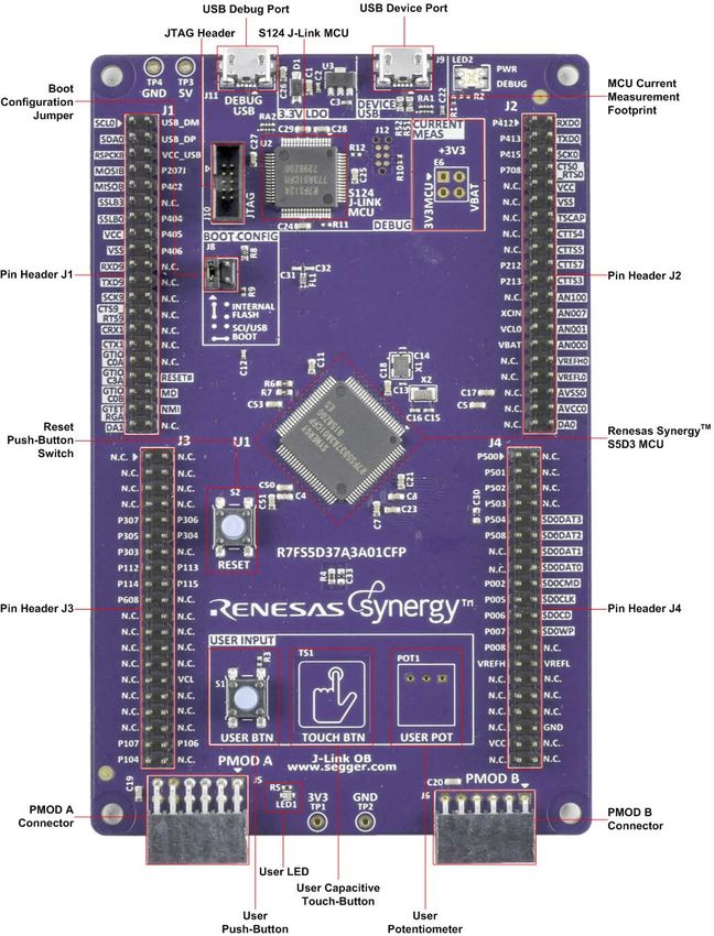
1. Overview
The Target Board Kit S5D3 (TB-S5D3) enables developers to get started with initial firmware development
and evaluate the Synergy Software Package (SSP) on the S5D3 MCU Group.
• Renesas Synergy™ S5D3 Microcontroller Group
R7FS5D37A3A01CFP
100-pin LQFP package
120 MHz Arm® Cortex®-M4 core with Floating Point Unit (FPU)
256 KB SRAM
512 KB code flash memory
8 KB data flash memory
• Connectivity
A Device USB connector for the Main MCU
S124 MCU-based SEGGER J-Link® On-board (OB) interface for debugging and programming of the
S5D3 MCU. A 10-pin JTAG/SWD interface is also provided for connecting optional external debuggers
and programmers.
Two PMOD connectors, allowing use of appropriate PMOD compliant peripheral plug-in modules for
rapid prototyping
Pin headers for access to power and signals for the Main MCU
• Multiple clock sources
Main MCU oscillator crystals, providing precision 12.000 MHz and 32,768 Hz reference clocks
Additional low-precision clocks are available internal to the Main MCU
• MCU reset push-button switch
• MCU boot configuration jumper
• General purpose I/O ports
One jumper to allow measuring of Main MCU current
Copper jumpers on PCB bottom side for configuration and access to selected MCU signals
• Operating voltage
External 5 V input through the Debug USB connector supplies the on-board power regulator to power
the Target Board logic and interfaces. External 5 V or 3.3 V may be also supplied through alternate
locations on the Target Board.
• A two-color board status LED indicating availability of regulated power and connection status of the J-Link
interface
• A red User LED, controlled by the Main MCU firmware
• A User Push-Button switch, User Capacitive Touch Button sensor, and an optional User Potentiometer,
all of which are controlled by the Main MCU firmware
R12UM0032EU0101 Rev.1.01 Page 3 of 38
Feb.08.19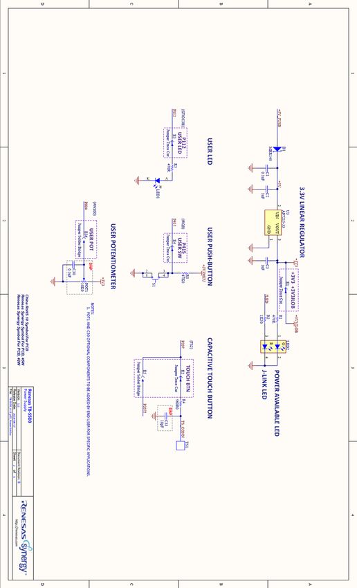
Renesas Synergy™ Platform                           Target Board Kit S5D3 (TB-S5D3)

                            Figure 1. TB-S5D3 Top Side

R12UM0032EU0101 Rev.1.01                                                 Page 4 of 38
Feb.08.19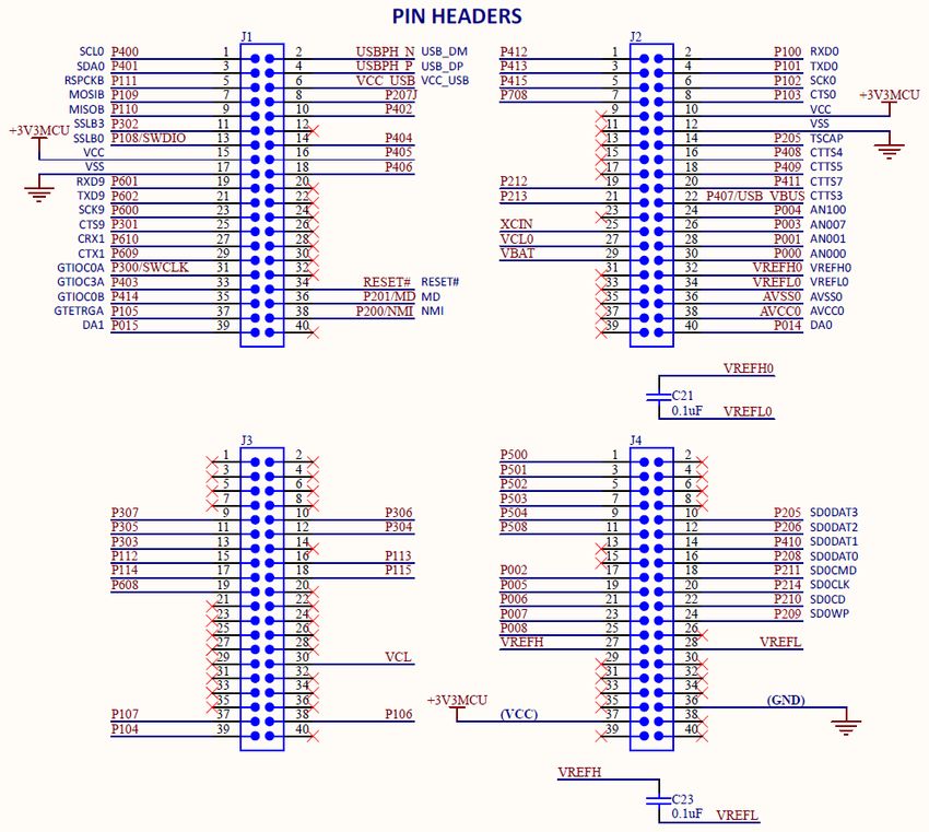
Renesas Synergy™ Platform                            Target Board Kit S5D3 (TB-S5D3)

                            Figure 2. TB-S5D3 Bottom Side

R12UM0032EU0101 Rev.1.01                                                  Page 5 of 38
Feb.08.19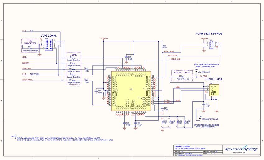
Renesas Synergy™ Platform                                       Target Board Kit S5D3 (TB-S5D3)
2. Kit Contents
The following components are included in the Target Board Kit S5D3 (TB-S5D3):
• 1x TB-S5D3 board
• 1x USB Type-A to USB Micro-B cable

                                     Figure 3. TB-S5D3 Contents
3.   Getting Started with Embedded Application Development on TB-S5D3
To develop and execute embedded applications on the TB-S5D3 using the Synergy Platform, Synergy
Software Package and development tools are required to be installed on your computer.
Step 1: Create My Renesas Account (if you do not have one already)
You need a My Renesas account to download software, development tools, and application projects. Log in
to or Sign up for a My Renesas account at www.update.renesas.com/SSO/login.

R12UM0032EU0101 Rev.1.01                                                                   Page 6 of 38
Feb.08.19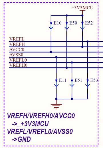
Renesas Synergy™ Platform                                            Target Board Kit S5D3 (TB-S5D3)
Step 2: Download and Install Synergy Software Package and Development Tools
The Synergy Software Package, J-Link USB drivers, and one of the two supported tool chains are bundled
and available as single downloadable file as follows:
   A. IAR Platform Installer installs Synergy Software Package and IAR Embedded Workbench® for
      Renesas Synergy™ IDE with IAR complier and J-Link USB drivers.
      Download from www.renesas.com/synergy/ewsynergy.
   B. e2 studio Platform Installer installs Synergy Software Package and e2 studio for Synergy IDE with
      IAR complier and J-Link USB drivers.
      Download from www.renesas.com/synergy/e2studio.
Note: The TB-S5D3 uses J-Link® On-board (OB) debug interface. While J-Link drivers are necessary to
       establish debug connection between the host PC and the TB-S5D3, they are not required to run the
       Out-of-Box (OoB) Demonstration (Blinky) Application that the TB-S5D3 comes pre-programmed with.
       Refer to the TB-S5D3 Quick Start Guide for more details.
Step 3: Explore Existing Application Projects for the TB-S5D3
Renesas provides several application projects to demonstrate different capabilities of the S5D3 MCU Group.
These application projects can also serve as a good starting point for you to develop your custom
applications. Application projects available for the TB-S5D3 are listed at www.renesas.com/synergy/tb-s5d3.
Notes: 1. Every application project includes the project files, an application note, and instructions to import
           the application project.
        2. On downloading the application project from the website to your computer, the application projects
           have to be built using one of the two supported tool chains before they can be downloaded on to
           the TB-S5D3 board.
4. TB-S5D3 Hardware Details
4.1     Jumpers and DIP Switch Settings
4.1.1    Copper Jumpers
Copper jumpers are of two types, designated trace-cut and solder-bridge.
A trace-cut jumper is provided with a narrow copper trace connecting its pads. The silk screen overlay
printing around a trace-cut jumper is a solid box. To isolate the pads, cut the trace between pads adjacent to
each pad, then remove the connecting copper foil either mechanically or using heat. Once the etched copper
trace is removed, the trace-cut jumper is turned into a solder-bridge jumper for any later changes.
A solder-bridge jumper is provided with two isolated pads that may be joined together by one of three
methods:
• Solder may be applied to both pads to develop a bulge on each and the bulges joined by touching a
     soldering iron across the two pads.
• A small wire may be placed across the two pads and soldered in place.
• A SMT resistor, size 0805, 0603, or 0402, may be placed across the two pads and soldered in place. A
     zero-ohm resistor shorts the pads together.
The silk screen overlay printing around a solder-bridge jumper is a box with a gap in the lines adjacent to the
isolation region between the pads.
For any copper jumper, the connection is considered closed if there is an electrical connection between the
pads (default for trace-cut jumpers.) The connection is considered open if there is no electrical connection
between the pads (default for the solder-bridge jumpers.)

                                        Figure 4. Copper Jumpers

R12UM0032EU0101 Rev.1.01                                                                          Page 7 of 38
Feb.08.19
Renesas Synergy™ Platform Target Board Kit S5D3 (TB-S5D3)
4.1.2 Default Board Configuration
The following table describes the default settings for each jumper on the TB-S5D3. This includes traditional
pin jumpers (Jx designation) and copper jumpers (Ex designation).
The Circuit Group for each jumper is the designation found in the board schematic. See section 6, Electrical
Schematics. Functional details for many of the listed jumpers may be found in section 5.4, Connectivity and
Settings and section 5.6, Additional Features.
Table 1. Default Jumper Settings
Location Circuit Group Default Function
Open/
Closed
J8 MCU Mode Config Shunt Sets the MCU Mode to boot from Internal Flash
on
pins 1-2
E18 12M Crystal Open Connects MCU P213 to pin header
E19 Open Connects MCU P212 to pin header
E23 Closed Connects 12.000 MHz Crystal to MCU P213
E24 Closed Connects 12.000 MHz Crystal to MCU P212
E1 3.3 V Linear Regulator Closed Alternate 3.3 V source (+3V3JLOB)
E22 32K Crystal Open Connects MCU XCIN to pin header
E25 Closed Connects 32.768 kHz Crystal to MCU XCIN
E26 Closed Connects 32.768 kHz Crystal to MCU XCOUT
E10 AVCC0/AVSS0 Closed Connects MCU AVCC0 TO +3V3MCU
E11 Closed Connects MCU AVSS0 to Ground
E2 Capacitive Touch Closed Enable/Disable Capacitive Touch Button
E5 Button Open Connects MCU P207 to pin header
E28 EXT VCL and VCL Open Connects VCL0 to MCU
E29 CAP Closed Connects MCU VCL0 to capacitor
E32 J-Link Closed Connects the S124 MCU to the J-Link signal JLED
E33 Closed Connects the S124 MCU to the J-Link signal RESET#
E34 Closed Connects the S124 MCU to the J-Link signal
TDO(/SWO) P109
E37 Closed Connects the S124 MCU to the J-Link signal
P108/SWDIO
E38 Closed Connects the S124 MCU to the J-Link signal
P300/SWCLK
E35 J-Link® OB USB Closed Connects the J-Link OB USB 5 V input to the primary
5 V->3.3 V voltage regulator
E31 JTAG Connector Open JTAG Ground Detect. Connects the JTAG connector
pin 9 to Ground.
E14 LDO and VCC USB Open Connects VCC_USB to MCU VCC_USB
E8 Closed Connects +3V3MCU to MCU VCC_USB
E12 P205 or TSCAP-A Open Connects MCU P205 to pin header
E15 Closed Connects MCU P205 to TSCAP-A
E30 USB Device Interface Closed Connects the Device USB 5 V input to MCU P407
E16 USB FS Closed Connects MCU USB_DM to USB Device Connector J9
E17 Closed Connects MCU USB_DP to USB Device Connector J9
E20 Open Connects MCU USB_DP to pin header
E21 Open Connects MCU USB_DM to pin header
E3 User LED Closed Enable/Disable User LED
E36 User Potentiometer Open Enable/Disable User Potentiometer
E4 User Push-Button Closed Enable/Disable User Push-Button switch
R12UM0032EU0101 Rev.1.01 Page 8 of 38
Feb.08.19Renesas Synergy™ Platform Target Board Kit S5D3 (TB-S5D3)
Location Circuit Group Default Function
Open/
Closed
E6 VBAT +3V3_MCU Closed Dual Jumper.
Pins 1-3 connect +3V3 to +3V3MCU.
Pins 2-4 connect +3V3 to VBAT.
E54 VCL Closed Connects MCU VCL to capacitor
E55 Open Connects MCU VCL to pin header
E52 VREFH/VREFL Closed Connects MCU VREFH to +3V3MCU
E53 Closed Connects MCU VREFL to Ground
E50 VREFH0/VREFL0 Closed Connects MCU VREFH0 to +3V3MCU
E51 Closed Connects MCU VREFL0 to Ground
5. Hardware Layout
5.1 System Block Diagram
Figure 5. TB-S5D3 Block Diagram
R12UM0032EU0101 Rev.1.01 Page 9 of 38
Feb.08.19Renesas Synergy™ Platform Target Board Kit S5D3 (TB-S5D3)
5.2 Power Requirements
The TB-S5D3 is designed for 3.3 V operation. This also means that 5 V PMOD devices cannot be used
together with the TB-S5D3 unless they are powered separately.
The total current available from the LDO regulator for all connected circuits is 600 mA or less, depending on
the 5 V power source used.
5.2.1 Power Supply Options
The TB-S5D3 can be powered in several different ways as described in this section.
5.2.1.1 Option 1: Debug USB (default)
The default power source is 5 V, supplied from an external USB host to the USB
Debug connector labelled DEBUG USB on the top surface of the board. A low drop-
out regulator (LDO) is used to convert the 5 V signal to 3.3 V, which then is used to
power the MCU and any connected devices.
Copper jumper E35 selects the source for the primary power input to the LDO
regulator. By default, this jumper is configured to provide power through the Debug
USB connector. Copper jumper E35 is closed for this configuration.
5.2.1.2 Option 2: Test Points TP3 and TP4
The TB-S5D3 board can also be powered by installing a 5 V power source across TP3 (positive input) and
TP4 (negative input). Copper jumper E35 must be opened to enable powering the board using these test
points.
The on-board Low Dropout Regulator (see section 5.3, Main Components) has an input
voltage range of +3.3 V to +5.5 V, and a built-in current limit of 600 mA. Make sure any
external power source connected to TP3 and TP4 meets these requirements.
Figure 6. TP3 and TP4 on the Target Board
R12UM0032EU0101 Rev.1.01 Page 10 of 38
Feb.08.19Renesas Synergy™ Platform Target Board Kit S5D3 (TB-S5D3)
5.2.1.3 Option 3: Test Points TP1 and TP2
The TB-S5D3 board can also be powered by installing a 3.3 V source across TP1 (positive input) and TP2
(negative input). Copper jumper E35 must be open to enable powering the board using these test points.
Figure 7. TP1, TP2, and LED1 on the Target Board
These test points supply voltage directly to the S5D3 MCU, the S124 J-Link MCU, and other
on-board circuitry. Use caution to ensure that any voltage connected in this manner meets
the power requirements for the active features. Power sources that are outside of the
published operating range for the active devices may cause degraded performance or
damage the board.
5.2.1.4 Option 4: Pin Headers
TB-S5D3 can also be powered through the following pin headers on the board:
• J1 (pin J1-15 for +3.3 V, pin J1-17 for Return)
• J2 (pin J2-10 for +3.3 V, pin J2-12 for Return)
• J4 (pin J4-37 for +3.3 V, pin J4-36 for Return)
Copper jumper E35 must be open for any of these configurations.
The pin headers supply voltage directly to the S5D3 MCU, the S124 J-Link MCU, and other
on-board circuitry. Use caution to ensure that any voltage connected in this manner
meets the power requirements for the active features. Power sources that are outside of
the published operating range for the active devices may cause degraded performance or
damage the board.
See Section 5.5, Target Board Pin Headers for more information on the Pin Headers.
Figure 8. 5 V Power Input Circuit
R12UM0032EU0101 Rev.1.01 Page 11 of 38
Feb.08.19Renesas Synergy™ Platform Target Board Kit S5D3 (TB-S5D3)
Figure 9. 3.3 V Power Regulator Circuit
5.2.2 Powering up the Board
When powered up, the green LED to the right of the DEVICE USB connector (LED2) lights up.
The red LED in the same LED package functions as a status indicator for the J-Link® On-board (OB) debug
interface on the board. If both LEDs in the LED2 package are lit, LED2 appears orange.
Figure 10. LED2 on the Target Board (Top Side)
5.2.3 Battery Supply Configuration
An external battery may be connected according to the methods outlined in Section 5.2.1, Power Supply
Options, provided that it meets the minimum voltage and current requirements.
Additionally, an external battery source may be connected to VBAT at Pin Header location J2-29 (J2-12
ground return) to maintain the MCU Realtime Clock (RTC) when other main power sources are disconnected
from the TB-S5D3 board.
5.2.4 Measuring Current Consumption
Pads 1 and 3 of copper jumper E6, which is a dual trace-cut jumper, allow measurement of +3V3 MCU
supply current. Pads 2 and 4 of E6 allow measurement of VBAT supply current. Both traces are connected
by default. These traces should be cut to enable power measurement. Care must be taken when cutting the
trace to not cause damage to PCB layers below the trace.
The actual current consumed by the S5D3 MCU is dependent on many factors, including ambient
temperature, internal clock speed, input voltage level, and device activity. The actual current consumed by
the MCU can vary from less than 1 mA to nearly 40 mA. See the S5D3 User’s Manual for more information
on the electrical characteristics of the MCU.
Figure 11. MCU Current Measurement Circuit
R12UM0032EU0101 Rev.1.01 Page 12 of 38
Feb.08.19Renesas Synergy™ Platform Target Board Kit S5D3 (TB-S5D3)
Figure 12. E6 on the Target Board (Top Side)
Figure 13. E6 on the Target Board (Bottom Side)
Once the shorting traces have been removed, there are several options to measure current:
• Pins can be installed that allow connection of a precision multi-meter or bench meter, or leaded current
shunt to allow oscilloscope or data logger connection. When not measuring current, this allows easily
installed and removed shunts to be used to short the jumper terminals.
• Another option is to install current sense resistors between pads 1 and 3 for +3V3MCU, and between
pads 2 and 4 for VBAT. Precision non-inductive film or foil resistors are recommended for use in this
application, and the value of each resistor should be carefully considered.
For example, if the expected current requirement for the +3V3 MCU supply voltage is 10 mA, and the
user would expect to measure a 10 mV drop across the current measurement resistor, then a 1.0-ohm
resistor should be selected and installed.
The actual value selected should be based on the operating conditions of the MCU for the specific user
application, and the sensitivity of the measurement equipment used.
R12UM0032EU0101 Rev.1.01 Page 13 of 38
Feb.08.19Renesas Synergy™ Platform Target Board Kit S5D3 (TB-S5D3)
5.3 Main Components
• Main MCU
Renesas Synergy™ S5D3 MCU device, part number R7FS5D37A3A01CFP#AA0 (U1)
• Main MCU
• J-Link MCU
Renesas Synergy™ S124 MCU device, part number R7FS124773A01CFM#AA0 (U2)
• J-Link MCU
• USB Connectors
FCI, part number 10118192-0001LF (J9, J11)
• Micro USB 2.0 Female connector
• Primary communication with Main MCU and J-Link MCU
• Push-Buttons
C&K, part number PTS645SM43SMTR92 LFS (S1, S2)
• Momentary push-button switch
• Used for system reset and user defined functions
• LDO Regulator
Diodes Inc., part number AP7215-33YG-13 (U3)
• Low-drop out linear regulator
• Generates system 3.3 V from J-Link USB 5 V input
• PMOD A Connector
Samtec, part number SSW-106-02-F-D-RA (J5)
• 12-pin right angle connector for PMOD A
• PMOD B Connector
Samtec, part number SSW-106-02-FM-S-RA (J6)
• 6-pin right angle connector for PMOD B
• Pin Headers
Sullins, part number PRPC020DAAN-RC (J1, J2, J3, J4)
• 40 position pin header, 0.1” pitch
• Provides signal breakout and access for Main MCU signals
• System LED
Dialight, part number 598-8610-207F (LED2)
• Dual color red/green LED
• System status indicator for power and J-Link status
• User LED
Lite-On, part number LTST-C191KRKT (LED1)
• User defined
• Single color red LED as needed for user environment
• User Potentiometer
Bourns, part number 3352T-1-1-3LF (POT1)
• User defined
• Provides variable resistance as needed for user environment
R12UM0032EU0101 Rev.1.01 Page 14 of 38
Feb.08.19Renesas Synergy™ Platform Target Board Kit S5D3 (TB-S5D3)
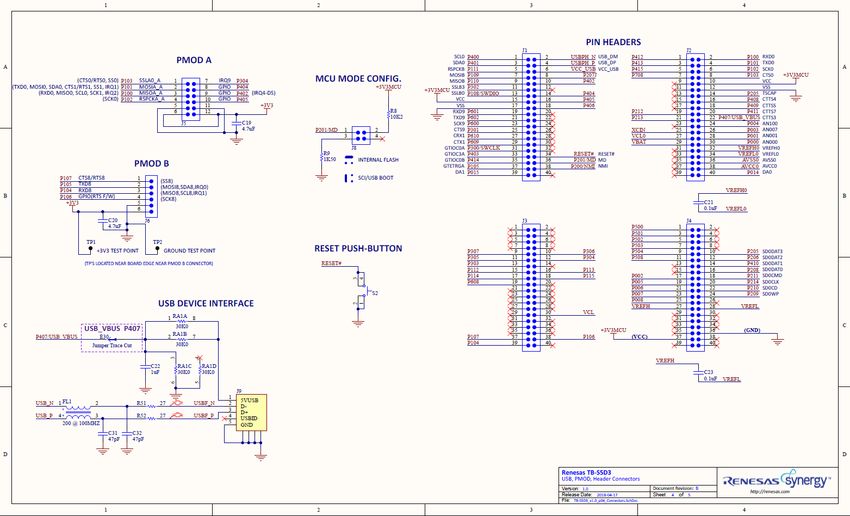
5.4 Connectivity and Settings
Throughout this section, feature configuration using copper jumpers is described. See Section 4.1.1, Copper
Jumpers for information on using copper jumpers.
5.4.1 Device USB
The DEVICE USB Micro-B connection jack connects the Main MCU to an external
USB Host, FS capable, allowing communications for testing and use of the Main
MCU firmware. Power for the Target Board cannot be received from this connector.
The DEVICE USB interface can detect the presence of power from the USB Host
PC. USB Host power received at the DEVICE USB interface is not connected to
the Target Board 5 V power bus.
Table 2. DEVICE USB Connector (J9)
USB Device Connector TB-S5D3
Pin Description Signal/Bus
+5VDC, connected to a sense voltage 2/3 divider to allow +5VUSB
1
Main MCU sensing of Host presence P407/USB_VBUS = 2/3(5VUSB)
2 Data- P915/USB_DM
3 Data+ P914/USB_DP
4 USB ID, jack internal switch, cable inserted N.C.
5 Ground GND
Connections in Table 2 are based on the condition of
copper jumpers E16, E17, E20, E21, and E30 matching
their default state. By default, E16 and E17 are closed,
E20 and E21 are open, and E30 is closed.
Alternatively, the Device USB signals to the Main MCU may be connected to MCU Pin Header J1. To enable
this configuration, copper jumpers E16 and E17 should be open, and E20 and E21 should be closed.
5.4.2 Debug USB
The DEBUG USB Micro-B connection jack connects the S124 J-Link MCU to an
external USB Host, FS capable, allowing re-programming and debugging of the Main
MCU firmware. Power for the Target Board may be received from this connector.
The J-Link® OB interface is multiplexed with the JTAG interface and can
collectively be referred to as the Programming Interface. While the J-Link® OB
interface and the JTAG interface do not conflict, the J-Link® OB signals may be
isolated from the programming interface by changing the associated copper
jumpers.
J-Link Disconnect Copper Jumpers E32, E33, E34, E37, and E38 connect the J-
Link signals to the MCU programming interface. To isolate the J-Link signals from
the JTAG interface, these copper jumpers must be open. To allow use of the
J-Link interface, each copper jumper must be closed.
J-Link MCU Power Copper Jumper, E1, connects the main +3.3 V power to the J-
Link +3.3 V power. The default condition for E1 is closed, which connects the J-Link
MCU power to the main +3.3 V power. If J-Link signals are disconnected, the power
to the J-Link MCU should also be removed by changing E1 to open.
R12UM0032EU0101 Rev.1.01 Page 15 of 38
Feb.08.19Renesas Synergy™ Platform Target Board Kit S5D3 (TB-S5D3) Table 3. DEBUG USB Connector (J11) DEBUG USB Connector TB-S5D3 Pin Description Signal/Bus 1 +5VDC +5V_JUSB 2 Data- U2 USB_DM (U2-18) 3 Data+ U2 USB_DP (U2-19) 4 USB ID, jack internal switch, cable inserted N.C. 5 Ground GND Three of the J-Link ports (P108, P109, and P300) conflict with the SPI interface, as shown in the following table. Table 4. J-Link Interface Conflicts Programming Interface Conflicting Interface Port Use Interface Use P108 SWDIO/JTAG TMS SPI SSLB0 fixed function, J1-13 P109 SWO/JTAG TDO SPI MOSIB fixed function, J1-7 P300 SWCLK/JTAG TCK GPT GTIOC0A fixed function, J1-31 5.4.3 JTAG/SWD A 10-pin Cortex® Debug Connector is provided at J10. Table 5. JTAG/SWD Connector (J10) JTAG Connector TB-S5D3 Pin JTAG pin name SWD pin name Signal/Bus 1 VTref VTref +3V3 2 TMS SWDIO U1 P108/SWDIO (U1-51) 3 GND GND GND 4 TCK SWCLK U1 P300/SWCLK (U1-50) 5 GND GND GND 6 TDO SWO U1 P109 (U1-52) 7 Key Key N.C. 8 TDI NC/EXTb U1 P110 (U1-53) 9 GNDDetect GNDDetect N.C. (short E31 to connect to GND) 10 nSRST nSRST U1 RESET# (U1-38) The Cortex® Debug Connector is fully described in the Arm® CoreSight™ Architecture Specification. The J-Link MCU Power copper jumper and J-Link Disconnects copper jumpers may be open for proper operation of the JTAG interface to prevent interactions with the J-Link MCU. See section 5.4.2 for details. If a JTAG adapter is in use that properly interprets the Arm® Cortex® 10-pin Debug Connector assignment of pin 9 to GND, JTAG GNDDetect copper jumper E31 should be closed. If the JTAG adapter used is one of several that may be confused or damaged by the presence of GND at pin 9, E31 should be open (as shipped). The J-Link® OB interface is multiplexed with the JTAG interface and can collectively be referred to as the Programming Interface. While the J-Link® OB interface and the JTAG interface do not conflict, the J-Link® OB signals may be isolated from the programming interface by changing the copper jumpers as described in section 5.4.2, Debug USB. R12UM0032EU0101 Rev.1.01 Page 16 of 38 Feb.08.19
Renesas Synergy™ Platform                                          Target Board Kit S5D3 (TB-S5D3)
Four of the JTAG ports (P108, P109, P110 and P300) conflict with the SPI interface, as shown in the
following table.
Table 6. JTAG Interface Conflicts
 Programming Interface                 Conflicting Interface
 Port      Use                         Interface      Use
 P108      TMS/J-Link SWDIO            SPI            SSLB0_B fixed function, J1-13
 P109      TDO/J-Link SWO              SPI            MOSIB_B fixed function, J1-7
 P110      TDI                         SPI            MISOB_B fixed function, J1-9
 P300      SWCLK                       GPT            GTIOC0A_A fixed function, J1-31
5.4.4   LEDs
Two LEDs are provided on the TB-S5D3. Target Board U1 is the Main MCU, and directly controls LED1. See
Figure 7 for LED1 location, Figure 10 for LED2 location, and Figure 9 for LED2 circuit. Target Board U2 is
the J-Link MCU and controls the red LED in LED2.

                                     Figure 14. LED1 Control Circuit
The behavior of the LEDs is described in the following table.
Table 7. Target Board LED Functions
Designator         Color           Function                     MCU control port      MCU pin
LED1               Red             User LED                     U1 P112               U1-55
LED2               Red             J-Link Indicator             JLED (U2 P103)        U2-45
LED2               Green           3.3 V Power Available        +3V3                  N.A.

To disconnect the User LED from the MCU signal P112, copper jumper E3 must be open.

5.4.5   Switches
Two miniature, momentary, mechanical push-button type SMT switches are mounted on
the Target Board. Pressing the RESET Switch generates a reset signal to restart the Main
MCU. To disconnect the User Switch from the MCU signal P415/IRQ8, copper jumper E4
must be open.
Table 8. Target Board Switches
 Designator         Function                 MCU Control Port      MCU Pin
 S1                 User Switch              U1 P415/IRQ8          U1-17
 S2                 MCU Reset Switch         RESET#                U1-38

R12UM0032EU0101 Rev.1.01                                                                     Page 17 of 38
Feb.08.19
Renesas Synergy™ Platform Target Board Kit S5D3 (TB-S5D3)
Figure 15. User Switch Circuit
Figure 16. User Switch (S1) on the Target Board
Figure 17. Reset Switch Circuit
Figure 18. Reset Switch (S2) on the Target Board
R12UM0032EU0101 Rev.1.01 Page 18 of 38
Feb.08.19Renesas Synergy™ Platform Target Board Kit S5D3 (TB-S5D3) 5.4.6 PMOD A A 12-pin PMOD type 2A connector is provided at PMOD A. The interface is powered for 3.3 V modules only. The Main MCU acts as the SPI master, and the connected module acts as an SPI slave device. This interface may additionally be re-configured in firmware as several other PMOD types. Signals on PMOD A are shared with Main MCU Pin Header J1 and J2. Care must be taken to ensure that shared signals are not used concurrently. Table 9. PMOD A Connector (J5) PMOD A connector TB-S5D3 Pin Description Signal/Bus 1 SS (low to select slave) U1 P103, SSLA0_A (U1-72) 2 MOSI U1 P101, MOSIA_A (U1-74) 3 MISO U1 P100, MISOA_A (U1-75) 4 SCK U1 P102, RSPCKA_A (U1-73) 5 GND GND 6 VCC +3V3 7 INT (slave to master) U1 P304, IRQ1 (U1-44) 8 RESET (master to slave) U1 P404, GPIO (U1-5) 9 Not Specified U1 P402, GPIO (U1-3) 10 Not Specified U1 P405, GPIO (U1-6) 11 GND GND 12 VCC +3V3 Limits of the 3.3 V regulator on the Target Board, and limits of the power source supplying that regulator (especially for USB Host devices), including the to-be-connected PMOD device, must be considered prior to connecting a module to a PMOD connector. 5.4.7 PMOD B A 6-pin PMOD type 4 connector is provided at PMOD B. The interface is powered for 3.3 V modules only. The Main MCU acts as the UART DCE, and the connected module acts as the UART DTE. This interface may additionally be re-configured in firmware as some other PMOD type. Signals on PMOD B are shared with Main MCU Pin Header J1 and J2. Care must be taken to ensure that shared signals are not used concurrently. Table 10. PMOD B Connector (J6) PMOD B Connector TB-S5D3 Pin Description Signal/Bus 1 CTS (from module) U1 P107, CTS8 (U1-68) 2 TXD U1 P105, TXD8 (U1-70) 3 RXD U1 P104, RXD8 (U1-71) 4 RTS (from Main MCU) U1 P106, GPIO (U1-69) (for RTS by Main MCU firmware) 5 GND GND 6 VCC +3V3 Limits of the 3.3 V regulator on the Target Board, and limits of the power source supplying that regulator (especially for USB Host devices), including the to-be-connected PMOD device, must be considered prior to connecting a module to a PMOD connector. 5.4.8 User Capacitive Touch Button A capacitive sensor region for use as a Capacitive Touch button is provided in the board USER INPUT region. A support circuit, TSCAP, is required for proper operation of Capacitive Touch button(s) by the Main MCU. To disconnect the Capacitive Touch Button from the MCU, copper jumper E2 must be open. To connect MCU signal P207 to Pin Header J1, copper jumper E5 must be closed. R12UM0032EU0101 Rev.1.01 Page 19 of 38 Feb.08.19
Renesas Synergy™ Platform                                     Target Board Kit S5D3 (TB-S5D3)
Table 11. Target Board Capacitive Touch Button Sensor
 Designator   Function                    MCU Control Port       MCU Pin
 TS1          Capacitive Touch Button     U1 P207 (TS2)          U1-30
 -            TSCAP Support               U1 P205 (TSCAP-A)      U1-32

                            Figure 19. Capacitive Touch Button Circuit

                            Figure 20. Capacitive Touch TSCAP Circuit

                Figure 21. Capacitive Touch Button on the Target Board (Top Side)

R12UM0032EU0101 Rev.1.01                                                            Page 20 of 38
Feb.08.19
Renesas Synergy™ Platform Target Board Kit S5D3 (TB-S5D3)
5.5 Target Board Pin Headers
The Target Board Pin Headers J1, J2, J3, and J4, provide access to all Main MCU interface signals, and to
voltages for all Main MCU power ports.
Fixed Function Pin Assignments
For consistency across all Synergy Target Board Kits, some pin assignments on the headers have fixed
function signal assignments. This provides specific signals and functions to be at a common pin header
location on all Target Boards for a particular Synergy MCU group (for example, S1/S3/S5/S7) and, where
possible, across all Synergy Target Boards.
On the TB-S5D3 board, 40 pins of the pin headers are set aside for fixed function assignment. These pins
are odd-numbered pins of J1 and even-numbered pins of J2.
Pin Header Fixed Function Pins are labeled on the Target Board with dark text on a white background. Pins
that are not Fixed Function pins are labeled with white text on a dark background. On the top side of the
board is the functional label for the fixed location. On the bottom side of the board is the port information for
the same pin.
Figure 22. Fixed Function Pin Label Example
There are several pins in the headers that are Secondary Fixed Function Pins. These Secondary Fixed
Function Pins share common pin assignments with other Target Boards that have Main MCUs with the same
functionality. The Secondary Fixed Function Pins are also labeled with the top side having a functional label,
and the bottom side having a port label.
R12UM0032EU0101 Rev.1.01 Page 21 of 38
Feb.08.19Renesas Synergy™ Platform Target Board Kit S5D3 (TB-S5D3)
Figure 23. TB-S5D3 Pin Headers Circuit
R12UM0032EU0101 Rev.1.01 Page 22 of 38
Feb.08.19Renesas Synergy™ Platform Target Board Kit S5D3 (TB-S5D3) 5.5.1 Pin Header J1 Pin Header J1 is a 2-column by 20-row through-hole header on 2.54 mm centers. Table 12. Pin Header J1 Pin Assignment 100p S5D3 Pin S5D3 Signal J1 Pins S5D3 Signal 100p S5D3 Pin 1 P400 1 2 USBPH_N 27 2 P401 3 4 USBPH_P 28 54 P111 5 6 VCC_USB 29 52 P109 7 8 P207J 30 53 P110 9 10 P402 3 48 P302 11 12 (None) NC 51 P108 13 14 P404 5 15 VCC 15 16 P405 6 12 VSS 17 18 P406 7 66 P601 19 20 (None) NC 65 P602 21 22 (None) NC 67 P600 23 24 (None) NC 49 P301 25 26 (None) NC 61 P610 27 28 (None) NC 60 P609 29 30 (None) NC 50 P300 31 32 (None) NC 4 P403 33 34 RESET# 38 18 P414 35 36 P201 39 18 P105 37 38 P200 40 84 P015 39 40 (None) NC Color Key Primary Fixed Function Pins Secondary Fixed Function Pins R12UM0032EU0101 Rev.1.01 Page 23 of 38 Feb.08.19
Renesas Synergy™ Platform                                       Target Board Kit S5D3 (TB-S5D3)
5.5.2   Pin Header J2
Pin Header J2 is a 2-column by 20-row through-hole header on 2.54 mm centers.
Table 13. Pin Header J2 Pin Assignment

100p S5D3 Pin S5D3 Signal                    J2 Pins          S5D3 Signal       100p S5D3 Pin
20             P412                          1         2      P100              75
19             P413                          3         4      P101              74
17             P415                          5         6      P102              73
16             P708                          7         8      P103              72
NC             (None)                        9         10     VCC               46
NC             (None)                        11        12     VSS               45
NC             (None)                        13        14     P205              32
NC             (None)                        15        16     P408              24
NC             (None)                        17        18     P409              23
14             P212                          19        20     P411              21
13             P213                          21        22     P407/USB_VBUS     25
NC             (None)                        23        24     P004              96
10             XCIN                          25        26     P003              97
9              VCL0                          27        28     P001              99
8              VBAT                          29        30     P000              100
NC             (None)                        31        32     VREFH0            91
NC             (None)                        33        34     VREFL0            90
NC             (None)                        35        36     AVSS0             89
NC             (None)                        37        38     AVCC0             88
NC             (None)                        39        40     P014              85
Color Key
Primary Fixed Function pins
Secondary Fixed Function pins

R12UM0032EU0101 Rev.1.01                                                              Page 24 of 38
Feb.08.19
Renesas Synergy™ Platform                                       Target Board Kit S5D3 (TB-S5D3)
5.5.3   Pin Header J3
Pin Header J3 is a 2-column by 20-row through-hole header on 2.54 mm centers.
Table 14. Pin Header J3 Pin Assignment

100p S5D3 Pin S5D3 Signal              J3 Pins              S5D3 Signal             100p S5D3 Pin
NC             (None)                  1          2         (None)                  NC
NC             (None)                  3          4         (None)                  NC
NC             (None)                  5          6         (None)                  NC
NC             (None)                  7          8         (None)                  NC
41             P307                    9          10        P306                    42
43             P305                    11         12        P304                    44
47             P303                    13         14        (None)                  NC
55             P112                    15         16        P113                    56
57             P114                    17         18        P115                    58
59             P608                    19         20        (None)                  NC
NC             (None)                  21         22        (None)                  NC
NC             (None)                  23         24        (None)                  NC
NC             (None)                  25         26        (None)                  NC
NC             (None)                  27         28        (None)                  NC
NC             (None)                  29         30        VCL                     64
NC             (None)                  31         32        (None)                  NC
NC             (None)                  33         34        (None)                  NC
NC             (None)                  35         36        (None)                  NC
68             P107                    37         38        P106                    69
71             P104                    39         40        (None)                  NC
Color Key
Secondary Fixed Function pins

R12UM0032EU0101 Rev.1.01                                                            Page 25 of 38
Feb.08.19
Renesas Synergy™ Platform                                       Target Board Kit S5D3 (TB-S5D3)
5.5.4   Pin Header J4
Pin Header J4 is a 2-column by 20-row through-hole header on 2.54 mm centers.
Table 15. Pin Header J4 Pin Assignment

100p S5D3 Pin S5D3 Signal              J4 Pins              S5D3 Signal             100p S5D3 Pin
76              P500                   1          2         (None)                  NC
77              P501                   3          4         (None)                  NC
78              P502                   5          6         (None)                  NC
79              P503                   7          8         (None)                  NC
80              P504                   9          10        P205                    32
881             P508                   11         12        P206                    32
NC              (None)                 13         14        P410                    22
NC              (None)                 15         16        P208                    37
98              P002                   17         18        P211                    34
95              P005                   19         20        P214                    33
94              P006                   21         22        P210                    35
93              P007                   23         24        P209                    36
92              P008                   25         26        (None)                  NC
87              VREFH                  27         28        VREFL                   86
NC              (None)                 29         30        (None)                  NC
NC              (None)                 31         32        (None)                  NC
NC              (None)                 33         34        (None)                  NC
NC              (None)                 35         36        GND                     63
62              VCC                    37         38        (None)                  NC
NC              (None)                 39         40        (None)                  NC
Color Key
Secondary Fixed Function pins

R12UM0032EU0101 Rev.1.01                                                            Page 26 of 38
Feb.08.19
Renesas Synergy™ Platform Target Board Kit S5D3 (TB-S5D3)
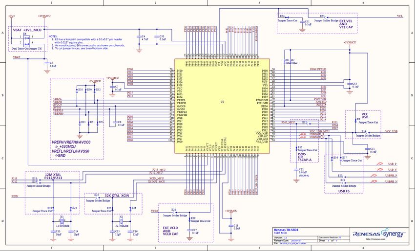
5.6 Additional Features
5.6.1 Reference Voltages VREF and VREF0
Capacitor C21 provides noise-bypass capability for VREFH0 and VREFL0, and
capacitor C23 provides noise-bypass capability for VREFH and VREFL. See
Figure 23 for the circuit design.
By default, VREFH and VREFH0 are connected to the MCU supply voltage
(+3V3MCU) and VREFL and VREFL0 are connected to the system ground.
To disconnect VREFH from the MCU supply voltage, E52 must be open. To
disconnect VREFL from the system ground, E53 must be open. To disconnect
VREFH0 from the MCU supply voltage, E50 must be open. To disconnect
VREFL0 from the system ground, E51 must be open. See Figure 24 for the
circuit design.
5.6.2 Analog Voltage AVCC0/AVSS0
By default, AVCC0 is connected to the MCU supply voltage (+3V3MCU) and AVSS0 is connected to the
system ground.
To disconnect these references from the AVCC0 and AVSS0 lines, copper jumpers E10 and E11 must be
open.
See Figure 24 for the circuit design.
Figure 24. Analog and Reference Voltages
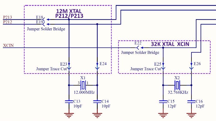
5.6.3 On-Board Clock Crystals
The TB-S5D3 includes two precision crystal clock sources. A precision
12.000 MHz crystal is installed at location X1, and a precision 32.768 kHz
crystal is installed at location X2. These crystal clock sources are connected
to the Main MCU by default.
The MCU pins for the 12 MHz clock crystal may be connected to P212 and
P213. To disconnect the 12 MHz crystal, open copper jumpers E23 and E24,
and close copper jumpers E18 and E19.
The 32.768 kHz clock crystal may be replaced by an external clock source
connected to XCIN. To disconnect the 32.768 kHz crystal, open copper
jumpers E25 and E26, and close copper jumper E22.
R12UM0032EU0101 Rev.1.01 Page 27 of 38
Feb.08.19Renesas Synergy™ Platform Target Board Kit S5D3 (TB-S5D3)
Figure 25. Crystal Clock Sources
5.6.4 User Potentiometer
A footprint for installation of a potentiometer and a recommended noise-bypass capacitor are
provided on the Target Board. The footprint was designed for installation of a Bourns P/N 3352T-1-
103LF, or equivalent, as the potentiometer, and a Samsung P/N CL10B104KB8NNNC, or similar, as
the noise-bypass capacitor.
When the User Potentiometer is installed, copper jumper E36 must be closed to connect the User
Potentiometer to the MCU.
Table 16. Target Board User Potentiometer
Designator Function MCU Control Port MCU Pin
POT1 User Potentiometer U1 P004 (AN100) U1-96
Figure 26. User Potentiometer Circuit
Figure 27. User Potentiometer on the Target Board (Top Side)
R12UM0032EU0101 Rev.1.01 Page 28 of 38
Feb.08.19Renesas Synergy™ Platform Target Board Kit S5D3 (TB-S5D3)
5.6.5 Boot Configuration
The BOOT CONFIG jumper, J8, is used to configure the operating mode of the S5D3 MCU at boot.
Table 17. Boot Configuration
Boot Configuration J8 Shunt Location
Normal Boot (default) Pins 1 and 2
SCI/USB Boot Pins 1 and 3
Figure 28. Boot Config Jumper J8
5.6.6 Miscellaneous Signals
5.6.6.1 VCL
By default, the Main MCU pin VCL is connected to reference capacitor C51.
To connect this pin to MCU Pin Header J3, solder bridge E55 must be closed.
To disconnect the reference capacitor C51, copper jumper E54 must be open.
Figure 29. VCL and VCL Capacitor
R12UM0032EU0101 Rev.1.01 Page 29 of 38
Feb.08.19Renesas Synergy™ Platform Target Board Kit S5D3 (TB-S5D3)
5.6.6.2 VCC_USB
By default, the Main MCU pin VCC_USB is connected to the +3V3 MCU supply voltage.
Alternatively, this pin may be connected to MCU Pin Header J1. To do this, copper jumper
E8 must be open, and copper jumper E14 must be closed.
Figure 30. VCC_USB Circuit
5.6.6.3 Signal P205
By default, the Main MCU pin P205 is connected to a TSCAP-A capacitor. This pin may
be connected to MCU Pin Header J2. To do this, copper jumper E12 must be closed.
The TSCAP-A capacitor may be disconnected by making copper jumper E15 open.
Figure 31. P205 Circuit
R12UM0032EU0101 Rev.1.01 Page 30 of 38
Feb.08.19Renesas Synergy™ Platform Target Board Kit S5D3 (TB-S5D3) 6. Electrical Schematics R12UM0032EU0101 Rev.1.01 Page 31 of 38 Feb.08.19
Renesas Synergy™ Platform   Target Board Kit S5D3 (TB-S5D3)

R12UM0032EU0101 Rev.1.01                        Page 32 of 38
Feb.08.19
Renesas Synergy™ Platform   Target Board Kit S5D3 (TB-S5D3)

R12UM0032EU0101 Rev.1.01                        Page 33 of 38
Feb.08.19
Renesas Synergy™ Platform   Target Board Kit S5D3 (TB-S5D3)

R12UM0032EU0101 Rev.1.01                        Page 34 of 38
Feb.08.19
Renesas Synergy™ Platform   Target Board Kit S5D3 (TB-S5D3)
7.   Mechanical Drawing

R12UM0032EU0101 Rev.1.01                        Page 35 of 38
Feb.08.19
Renesas Synergy™ Platform                                           Target Board Kit S5D3 (TB-S5D3)
8. Certifications
FCC Compliance
This device complies with part 15 of the FCC Rules. Operation is subject to the following two conditions: (1)
This device may not cause harmful interference, and (2) this device must accept any interference received,
including interference that may cause undesired operation.
China SJ/T 113642014, 10year environmental protection use period.

EU RoHS

EU EMI/EMC compliance

R12UM0032EU0101 Rev.1.01                                                                        Page 36 of 38
Feb.08.19
Renesas Synergy™ Platform                                        Target Board Kit S5D3 (TB-S5D3)
Website and Support
Visit the following vanity URLs to learn about key elements of the Synergy Platform, download components
and related documentation, and get support.

Synergy Software                       www.renesas.com/synergy/software
       Synergy Software Package        www.renesas.com/synergy/ssp
       Software add-ons                www.renesas.com/synergy/addons
       Software glossary               www.renesas.com/synergy/softwareglossary
       Development tools               www.renesas.com/synergy/tools

Synergy Hardware                       www.renesas.com/synergy/hardware
       Microcontrollers                www.renesas.com/synergy/mcus
       MCU glossary                    www.renesas.com/synergy/mcuglossary
       Parametric search               www.renesas.com/synergy/parametric
       Kits                            www.renesas.com/synergy/kits

Synergy Solutions Gallery              www.renesas.com/synergy/solutionsgallery
       Partner projects                www.renesas.com/synergy/partnerprojects
       Application projects            www.renesas.com/synergy/applicationprojects

Self-service support resources:
        Documentation                  www.renesas.com/synergy/docs
        Knowledgebase                  www.renesas.com/synergy/knowledgebase
        Forums                         www.renesas.com/synergy/forum
        Training                       www.renesas.com/synergy/training
        Videos                         www.renesas.com/synergy/videos
        Chat and web ticket            www.renesas.com/synergy/resourcelibrary

R12UM0032EU0101 Rev.1.01                                                                    Page 37 of 38
Feb.08.19
You can also read