EFFICIENT "GREEN" QUANTUM DOT-S SENSITIZED SOLAR CELLS BASE BASED ON CU2S/CUINS2/ZNSE ARCHITECTURE
←
→
Page content transcription
If your browser does not render page correctly, please read the page content below
Electronic Supplementary Material (ESI) for Chemical Communications
This journal is © The Royal Society of Chemistry 2012

                       Efficient “Green” Quantum Dot-s Sensitized Solar Cells

                               base based on Cu2S/CuInS2/ZnSe Architecture
                        Jia-Yaw Chang,* Li-Fong Su, Chen-Hei Li, Chia-Chan Chang, and Jie-Mo Lin

                                                E-mail: jychang@mail.ntust.edu.tw

                    Department of Chemical Engineering, National Taiwan University of Science and

                   Technology, Taipei, Taiwan

                   Experimental Section
                   1. Materials
                   Copper(II) nitrate hemipentahydrate (Cu(NO3)2, 98%) and selenium(IV) oxide (SeO2,
                   99.4%) were purchased from Alfa-Aesar (Ward Hill, USA). Indium(III) nitrate
                   hydrate (In(NO3)3, 99.4%) and sulfur powder (S, 99.98%) was purchased from
                   Sigma-Aldrich (Milwaukee, USA). Sodium borohydride (99.8+%), potassium
                   chloride (99+%), sodium sulfide nonhydrate (Na2S, 98+%) was purchased from Acros
                   Organics (New Jersey, USA), Zinc acetate dihydrate (ZnAc2, 99.8%) was obtained
                   from J.T. Baker (Phillipsburg, USA). All organic solvents were purchased from EM
                   Sciences. All chemicals were used directly without further purification.
                   2. Device Fabrication.
                   2.1. Preparation of TiO2 Electrodes.
                   Prior to the fabrication of TiO2 films, fluorine-doped tin oxide (FTO) glass was
                   ultrasonically cleaned sequentially for 30 min each in HCl, acetone, ethanol, and
                   water. Mesoscopic TiO2 films were prepared by screen printing of a TiO2 slurry
                   (Solaronix) on the FTO glass. A paste for the scattering layer containing anatase TiO2
                   particles was deposited by screen printing, resulting in light-scattering TiO2 films.
                   This was followed by sintering at 500 °C for 30 min.
                   2.2. Deposition of Cu2S Buffer Layer on TiO2 Electrodes
                   To deposit Cu2S buffer layer on the TiO2 electrodes, as-prepared TiO2 electrodes were
                   immersed in a solution of 1.25×10⁻³ M Cu(NO3)2 for 30 s. They were then rinsed and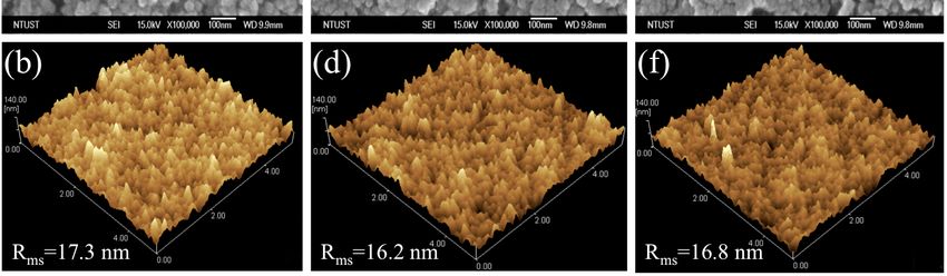
Electronic Supplementary Material (ESI) for Chemical Communications
This journal is © The Royal Society of Chemistry 2012

                   immersed in a solution of 0.135 M Na2S for another 4 min, followed by another
                   rinsing.
                   2.3. Deposition of CuInS2 Sensitizer on TiO2/Cu2S Electrodes
                   TiO2/Cu2S electrodes prepared by the above-described procedure were successively
                   exposed to three different solutions: one of 0.10 M In(NO3)3 for 60 s, another of
                   1.25×10⁻³ M Cu(NO3)2 for 30 s, and a final one of 0.135 M Na2S for 4 min. After
                   each immersion procedure, the electrode was rinsed for 1 min to remove the excess
                   precursor solution. This SILAR process was repeated for several cycles (between two
                   and seven) until the desired CuInS2-coated TiO2 electrode was achieved. A sample
                   that went through n SILAR cycles of CuInS2 QD deposition is denoted as
                   Cu2S/CuInS2(n).
                   2.4. Deposition of ZnS or ZnSe Passivation Layer on TiO2/CuS/CuInS2(6)
                   Electrodes
                   For ZnS passivation, the TiO2/Cu2S/CuInS2(6) electrode was successively exposed for
                   1 min each to solutions of 0.1 M ZnAc2 and 0.1 M Na2S. After each immersion
                   procedure, the electrode was rinsed for 1 min to remove the excess precursor solution.
                   This SILAR process was repeated several cycles until the desired ZnS passivation on
                   the TiO2/Cu2S/CuInS2 electrode was achieved. For ZnSe passivation, the
                   TiO2/Cu2S/CuInS2(6) electrode was successively exposed for 1 min each to 0.1 M
                   ZnAc2 and a 0.1 M Se precursor solution. The Se precursor solution was prepared by
                   heating a mixture of 0.12 M SeO2 and 1.2 M NaBH4 according to a modified version
                   of a previously published procedure.1 After each immersion procedure, the electrode
                   was rinsed to remove excess precursor solution. This SILAR process was repeated for
                   several cycles until the desired ZnSe passivation layer on the TiO2/Cu2S/CuInS2(6)
                   electrode was achieved.
                   2.5. QD-Sensitized Solar Cell Configuration.
                   After preparing the QD-sensitized TiO2 electrode by the SILAR process described
                   above, the solar cells were assembled by placing a platinum-deposited conducting
                   glass (counter electrode) prepared by thermal evaporation on the QD-sensitized TiO2
                   electrode by using a 60-μm-thick Surlyn sheet (DuPont 1702) as a spacer. The
                   polysulfide redox electrolyte—prepared by mixing 1.8 M Na2S, 2.0 M sulfur, and 0.2
                   M potassium chloride—was introduced into the sealed cell through a hole pre-drilled
                   in the counter electrode. The active area of the cell was 0.16 cm2.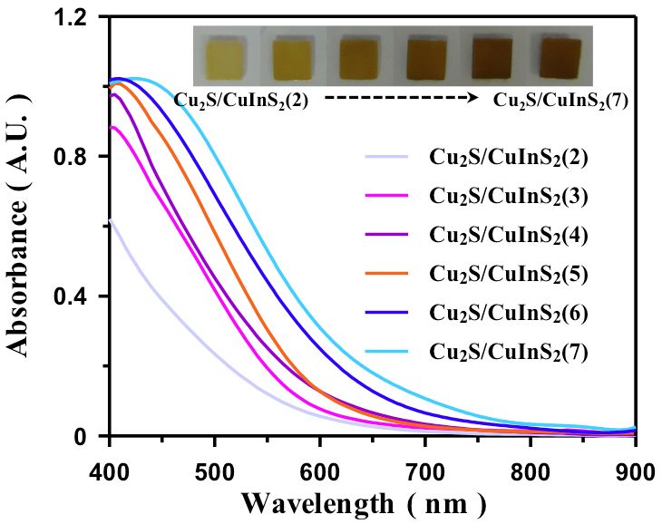
Electronic Supplementary Material (ESI) for Chemical Communications
This journal is © The Royal Society of Chemistry 2012

                   2.6. Sample Characterization
                   The field emission scanning electron microscopy (SEM) was performed on a JEOL
                   6335F (JEOL USA Inc., USA) equipped with an energy dispersive X-ray (EDX)
                   analysis. The high-resolution transmission electron microscopy (TEM) images of the
                   nanocrystals was examined by field-emission TEM on a Philips Tecnai G2 F20
                   microscope (Philips, Holland). Atomic force microscopy (AFM) observation was
                   conducted using an SPM-9600 scanning probe microscope (Shimadzu Co.) at room
                   temperature. The root mean square (Rms) was used to evaluate the surface roughness
                   of the QD films on the basis of a 5.0 μm × 5.0 μm scan area. UV-vis–near infrared
                   (NIR) absorption spectra were measured with a JASCO V-670 spectrometer. X-ray
                   photoelectron spectroscopy (XPS) was performed by using a VG ESCA scientific
                   theta probe spectrometer in constant analyzer energy mode with a pass energy of 28
                   eV and Al Ka (1486.6 eV) radiation as the excitation source. The photocurrent
                   density-photovoltage characteristics of the QD-sensitized solar cell were recorded
                   under the illumination provided by a solar simulator (Oriel 6691 450-W xenon arc
                   lamp, CT, USA) at 100% sunlight (AM 1.5, 100 mW/cm2). A mask with a window of
                   0.16 cm2 was clipped on the TiO2 side to define the active area of the cell. The
                   incident photon to current conversion efficiency (IPCE) plotted as a function of
                   excitation wavelength was measured with a PEC-S20 instrument (Peccell
                   Technologies, Inc., Kanagawa, Japan). Electrochemical impedance spectra (EIS) were
                   measured by using an impedance analyzer (Auto Lab PGSTAT320N) at open-circuit
                   potentials under 1 sun of illumination, with the magnitude and frequency of the
                   alternative signal being 10 mV and 10-1–105 Hz, respectively.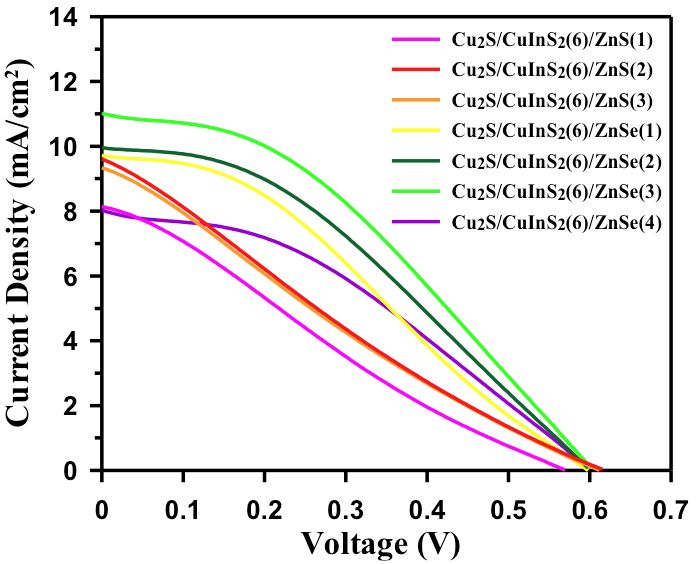
Electronic Supplementary Material (ESI) for Chemical Communications
This journal is © The Royal Society of Chemistry 2012

                   Fig. S1. Absorption spectra of Cu2S/CuInS2 sensitized TiO2 film at different numbers
                   of CuInS2 SILAR cycles. A sample after m cycles of CuInS2 QD deposition is
                   denoted as Cu2S/CuInS2(m). Inset shows a photograph of the corresponding sample
                   deposited on TiO2 film.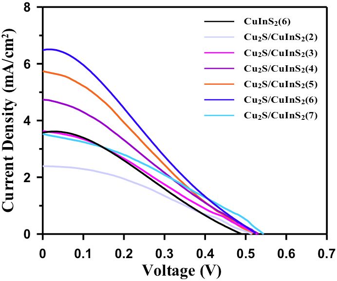
Electronic Supplementary Material (ESI) for Chemical Communications
This journal is © The Royal Society of Chemistry 2012

                   Fig. S2. Photocurrent density-voltage characteristic curves of QD-sensitized solar cell
                   at different numbers of CuInS2 SILAR cycles.

                   Table S1. Summary of photovoltaic properties of QD-sensitized solar cells fabricated
                   with different sensitization conditions.

                   Sample                           JSC (mA cm-2)     VOC (mV)   FF (%)         η (%)
                   CuInS2(6)                              3.65         479.8      30.3           0.53
                   Cu2S/CuInS2(2)                         2.38         509.7      34.8           0.42
                   Cu2S/CuInS2(3)                         3.63         524.6      29.3           0.56
                   Cu2S/CuInS2(4)                         4.75         529.7      27.3           0.69
                   Cu2S/CuInS2(5)                         5.74         519.9      26.9           0.80
                   Cu2S/CuInS2(6)                         6.58         529.9      25.9           0.90
                   Cu2S/CuInS2(7)                         3.53         544.9      32.9           0.63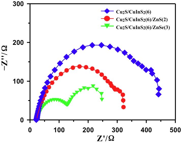
Electronic Supplementary Material (ESI) for Chemical Communications
This journal is © The Royal Society of Chemistry 2012

                   Fig. S3. Photocurrent density-voltage characteristic curves of Cu2S/CuInS2(6) QD-
                   sensitized solar cell at different numbers of ZnS or ZnSe SILAR cycles.

                   Table S2. Summary of photovoltaic properties of the Cu2S/CuInS2(6) QD-sensitized
                   solar cell at different numbers of ZnS or ZnSe SILAR cycles.

                   Sample                           JSC (mA cm-2)     VOC (mV)    FF (%)     η (%)
                   Cu2S/CuInS2(6)/ZnS(1)                  8.16         574.9       24.7      1.10
                   Cu2S/CuInS2(6)/ZnS(2)                  9.62         614.9       24.1      1.33
                   Cu2S/CuInS2(6)/ZnS(3)                  9.38         609.8       24.3      1.29
                   Cu2S/CuInS2(6)/ZnSe(1)                 9.72         600.0       36.7      2.02
                   Cu2S/CuInS2(6)/ZnSe(2)                 9.97         605.0       40.6      2.27
                   Cu2S/CuInS2(6)/ZnSe(3)                10.96         604.9       40.6      2.52
                   Cu2S/CuInS2(6)/ZnSe(4)                 7.98         599.9       42.5      1.80
Electronic Supplementary Material (ESI) for Chemical Communications
This journal is © The Royal Society of Chemistry 2012
Fig. S4. XPS spectra of Cu2S/CuInS2/ZnSe QD-sensitized solar cell. The Cu 2p core
splits into 2p3/2 (932.8 eV) and 2p1/2 (952.7 eV) peaks, consistent with the standard
separation of 19.9 eV (Fig. S4a).2 In addition, the Cu 2p3/2 satellite peak of Cu(II),
which is usually located at 942 eV3, does not appear in the spectrum. Therefore, it can
be concluded that only monovalent copper exists in the sample. The binding energies
of In 3d5/2 and In 3d3/2 can be assigned to 444.9 eV and 452.4 eV, respectively (Fig.
S4b). The S 2p1/2 peak at 161.1 eV can be assigned to the S coordinated to Cu and In
(Fig. S4c). The peaks of Zn 2p appear at binding energies of 1022.6 and 1045.7 eV,
which can be assigned to Zn(II) with a peak splitting of 23.1 eV4 (Fig. S4d). The Se
3d peak at 55.3 eV (Fig. S4c) and the Se 3p core located at 167.0 eV (Fig. S4e),
which are in good accordance with values reported previously, were assigned to Se
3p1/2.2,5Electronic Supplementary Material (ESI) for Chemical Communications
This journal is © The Royal Society of Chemistry 2012
Fig. S5. EIS spectra of QD-sensitized solar cells fabricated with different sensitization
conditions.Electronic Supplementary Material (ESI) for Chemical Communications
This journal is © The Royal Society of Chemistry 2012
Fig. S6. SEM (top panels) and AFM images (bottom panels) of the (a, b)
Cu2S/CuInS2(6), (c, d) Cu2S/CuInS2(6)/ZnS(2), and (e, f) Cu2S/CuInS2(6)/ZnSe(3)
configurations prepared by the SILAR process.
(a) Ti (b) S
Ti
Intensity
Intensity
S
O
O In
Zn In
Pt In
Cu In Ti Pt
Pt Cu Pt Ti
0 1 2 3 4 5 6 7 8 9 0 1 2 3 4 5 6 7 8 9
Energy ( KeV ) Energy ( KeV )
(c)
Intensity
Ti
O S
Se In
Zn
Cu Pt In
Ti
0 1 2 3 4 5 6 7 8 9
Energy ( KeV )
Fig. S7. EDX spectrum of the (a) Cu2S/CuInS2(6), (b) Cu2S/CuInS2(6)/ZnS(2), and
(c) Cu2S/CuInS2(6)/ZnSe(3) configurations prepared by SILAR process. The Pt peaks
are due to the sample pretreatment of SEM used in the measurement and Ti peaks
come from TiO2 film.
The SEM images show that the three samples are closely packed layers composed of
a network of spherical particles. However, the surface morphology variation in the
CuInS2 QDs before and after deposition of a ZnX (X=S, Se) passivation layer cannot
be distinguished owing to the small size of the QDs (Fig. S6† a, c, and e).Electronic Supplementary Material (ESI) for Chemical Communications
This journal is © The Royal Society of Chemistry 2012
Nonetheless, the EDX spectrum in the SEM image demonstrates that the
corresponding materials were deposited on the TiO2 surface, confirming the formation
of CuInS2 in the absence and presence of a ZnX passivation layer (Fig. S7†). AFM
imaging in the tapping mode was utilized to determine the overall surface roughness.
The root-mean-square roughness (Rms) represents the standard deviation of the height
values within a given area and allows the surface roughness to be determined by
statistical methods. It is given by6
m
( z n
− z av ) 2
R ms = n=1
m-1
where zn is the current vertical distance value (z) and zav represents the average of the
z values within a given area of m data points. The AFM image of Cu2S/CuInS2(6)
QDs on the surface of the TiO2 film in Fig. S6† shows a granular homogeneous
morphology with a Rms roughness of 17.3 nm. The images in Fig. S6†d and f,
obtained from the Cu2S/CuInS2 QD film with ZnS or ZnSe passivation layers,
revealed a relatively smooth surface for both thin films and the Rms roughness of the
surface decreased to 16.2 and 16.8 nm for the ZnS and ZnSe passivation layer,
respectively. Clearly, the surface quality of Cu2S/CuInS2 thin films could be greatly
improved by deposition of a ZnS or ZnSe passivation layer.Electronic Supplementary Material (ESI) for Chemical Communications
This journal is © The Royal Society of Chemistry 2012
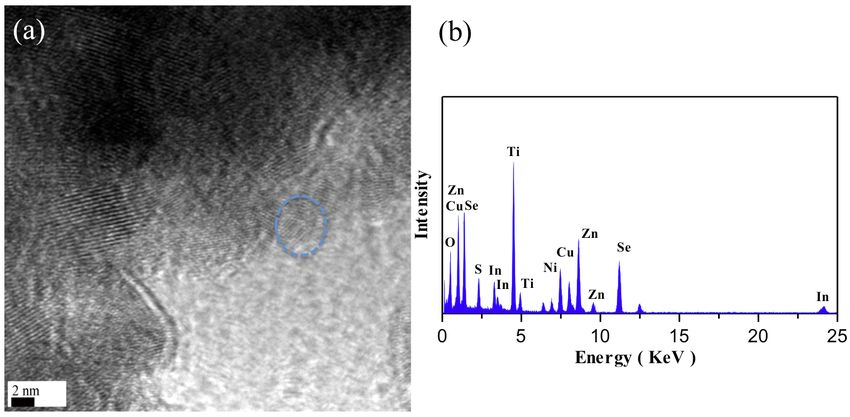
Fig. S8. (a) TEM images of Cu2S/CuInS2(6)/ZnSe(3) configurations prepared by
SILAR process. Blue square dots represent the QDs deopised on the TiO2
nanocrystals (b) EDX spectrum of Cu2S/CuInS2(6)/ZnSe(3) deopised on the TiO2
nanocrystals. The Ni peaks are due to the Ni TEM grid used in the measurement.Electronic Supplementary Material (ESI) for Chemical Communications
This journal is © The Royal Society of Chemistry 2012
Referneces
1. H. Lee, M. Wang, P. Chan, D. R. Gamelin, S. M. Zakeeruddin, M. Gratzel and M.
K. Nazeeruddin, Nano. Lett., 2009, 9, 4221.
2. S. Li, Z. Zhao, Q. Liu, L. Huang, G. Wang, D. Pan, H. Zhang and X. He, Inorg.
Chem., 2011, 50, 11958.
3. L. D. Partain, R. A. Schneider, L. F. Donaghey, P. S. Mcleod, J. Appl. Phys., 1985,
57, 5056.
4. Q. Guo, S. J. Kim, M. Kar, W. N. Shafarman, R. W. Birkmire, E. A. Stach, R.
Agrawal and H. W. Hillhouse, Nano Lett., 2008, 8, 2982.
5. M. -Y. Chiang, S -H. Chang, C. -Y. Chen, F. -W. Yuan and H. -Y. Tuan, J. Phys.
Chem. C., 2011, 115, 1592.
6. P. Cacciafesta, K. R. Hallam, A. C. Watkinson, G. C. Allen, M. J. Miles and K, D.
Jandt, Surf. Sci., 2001, 491, 405.You can also read