Enabling the 5G RF front-end module evolution with the DSMBGA package
←
→
Page content transcription
If your browser does not render page correctly, please read the page content below
Enabling the 5G RF front-end module evolution with the
DSMBGA package
By Curtis Zwenger [Amkor Technology, Inc.]

W                ith the r ise of 5G
                 w i r ele s s t e ch nolog y,
                 cellular frequency bands
have increased considerably, requiring
                                                 frequencies greater than 24GHz provides
                                                 opportunities for the adoption of new
                                                 packaging architectures and platforms.
                                                 An example is the integration of the
                                                                                                           For 5G, small cells are low-powered
                                                                                                        cellular radio access nodes that operate
                                                                                                        in licensed and unlicensed spectrums
                                                                                                        that have a range of 10 meters to a few
innovative solutions for the packaging of        antenna into the package. To do this,                  kilometers. Small cells are critical to 5G
radio frequency (RF) front-end (RFFE)            major design changes and new low-loss                  networks because 5G radio waves cannot
modules for smar t phones and other              materials are required.                                travel long distances due to 5G’s higher
5G-enabled devices. Our double-sided                 5G technology enables advancements                 frequencies [1].
molded ball grid array (DSMBGA) is               in products in all the major integrated                   In a technique called beamforming, the
an example of such solutions. Double-            circuit (IC) market segments,                          base station computer will continuously
sided packaging technology has vastly            i n cl u d i n g : 1) Mo b i l it y ; 2) IoT; 3)       calculate the best route for radio waves to
increased the level of integration for RF        Automotive (advanced driver assistance                 reach each wireless device and organize
front-end modules used in smartphones            systems (ADAS)); 4) High-performance                   mult iple anten nas to work together
and other mobile devices. Common RF              computing (HPC)/networking; and 5)                     as phased ar rays to create beams of
front-end modules consist of a low noise         5G net work topologies. 5G is more                     millimeter waves to reach the device [2].
amplifier (LNA), power amplifier (PA),           than a new generation of technologies.                    Edge computing occurs by locating servers
an RF switch, RF filters and duplexers.           It denotes a new era in which                          closer to the ultimate user. This distributed
   Advanced system in package (SiP)              connectivity will become increasingly                  computing reduces latency and data traffic
design rules and DSMBGA technology               f luid and f lexible. 5G networks will                 congestion. For the 5G ecosystem, cloud
enable the integ ration of additional            adapt to applications and performance                  data centers provide the computing core.
components – such as antenna tuners              and will be tailored precisely to the                  Figure 1 shows the architecture of these
and passive components – freeing up              needs of the user.                                     mmWave-enabled changes.
premium device motherboard real estate.

5G overview
   5G is the fifth-generation technology
standard that cellular phone companies
began deploying worldwide in 2019. It
includes three distinct classifications as
noted below.
   Low-band 5G Internet of Things
( IoT ). Low-band 5G uses a si m ilar
frequency range to 4G cellphones, 600–
850MHz, delivering download speeds
a little higher than 4G: 30–250Mbps.
Low-band cell towers have a range and
coverage area similar to 4G towers. In
this range, packaging can be similar.
   Mid-band 5G sub-6. Mid-band 5G
sub-6 is an upgrade of 4G technology
and involves incremental innovation
in packaging. Operating at frequencies
below 6GHz, the minor modifications
of current RF packaging architectures
result in minimal changes to the bill of
materials (BOM).
   5G mi l l imeter Wave (mmWave).
5G mmWave technology is a disruptive
innovation. The introduction of mmWave           Figure 1: Small cells connected by beamforming technology link to data centers in 5G-enabled
                                                 communications.

                                                        Reprint from Chip Scale Review September • October • 2021 [ChipScaleReview.com]            1
Outlook on 5G market growth                                   Fur ther reduction of package size                     using SiP methodolog y enables
   By 2025, 5G net work s a re li kely                    and losses requires close proximit y                       cu stome r s to desig n , t u ne a nd t est
t o c ove r o n e - t h i r d of t h e wo r l d’s         of t he t r a n sceive r a nd f ront- end                  R F sub -systems, allowi ng for a
population. The impact on the mobile                      module. Package-level integration of                       r e d u c t ion i n d e sig n it e r at ion s a nd
i ndu st r y a nd it s cu stome r s w ill be              antennas or antenna in package (AiP)                       an accelerated time-to-market.
profou nd [1]. I n addit ion, by 2026,                    designs within the RF module as well                           Advanced SiP package integration is
5G will have more tha n 3.5 billion                       a s si mu lt a n e o u s m o d el i n g of h e a t         being utilized for 5G packaging for a
subscriptions and will grow faster than                   dissipation to keep active components                      myriad of reasons [7]:
4G in most regions, per the Ericsson                      wit h i n accept able t her mal li m its
Mobility Report, June 2021 [3].                           address these needs. The integration of                      • More f lexibilit y for system
   The advanced packaging market for                      power amplifiers with antenna arrays                           d e sig n e r s – t o m i x a n d m a t c h
5G RFFEM is projected to reach US$2.3                     to address the design issues of size,                          IC technologies, optimize
billion by 2026, representing a 30%                       cost and performance is a critical step.                       perfor mance of each f u nctional
compound annual growth rate (CAGR)                        For package desig ners, the solution                           block and reduce cost.
according to Yole Développement (Yole),                   to these challenges incor porates                            • Faster time to market (compared
SA, an industry consulting fi rm [4].                      mu lt i-l aye r f a b r ic a t io n w it h f i n e -           t o t h e s y s t e m o n c h i p (S o C )
   “There has been a change in                            l i ne fe at u re s a nd pre cise laye r-t o -                 approach).
f requencies with the ar r ival of 5G,                    layer registration, advanced low-loss                        • Reduced motherboard complexity
adding frequency bands above 3GHz                         materials to reduce conductive losses                          – by m ig r a t i n g sig n a l r o u t i n g
i n F R 1 , a n d m mW a v e i n F R 2 , ”                and co-simulation of circuit, device,                          complexity to the package
according to A ntoine Bon nabel,                          package and thermal performance.                               substrate.
Tech nolog y & Ma rket A nalyst, R F                          T he t r a n sit ion t o 3D pa ck age                    • Better performance – various ICs
Devices and Technology at Yole [5].                       i nt eg r at ion at h ig he r p owe r level s                  and passives placed close together
“ T h i s a n d t h e s y s t e m - l e ve l t r e n d    and frequencies requires exceptional                           means shorter line length, which
have had a profound impact on both                        isolation between the various circuit                          reduces resistor (R), inductor (L)
t he nu mber of component s a nd t he                     blocks. In addition, for high-volume                           and capacitor (C) losses leading to
technology platfor ms on which they                       deployment, the manufacturing costs                            higher signal integrity and lower
are built.”                                               of high-power amplif iers and large                            power consumption.
                                                          a nt e n na a r r ays i n m il l ion s of ba se              • Lower system cost – compared to
RF front-end integration history                          stations must be addressed [6].                                discrete packages, optimized SiP
   The next sections discuss the                              5G R F packaging technology                                solutions result in overall system
challenges associated with 5G packaging                   t o o l b o x . To m e e t t h e t e c h n i c a l             cost reduction.
along with the associated “toolbox”                       demands for complex 5G R F f ront-                           • Small for m factor – sub-system
available to enable solutions.                            end modules, advanced package                                  si z e i s r e d u c e d by i nt eg r a t i ng
   5G IC packaging challenges. Advanced                   integration techniques must be                                 multiple dies and passives into a
packaging for 5G systems requires the                     deployed. An advanced SiP technology                           single SiP.
integration of RF, analog, and digital                    t o olb ox a d d r e s s e s t he s e d e m a nd s.          • Improved reliability – better solder
functions along with passives and other                   Figure 2 identifies the key attributes                         joi nt c on ne c t ion s c ompa r e d t o
system components into a single module.                   of an effective 5G technology toolbox.                         discrete components assembled
Called heterogeneous integration (HI), the                    The g rowing nu mber of new                                on a board/printed circuit board
advanced SiP designs that accomplish this                 f requencies, combined with the                                (PCB) result because the SiPs are
integration become more important for 5G                  v a r i e t y of m u l t i p l e x i n g m e t h o d s ,       molded, which alleviates stress in
because of several reasons, including:                    significantly increases the complexity                         the joints.
                                                          of t he R F f ront- e nd. I nt eg r at ion
    a) I n t e g r a t i o n of a n t e n n a s w i t h
       transceiver ICs and other circuitry;
    b) Addition of the sub-6GHz frequency
       range 1 (FR1) in the near-ter m
       through advances in packaging
       technologies;
    c) New mmWave bands frequency
       range 2 (FR2) drive the integration
       of RF circuitry, including filters,
       d iplexer s, broa dba nd power
       amplifiers and switches; and
    d) The add-on modules to the
       existing RFFE require optimum
       miniaturization and component
       integration.
                                                          Figure 2: An advanced RF packaging technology toolbox incorporates many different tools.

2       Reprint from Chip Scale Review September • October • 2021 [ChipScaleReview.com]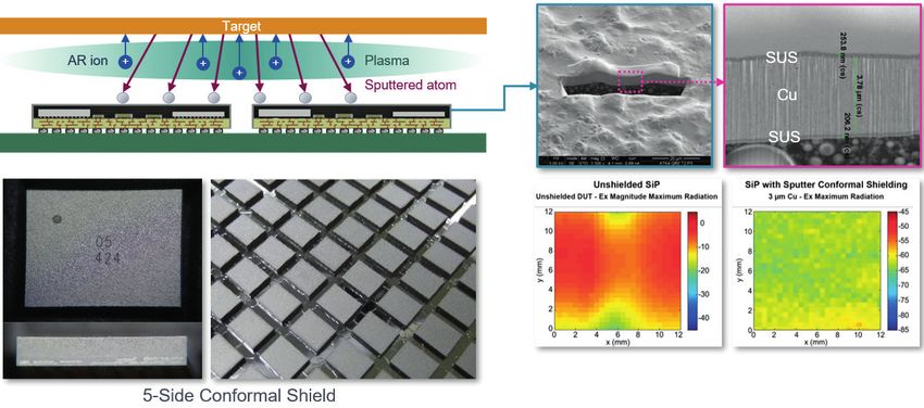
Figure 3: Integrated FEMiD and PA in the cellular handset PAMiD. IMAGE SOURCE: Yole Développement SA.
Figure 5: Typical SiP design rule attributes.
a nd must be opt i m i zed for h ig h-
volu me manufact u r i ng. Molded
u nder f ill (M U F) is com monly used
to reduce process cost and decrease
package spaci ng requ i rement s. For
a robust M U F process, the molding
t e c h n i q u e (e . g . , c o m p r e s s i o n v s .
t ransfer molding), the mold process
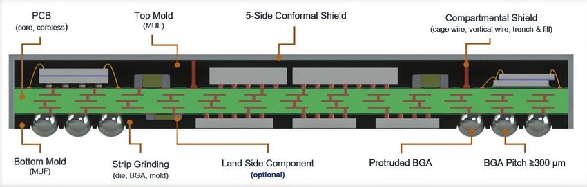
Figure 4: DSMBGA enabling technologies include both top and bottom molded underfill. p a r a m e t e r s (e . g . , t r a n s f e r t i m e ,
pressure, temperature) and the mold
The introduction of DSMBGA robu st a nd cost- ef fect ive a ssembly compound material must be carefully
To m e e t t h e h i g h l e v e l s o f technology. Figure 4 illustrates the cho s e n a nd o pt i m i z e d t o e n s u r e a
i nt eg r at ion r e q u i r e d for 5G f r ont- e x t e n sive t e c h n olog ie s a p pl ie d t o h ig h -y ield i ng p r o d u c t io n p r o c e s s .
end modules, an extension of existing c r e a t e t h i s R F f r o n t- e n d p a c k a g e Subst rate solder mask t h ick ness
single-sided SiP package technologies w i t h k e y p e r fo r m a n c e a t t r i b u t e s . cont rol a nd st r ateg ically located
w a s p u r s u e d . T h e c o m bi n a t io n of With additional power amplif ication solder ma sk kee p - out zones help
s eve r a l e n a bl i ng p a ck a ge fe at u r e s and filtering circuitry, the DSMBGA ensure the molded underfill’s process
and assembly processes resulted i n p a ck a ge i mp r ove s sig n a l i nt eg r it y quality and the package’s long-ter m
t he dou ble - sid e d mold e d ba l l g r id and reduces losses, resulting in reliability are as robust as possible.
ar ray (DSMBGA) package. Package i m p r ove d R x / Tx a m pl i f i c a t i o n , Advanced design rules are
d e v e l o p m e n t b e g a n i n 2 018 a n d which translates into reduced system rigorously validated through extensive
the f i rst product was released to power requirements. process optimization, work manship
product ion i n May 2020. Fig ure analysis and component/ board-level
3 shows a t y pical block d iag ra m Advanced SiP design rules reliability testing. Figure 6 represents
of a DSM BGA f ront- e nd modu le A c r it ical be nch m a rk for a ny IC a t y pical advanced SiP test vehicle
w it h i nt eg r at e d duplexe r ( F EM i D) package technology is its design rules. (T V ) that cont ai ns var ious sized
and a power amplif ier module with Fo r DSM BGA , t he mo s t a d va n c e d
integrated duplexer (PAMiD). SiP design rules are applied to enable
To p r o v i d e t h e h i g h l e v e l o f a highly i nteg rated and small for m
i nteg rat ion noted above, several factor package. Figure 5 illustrates
enabling technologies were combined the typical SiP design rule attributes
to create a DSMBGA f ront-end fo r p a c k a g e m i n i a t u r i z a t i o n . T h e
module. By utilizing strip grinding, minimum spacing for packages and
molded underf ill (MUF) and components is directly related to the
double -sided mold i ng, combi ned substrate supplier’s process capability
with indust r y-leading desig n r ules, (e.g., for solde r ma sk reg ist r at ion)
significant advancements in package coupled with the package/component
size reduction were achieved. Other physical tolerances, assembly
i mprovements i nclude st ate - of-the - process robust ness a nd assembly
a r t c o n fo r m a l a n d c o m p a r t m e nt a l m a t e r i a l s u s e d . Fo r e x a m ple , t o
shielding for electromagnetic prevent component tombston i ng,
i nter ference ( EM I ) isolat ion a nd t h e s u b s t r a t e b o n d p a d g e o m e t r y,
at tenuation and implementation solder paste stencil desig n and
of i n-li ne R F test i ng to deliver Figure 6: Example of an advanced SiP design rule
s ol d e r p a s t e m a t e r i a l a l l i n t e r a c t validation test vehicle.
Reprint from Chip Scale Review September • October • 2021 [ChipScaleReview.com] 3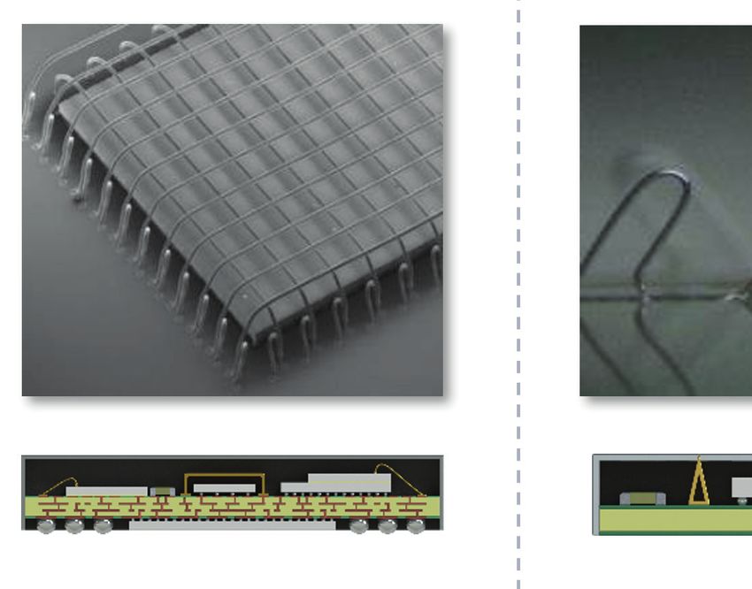
f lip-chip chip-scale packages (CSPs)
and passive components. Solder
mask-def ined and non-solder mask-
def ined bond pads are incor porated
i nt o t h e T V t o va l id a t e t h e ef fe c t
o n c o m p o n e n t / p a c k a g e s t a n d - of f ,
tombstoning and MUF performance.
T he a ssembled test veh icle is t hen
subje ct e d t o t he t y pical bat t e r y of
c o m p o n e n t- l e ve l r e l i a b i l i t y t e s t s ,
including high-temperat u re storage
(HTS), preconditioning, temperature
cycl i ng ( TC), a nd u nbia se d h ig h ly
a c c e l e r a t e d s t r e s s t e s t (u H A S T ) .
Board-level reliability is also verified
through temperature cycling and drop
shock testing.

EMI shielding
    Maintaining signal integrity
within the DSMBGA package
wa s e s se nt ia l t o g u a r a nt e e syst e m
p e r f o r m a n c e . To m i n i m i z e a n y                Figure 7: EMI/RFI shielding techniques minimize electrical disturbances in and near the package.
electrical disturbances and resulting
sig nal deg radation i n an IC and its                          a conformal shield can be applied to                      electrically conductive wall to create
s u r r o u n d i n g c i r c u it r y, i n n ov a t ive        select areas of the package, if needed.                   the EMI shield par titioning needed.
ele ct romag net ic i nt e r fe re nce/r a d io                 Compar tmental shielding is another                       More advanced compar tmental
f r e que ncy i nt e r fe r e nce ( EM I / R F I )              EMI suppression technology utilized                       shielding tech niques have been
shielding needed to be integrated in                            i n t he DSM BA package. T hese                           developed that utilize sophisticated
t he st r uct u re. F i g u re 7 i l lu st r at e s             compar tmental shielding techniques                       w i re bond tech nolog ies to create a
some of the EMI shielding techniques                            showcase ad apt able desig ns for                         wire fence, a wire cage or a vertical
that have been incor porated into the                           i nt e r n a l c o m p o n e nt- t o - c o m p o n e nt   w i r e s t r u c t u r e w i t h i n t h e m ol d e d
DSMBGA package.                                                 shielding with in-package partitioning.                   package. Strip grind or laser ablation
    B y l e ve r a g i n g i n d u s t r y- l e a d i n g          The original compar tmental                            processes a re used to reveal t he
physical vapor deposition (PVD) tools,                          sh ield i ng t e ch n ique wa s k now n a s               encased wire. Conformal shielding is
a thin metal stack-up is applied to the                         t rench a nd f ill. Laser ablat ion was                   then applied to create a Faraday cage
external surfaces of the package and                            u se d t o c r e at e a t r e nch w it h i n t he         ef fe ct , whe reby t he w i re st r uct u re
coupled to an exposed ground plane in                           m ol d c o m p o u n d t o r e ve a l g r o u n d         se r ve s t o blo ck ele ct r ic f ield s a nd
the DSMBGA’s organic substrate. This                            connections on the underlying                             ele c t r o m a g n e t ic w ave s [8]. T h e s e
conductive EMI coating is referred to                           subst rate. A conduct ive epoxy was                       EMI shielding str uct ures are shown
as conformal shielding. By applying                             dispensed i n t he t rench to for m a n                   in Figure 8.
state-of-the-ar t masking techniques,

Figure 8: EMI shielding techniques for DSMBGA packages to achieve improved system performance.

4       Reprint from Chip Scale Review September • October • 2021 [ChipScaleReview.com]
Figure 9: Conformal shielding and EMI radiation suppression effectiveness.
The conformal shielding technology coat i ng to ensu re ef fect ive EM I majority of DSMBGA packages being
r e q u i r e s s t r i c t c o n t r ol s t o e n s u r e shielding. Figure 9 also compares the used today are for PAMiD products.
process quality and yield. To enable EMI shielding effectiveness between H i s t o r i c a l l y, t h e s e p r o d u c t s we r e
this capability, PVD was adapted to an unshielded and a shielded package. ser ved by si ngle -sided Si P desig ns
p a c k a g e -l e vel p r o c e s s i n g. F i g u r e because the front-end module circuit
9 illust rates t he PV D con for mal 5G front-end module evolution and complexity was not ver y demanding
sh ieldi ng tech n ique. A focused ion roadmap (e.g., for 3G applications).
bea m ( FI B) cut is u sed to valid ate Vir tually any 5G R F system W i t h t h e a d v e n t o f 4 G LT E ,
t h e m e t a l s t a c k t h i c k n e s s . Fo r a ci rcu it r y ne e d i ng comp one nt-level medium- and high-band power
5 -sided appl icat ion , t he PV D mu st integ ration can benef it f rom the amplif ication and f ilter ing circuit y
be optimized to get accu rate and size, cost and perfor mance benef its became more demanding with up to
repeatable top su rface and sidewall offered by the DSMBGA package. The f ive R F f ront-end modules required
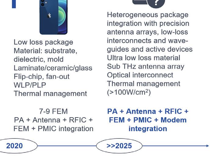
Figure 10: Packaging integration evolution and trends in smartphones. SOURCE: [9]
Reprint from Chip Scale Review September • October • 2021 [ChipScaleReview.com] 5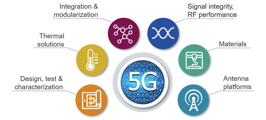
a b o u t 5 G ,” I E E E S p e c t r u m
                                                                                                                     magazine, Jan. 27, 2017, Institute
                                                                                                                     of Elect r ical a nd Elect ron ic
                                                                                                                     Engineers.
                                                                                                                3.   “Ericsson Mobility Report, June
                                                                                                                     2021,” https://www.ericsson.com/
                                                                                                                     en /mobility-repor t/repor ts/june-
                                                                                                                     2021, Ericsson.
                                                                                                                4.   “5G Pa ck a g i ng Tr e nd s for
                                                                                                                     Smartphones 2021,” www.yole.fr,
                                                                                                                     Yole Développement SA, 2021.
Figure 11: Example of a PAMiD DSMBGA product showing layout a) (left) before MUF; b) (middle) top; and c)
(right) bottom after MUF and EMI shielding.                                                                     5.   “Cellular RF Front-End
                                                                                                                     Technologies for Mobile Handset
in a single handset. This led to the                     r u les for 3D compone nt pla cement                        2 0 2 1 , ” w w w.y o l e . f r , Yo l e
evolution of DSMBGA’s predecessor,                       and double-sided molding, together                          Développement SA, 2021.
t h e D S B G A (d o u b l e - s i d e d B G A)          with confor mal and compar t ment al                   6.   A. O. Wat a nabe, M. A li, Sk Y.
p a c k a g e w h e r e IC s we r e m o u n t e d        shieldi ng and i n-li ne R F testi ng,                      B. Sayeed, R. R. Tummala, P. M.
to the bottom of the str uct ure. This                   delivers integration levels in a small                      Raj, “A review of 5G f ront- end
allowed for sig nif icant module                         form factor with high yield.                                systems package,” I EEE Trans.
si ze reduct ion for t he equ ivalent                       I n addition to for midable Si P                         on Components, Packaging and
circuit r y in a single-sided SiP                        capacity and DSMBGA technology, an                          Ma nufact u r i ng Tech. ( Vol.: 11,
st r uct u re. T hen, with the evolution                 extensive toolset has been developed                        Issue: 1, Jan. 2021).
of the 5G cellular spect r u m, f ront-                  to ma x i m i ze per for ma nce a nd to                7.   “System-in-Package Technology
end module complexit y f u r ther                        address the sophisticated packaging                         and Market Trends 2020,” www.
i nc re a se d w it h t he i nt roduct ion of            for mat s re qu i re d t o product i ze 5G                  yole.fr, Yole Développement SA,
ultra-wideband (UWB) circuitry.                          a p pl ic a t io n s . S o m e of t h e s e t o ol s        2020.
    To suppor t t hese mult iple ba nd s,                include AiP, substrate-embedded die,                   8.   S . J. C h a p m a n , D. P. H e we t t ,
up to seven and nine f ront-end                          wafer-level SiP and a variet y of R F                       L . N. Trefet he n , “ Mat hemat ics
modules were requi red for 5G sub -                      shielding design options. This toolset,                     of t h e Fa r a d ay C a ge ,” ht t p s: //
6GHz and 5G mmWave applications,                         combined with expertise in RF module                        people.maths.ox.ac.uk /trefethen/
r e s p e c t ivel y. T h i s r e s u lt e d i n t h e   desig n, cha racter i zat ion a nd bench                    chapman _ hewet t _t refethen.pdf,
advent of the DSMBGA package. The                        test, enables us to ser ve customers                        SIAM Review, Vol. 57, No. 3, pp.
latest version of the DSMBGA package                     who want to outsource the challenges                        398-417.
is almost 50% smaller than the f irst                    (including the substantial investment)                 9.   “5G Pa ck a g i ng Tr e nd s for
m id-/ h ig h-ba nd PA Mi D. T ha n k s to               associated with combining multiple                          Smartphones 2021,” www.yole.fr,
in novations such as EMI shielding,                      ICs with advanced package assembly                          Yole Développement SA, 2021.
f lip-chip PA and double-sided molded                    and test technologies for 5G networks.
BGA pa ck ag i ng, PA M i D s up pl ie r s                  As demand for packages that support
managed to integrate the same system                     5G cl i m b s , we a r e wel l u n d e r w ay
in a smaller footprint [9]. Figure 10                    with the successful implementation of
illustrates the evolution and roadmap                    DSMBGA technology having been in
for R F front-end module integration                     production for high-volume markets
for 5G smartphones. Figure 11 shows                      for more than a year.
an example 5G PAMiD product in a
DSMBGA package.                                          References
                                                           1. “5G Global Launches & Statistics,”
Summary                                                       https://www.gsma.com/futurenetworks/
  T h e a d v a n c e d Si P d o u bl e - s i d e d           ip _services/understanding-5g/5g-
molded BGA platform has become an                             innovation/, GSMA.
industry technology standard in this                       2. A . N o r d r u m , K . C l a r k ,
domain. Applying leading-edge design                          “Eve r y t h i ng you need to k now

                        Biography
                          Curtis Zwenger is VP, Advanced SiP Product Development, at Amkor Technology, Inc., Tempe, AZ. He
                        has held leadership roles in developing Amkor’s fine-pitch copper pillar, through-mold via and wafer-level
                        packaging technologies. He is currently responsible for advanced SiP, MEMS/sensor and memory product
                        development. He has been issued 30 U.S. patents and holds a degree in Mechanical Engineering from Colorado
                        State U. and an MBA from the U. of Phoenix. Email curtis.zwenger@amkor.com

6      Reprint from Chip Scale Review September • October • 2021 [ChipScaleReview.com]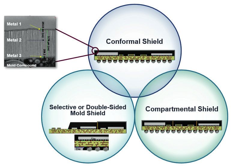
You can also read