ENABLING THIN GLASS SOLUTIONS FOR 5G - INEMI
←
→
Page content transcription
If your browser does not render page correctly, please read the page content below
ENABLING THIN GLASS SOLUTIONS FOR 5G
Aric Shorey
VP Business Development Mosaic Microsystems
Co-Authors
David Levy / Shelby Nelson / Paul Paul Ballentine

Webinar recording (note: due to technical difficulties, the recording starts on slide 3)
YouTube: https://youtu.be/TlrTSXQ5_xg
Alternate link: http://thor.inemi.org/webdownload/2021/5G-mmWave_Enabling_Thin_Glass.mp4

 July 15, 2021
Outline/Agenda

• Motivation
• Advantages of glass packaging solutions
• Handling challenges
• Solutions to enable volume manufacture
• Examples showing advantages of glass based devices
• Summary
• Q &A

 1
 Mosaic Microsystems
Thin glass addresses industry needs

 New material solutions are needed to
 address needs in RF communications
 • Low loss for 5G/mmWave
 • Military
 • Reduced footprint

 Advanced packaging solutions are
 needed to extend industry performance
 targets
 • Interposer
 • Embedded die
 • Hermetic

 2
 Mosaic Microsystems
Material properties of glass provide attractive solutions Good
 Fair
 Poor

 Materials
 Characteristic Ideal property
 Glass Si Organic Ceramic
 • High resistivity
 Electrical
 • Loss loss, low k
 • Smooth surface
 ✓ Low loss Physical • Large area scalability
 • Ultra thin
 ✓ CTE match
 Thermal • High conductivity
 ✓ Smooth • High strength, modulus
 Mechanical
 • Low warpage
 ✓ Thin • Resistance to process
 Chemical
 chemistry
 ✓ Cost-effective
 Via and RDL cost • Low cost for both
 ✓ Scalable
 Reliability • CTE match to Si and PWB
 Cost/mm 2 • @25 um I/O pitch
 Based on chart from Georgia Tech PRC

 3
 Mosaic Microsystems

Handling glass < 200 um thick has challenges

 Challenges for TGV in thin glass

 • Handling thin glass in semiconductor fab environment
 • Metallizing vias in a reliable, cost-effective way

 4
 Mosaic Microsystems
New approach to enable thin glass

 New approach:
 Thin glass with through-holes temporarily bonded to silicon
 handle wafer using Viaffirm™ technology

 • Addresses flatness
 • Equipment interface is Si wafer
 • Provides path to existing metallization processes

 Can be processed like a standard silicon wafer
 5
 Mosaic Microsystems

Robust temporary bonding
 • New process relying on a thin inorganic layer
 Via formation
 Bond
 • Very resistant to temperature, harsh
 chemistries
 • No outgassing
 Process
Adhesive on handle • Thin adhesion layer → Excellent flatness
 • Debond:
 Debond – Simple, mechanical
 – Adhesion layer stays on handle
 • Compatible with silicon processing
 (installed equipment base)

 6
 Mosaic Microsystems
Key aspects of Viaffirm™ technology

 • Bond is temporary to ≥400⁰ C • Mechanical de-bond with
 •
Debond process

• Mechanical de-bond with low force
• Demonstrated with commercial volume tools (Suss, CEE)

• Debond residue on device wafer?
 –XPS measurement pre/post bond
 –Carbon differences likely adventitious
 –Low impact on glass peaks:
Process scalability
 Demonstrated to 300 mm diameter (and beyond)

 100 mm 150 mm 200 mm 300 mm

 9
 Mosaic Microsystems
Mosaic Process Flow – Via fill
 Leverage established processes for metallized TGV

 a) d)

 b)

 e)

 c)

 f)

 Mosaic Microsystems
Via Fill on Mosaic bonded pair

 After plating
 • ~30 um via / 100 um glass on silicon handle

 • MOCVD Seed layer / Cu plate
 – Void free via fill
 Via fill
 • CMP:
 – Bond energy sufficient: no issues

 • Post-CMP anneal (400 ºC)
 – No cracking at vias
 After CMP

 After anneal

 11
 Mosaic Microsystems
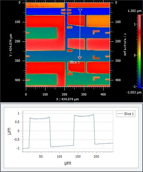
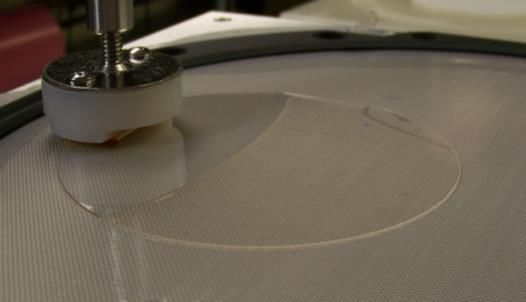
TGV Planarity
 Back side TGV planarity < 100 nm at de-bond

a) De-bond glass wafer and inspect via planarity after
 de-bond • Measure roughness/planarity with white light
 • No post-debond CMP interferometer (Zygo ZeGage™)
b) Top view of via after debond • Vias planar to < 100 nm

 7/19/2021 Mosaic Microsystems
 12
Hermeticity • Sample Description: – 35 m via in HPFS / Temporary bond to HPFS handle He leak test regions: – Cu plate bottom up via fill 35mm diameter – CMP to remove ~4 m overburden ~3300 vias each – Mechanical debond • Hermeticity assessment by helium leak test • Results 260C anneal – 8 of 9 regions at better than 1x10⁻⁹ atm-cc/s (detection limit) – After 260 °C anneal: • Leak performance still at 1x10⁻⁹ atm-cc/s and below as debonded • Slight change in via profile but remains at < 0.5 um deviation 13 Mosaic Microsystems
Use Cases

7/19/2021 Mosaic Microsystems
 14
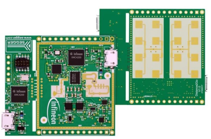
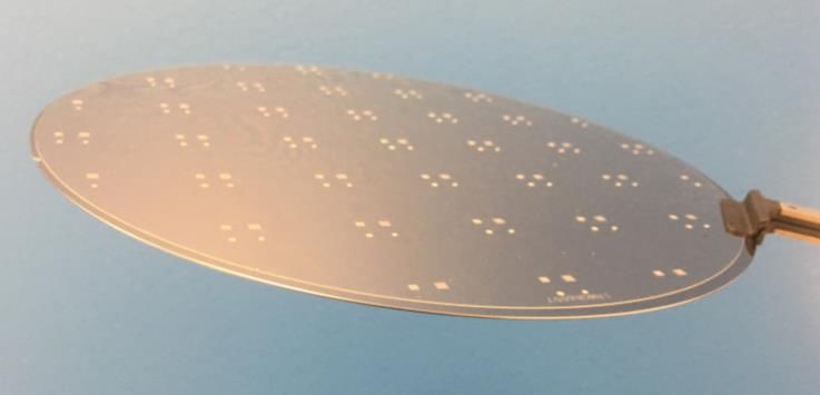
100x0.1 mm wafer – Plated and de-bonded
 All wafers yielded
 Thin glass supported by Reverse side of wafer,
 Metallized wafer on Si dicing tape after debond shown on dicing tape frame

 15
 Mosaic Microsystems
mmW packaging in glass

Wafers processed by
GE Research
Contact: Todd Miller
(millert@ge.com)

 2-layer RF interposer cross section 2-layer RF interposer under test

 • 0.15 mm thick glass
 • Thermal compression bond Au
 • Analysis shows glass based approach can provide 50% lower loss with standard
 glass. More than 70% with fused silica
 • In some applications you can realize >7x reduce package size volume (e.g. filters)
 • Primary impact from roughness/skin effect, which is pronounced in these relatively
 designs that can have conductor lengths as long as 50 mm
 • Demonstrators to be built in 2021

 16
 Mosaic Microsystems
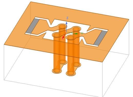
Thin glass solutions for 5G – 28 GHz
 Collaboration Between Mosaic and Fraunhofer IZM
 • Goals:
 – Characterize thin glass technology (BCB on fused silica glass) for mm-Wave 5G
 applications at 28 GHz
 – Design, fabrication and test of 2x2 aperture-coupled patch antenna arrays on thin
 glass for femtocells (10m-20m range)
 – Comparison between glass-based antennas and equivalent organic material-based
 solutions

 Investigated thin glass stack-up Investigated organic stack-up
 and material information and material information

 17
 Mosaic Microsystems
2x2 Aperture-Coupled Patch-Antenna Array – Geometry & Impedance
Matching

 Parameter Glass Organic
 x 2505 3710 2505 x 3710
 Port 5400 5400
 15.4mm 15.4mm
 Simulated antenna array geometry

 Simulated 3D antenna
 model

 Glass
 Organic Material -10dB
 Bandwidth
 Glass 1630MHz
 Organic 1670MHz

 Top view
 Simulated antenna array impedance
 matching

 18
 Mosaic Microsystems
2x2 Aperture-Coupled Patch-Antenna Array – Radiation
Pattern and Efficiency

 Material Peak realized Radiation effieciency
 Gain
 Glass Glass 10.9dBi@28 GHz 80%@28 GHz
 Organic
 Organic 10.5dBi@28 GHz 75.9%@28 GHz

 Simulated antenna array peak gain

 Conclusion:
 • Thin glass antenna array exhibits higher simulated peak gain and efficiency at 28 GHz and more
 stable maximum gain over the matched frequency band

 Next steps:
 • Fabrication of glass and organic material antenna arrays
 • Validation of simulation by means of antenna matching and radiation pattern measurement

 19
 Mosaic Microsystems
Metaconductor for low loss

How to decrease conductor loss?
 • Challenge: Frequency↑, Skin depth ↓, conductor loss ↑
 • Cu/Co metaconductor increases effective skin depth
 • Provides 50% resistance reduction at 28GHz

 Seahee Hwangbo, Arian Rahimi, and Yong-Kyu Yoon, “Cu/Co Multilayer based High Signal
 Integrity and Low RF Loss Conductors for 5G/Millimeter Wave Applications,” IEEE
 Transactions on Microwave Theory and Techniques, vol. 66, no. 8, August 2018, pp. 3773 –
 3780

 Mosaic Microsystems
Demonstrator: Fused silica integrated 3D inductor
 Simulations – Inductors with 2x Q-Factor
 1) 1 turn inductor 2) 2 turn inductor

 Cu
 150nm
 Co
 25nm

 300μm
 10 pairs of Cu/Co
 Q factor metaconductor Q factor
 130% improvement 108% improvement
 =

 : frequency
 L: inductance
 R: resistance
 21

 Mosaic Microsystems
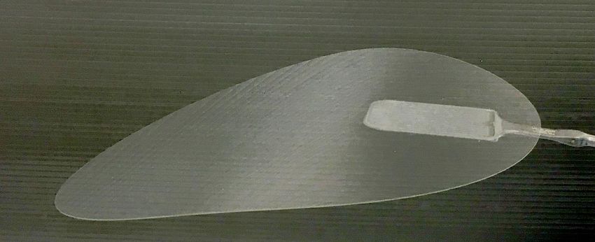
Targeted application is to integrate metaconductor into radar array
 Expect broad application of the technology
• Fabricated antenna will be integrated with 24 GHz transceiver module

1) 2D Array 2) 3D Array – 2 layer
 with TGV feed
 Tx/Rx
 components will
 be replaced by the
 proposed antenna

 24 GHz transceiver module1

 4. https://www.infineon.com/cms/en/product/evaluation-boards/demo-distance2go/

 Mosaic Microsystems
Opportunities for embedded die
 Viaffirm well-suited to make novel, hermetic devices

 • Die level He leak performance has been demonstrated to < 1e-8 atm-cc/s

 TGV wafer Cavity wafer TGV wafer

 < 300 um

 23
 Mosaic Microsystems
Summary
• Industry trends require new packaging solutions
• Viaffirm enables cost-effective manufacture for glass/TGV and other
 thin substrates in a high volume environment
• Several recent applications have demonstrated suitability to leverage
 existing processes for thin glass applications
• Broad potential application for RF filters/antenna, MEMS, packaging
 (interposers), hermetic designs, sensing etc.
• Unlocking the value of glass solutions
 – 2021 demonstrators for ESA, radar and heterogeneous integration

 24
 Mosaic Microsystems
Thank You!
 Aric Shorey
VP Business Development
 Mosaic Microsystems
www.mosaicmicro.com

aric.shorey@mosaicmicro.com
 (585)304-7163

 Mosaic Microsystems
Acknowledgments
➢ Support from AFWERX and the National Science Foundation
➢ Alan Huffman and Jennifer Ovental from Micross Components
➢ Catherine Bullock, Peter Wrschka and Lynn Shumway from Axus
 Technologies
➢ Todd Miller, Joe Iannotti, Chris Kapusta and Joleyn Brewer from
 General Electric (millert@ge.com)
➢ Marco Rossi, Thi Hyen Li, Ivan Ndip from Fraunhofer IZM
➢ YK Yoon, Hae-In Kim, Woosol Lee from University of Florida

 Mosaic Microsystems
You can also read