Epitaxial stabilization of thin films of the frustrated Ge-based spinels
←
→
Page content transcription
If your browser does not render page correctly, please read the page content below
Epitaxial stabilization of thin films of the frustrated Ge-based
                                                                                                    spinels

                                                                 Denis M. Vasiukov,1, ∗ Mikhail Kareev,1 Fangdi Wen,1 Liang Wu,1
                                                               Padraic Shafer,2 Elke Arenholz,2, 3 Xiaoran Liu,1 and Jak Chakhalian1
                                                                                  1
                                                                                      Department of Physics and Astronomy,
arXiv:1907.07785v3 [cond-mat.str-el] 22 Jun 2021

                                                                      Rutgers University, Piscataway, New Jersey 08854, USA
                                                   2
                                                       Advanced Light Source, Lawrence Berkeley National Laboratory, Berkeley, CA 94720, USA
                                                                              3
                                                                                  Cornell High Energy Synchrotron Source,
                                                                             Cornell University, Ithaca, NY 14853, USA
                                                                                              (Dated: June 23, 2021)

                                                                                                   Abstract
                                                        Frustrated magnets can host numerous exotic many-body quantum and topological phenomena.
                                                   GeNi2 O4 is a three dimensional S = 1 frustrated magnet with an unusual two-stage transition to
                                                   the two-dimensional antiferromagnetic ground state, while GeCu2 O4 is a high-pressure phase with a
                                                   strongly tetragonally elongated spinel structure and magnetic lattice formed by S = 1/2 CuO2 lin-
                                                   ear chains with frustrated interchain exchange interactions and exotic magnetic behavior. Here
                                                   we report on the first thin-film epitaxial stabilization of these two compounds. Developed growth
                                                   mode, surface morphology, crystal structure and copper valence state were characterized by in-situ
                                                   reflection high-energy electron diffraction, atomic force microscopy, X-ray reflectivity, X-ray diffrac-
                                                   tion, X-ray photoelectron spectroscopy and resonant X-ray absorption spectroscopy. Our results
                                                   pave an alternative route to the comprehensive investigation of the puzzling magnetic properties
                                                   of these compounds and exploration of novel emergent features driven by strain.

                                                                                                       1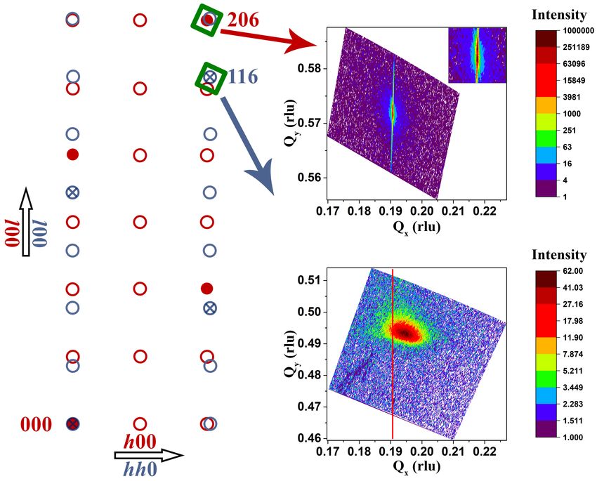
Research on magnetic systems possessing frustration, low dimensionality or their combi-
nation, is a very active and fruitful subfield with a great potential for emergent phenomena,
new states of matter and exotic excitations exemplified by spin ice, quantum spin liquids,
and spin-charge separation to name a few [1–4]. Despite a plethora of interesting theoreti-
cal proposals the mapping of theory to realistic material systems still remains a formidable
challenge, particularly, due to demand for high-quality materials that can host such exotic
phenomena and states [3, 5]. As one of the alternatives to the solid-state chemistry routes,
ultra-thin films may be a viable option to address the challenge.
   Among the magnetically frustrated materials, complex oxides with the spinel structure are
of special interest. Spinel oxides have the general formula AB2 O4 , composed of a cubic close-
packed sublattice of anions in which 1/8 of the tetrahedral (A-site) and 1/2 of the octahedral
(B-site) interstices are filled by cations. In the absence of distortions, spinel crystallizes in the
cubic space group F d3̄m and the B-site cations form a network of corner-shared tetrahedra
(also termed as “pyrochlore”) sublattice that can potentially trigger the strongest frustration
in three dimensions [6]. Following this direction, the so-called “4–2” spinel family with
germanium on the A-site is particularly interesting (general formula Ge4+ B2+
                                                                           2 O4 ), as this

class of compounds has magnetically inactive A-site; hence, their magnetic properties are
solely determined by the pyrochlore sublattice.
   In this work, we report on the first time epitaxially stabilized thin films of two members of
the “4–2” spinel family, GeNi2 O4 (GNO) and GeCu2 O4 (GCO), which exhibit very different
low-dimensional magnetic behavior. The bulk GNO undergoes a peculiar two-stage phase
transition in to a 2D magnetic ground state [7–12], while the bulk GCO shows a multiferroic
transition with interacting 1D S = 1/2 chains[13–16].
   In GNO the B-site Ni2+ has the 3d8 electronic configuration, which adopts a non-
degenerate electronic term 3 A2g with negligible single-ion anisotropy. The non-degeneracy
of Ni2+ indicates that frustration cannot be relieved via structural distortion driven by
the cooperative Jahn-Teller effect making this pyrochlore lattice of isotropic S = 1 spins,
shown in Fig. 1a, a promising candidate for unusual magnetic phenomena. Indeed, study of
NaCaNi2 F7 revealed continuum of quantum fluctuations characteristic for Coulomb phase
with only spin-glass-like freezing transition [18]. In contrast to this case, the unusual se-
quence of magnetic transitions is observed in bulk GNO at low temperatures leading to
antiferromagnetically ordered ground state with a propagation vector q = ( 21            1 1
                                                                                         2 2
                                                                                             )   corre-

                                                2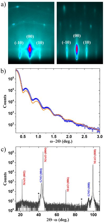
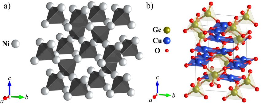
FIG. 1. Crystal structures of GeNi2 O4 and GeCu2 O4 spinels. a) In GNO the B-site sublattice of
Ni2+ ions form an ideal pyrochlore sublattice of corner-shared tetrahedra, the Ge and O ions are
omitted for clarity. b) The large tetragonal elongation in GCO results in the effective square-planar
coordination of Cu2+ ions therefore the B-site sublattice can be regarded as a set of alternating
mutually perpendicular layers of 1D chains. These structure figures were prepared using VESTA 3
software [17].

sponding to the rhombohedral lattice system [19]. Upon this transition the B-site splits
magnetically into alternating kagome and triangular planes along the (111) direction, which
form a set of intrinsically 2D frustrated sublattices.
   More detailed recent studies show that this antiferromagnetic state is developed through
two consecutive first-order phase transitions separated by ∼ 0.7 K (TN 1 = 12.1 K and
TN 2 = 11.4 K) without any measurable structural distortion [7–9, 20]. A subsequent muon-
spin relaxation experiment suggested that these two transitions correspond to distinct order-
ing of two magnetic subsystems [10]. Based on the single-crystal neutron elastic scattering
data [11] it was concluded that the first transition (TN 1 ) corresponds to a magnetic ordering
only within the kagome planes (each plane has ferromagnetic ordering stacked antiferromag-
netically) while the triangular planes become magnetically ordered at the second transition
(TN 2 ). Strikingly, the saturated magnetic moment of the triangular planes remains two times
smaller than one of the kagome planes [9, 11, 21], although in the absence of distortions all
Ni2+ ions are crystallographically equivalent. A strong magnetic anisotropy of the ground
state was demonstrated in the single-crystal experiments with applied magnetic field [21, 22].

                                                3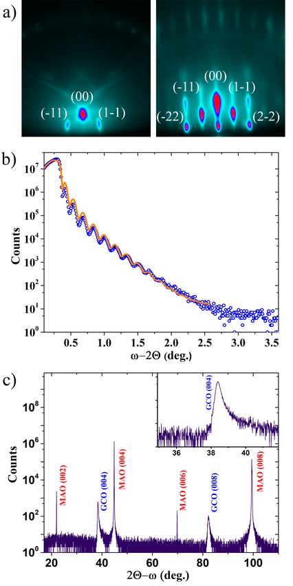
This highly unusual magnetic behavior seems to be closely related to the Gd2 Ti2 O7 with
pyrochlore structure which shows similar magnetic transitions [23].
   The specific-heat data indicate several puzzling features, which remain unexplained.
These include the presence of substantial magnetic correlations in the paramagnetic state de-
spite the low frustration factor (f = ΘCW /TN ∼ 0.7), the coexistence of gapped and gapless
spin waves, and missing of ∼ 40 % of the expected magnetic entropy [12]. Furthermore, un-
expectedly the change in magnetic entropy is almost equal for both phase transitions [8, 12],
which clearly contradicts to the picture of two separate orderings in kagome and triangular
planes (as triangular lattice contain three times less Ni2+ ions relative to the kagome lattice).
   As for the second synthesized spinel, GCO is a recoverable high-pressure phase with the
hausmannite structure type (space group I41 /amd). Interestingly, it is only the second
tertiary oxide discovered within the ternary Ge-Cu-O system [24] while the first one is the
celebrated GeCuO3 with 1D antiferromagnetic S = 1/2 chains, and the first discovered
spin-Peirls transition (i.e., spin pairing with a valence bond formation) among the inorganic
compounds [25]. GCO has a tetragonally distorted spinel structure in which the octahedral
B-site is occupied by the Cu2+ Jahn-Teller active ions. Due to the large Jahn-Teller distor-
tion, the local coordination of Cu2+ ions can be described as almost square-planar with the
in-plane Cu-O distance of 1.939 Å and the apical oxygens located at 2.504 Å [24]. As shown
in Fig. 1b, such a large distortion allows to consider this spinel structure as comprised of
alternating mutually perpendicular layers of 1D CuO2 S = 1/2 chains interconnected via
GeO4 tetrahedra. The 1D nature of magnetic interactions within the S = 1/2 chains is
supported by magnetic susceptibility data that show the characteristic Bonner-Fisher be-
havior with the ratio of inter-chain to intra-chain exchange couplings J 0 /J ∼ 0.16 [13]. The
susceptibility data also indicate the onset of long-range magnetic ordering at 33 K [13].
   Despite such a large tetragonal distortion of the pyrochlore sublattice, the magnetic in-
teraction between Cu ions in GeCu2 O4 remain frustrated in close analogy to the Cs2 CuCl4
case, where the frustrated interchain coupling results in the exotic “triplon” bound state
that readily moves between chains [26]. Theoretically, such an anisotropic pyrochlore lattice
was mapped onto a 2D crossed-chain model [27], which predicts the formation of a valence-
bond solid with a crossed-dimer state in the limit of small J 0 /J [27]. However, contrary
to the model calculations, the density-functional theory (DFT) study of GCO suggests the
formation of a spiral magnetic ground state [28]. The subsequent neutron powder diffrac-

                                              4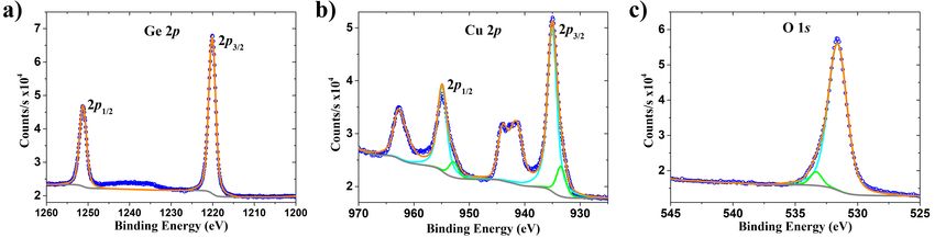
tion experiment revealed the presence of collinear antiferromagnetism at low temperatures
with an unexpected up-up-down-down (i.e. ↑↑↓↓) spin ordering pattern along the chains [14].
This unusual ordering pattern was attributed to the presence of bi-quadratic exchange inter-
action active in this compound [14] while a posteriori DFT study argued that actual reason
is the negligibly small nearest-neighbor coupling [29]. Surprisingly, two independent groups
recently reported spin-induced multiferroicity in GCO emerging at TN ∼ 33 K [15, 16],
which is incompatible with any theoretically proposed or experimentally determined mag-
netic structures [14, 27, 28]. To date, the nature of multiferroicity in GCO remains largely
unknown.
   Taking into account puzzling magnetism of these compounds and the fact that epitaxial
strain can alter the underlying microscopic Hamiltonian of a system, fabricating thin films of
GNO and GCO is of great interest since it can potentially shed light on the open questions
about the magnetic behavior of the bulk crystals and may lead to new emergent quantum
states. Moreover, in the bulk form GCO is only stable at high-pressure (∼ 4 GPa [24]) and
its high-pressure solid-state synthesis is difficult and yields only micron-sized single crystals
hindering application of many important probes. The epitaxial strain can help to stabilize
phases which are otherwise unstable at ambient pressure in the bulk [30], therefore exploring
the fabrication of GCO thin films can offer alternative opportunities for realizing large-area
single crystals.
   Here, we report on the first successful fabrication of GNO and GCO thin films by means
of pulsed laser deposition. The developed growth mode, surface morphology, film thickness
and crystal structure were characterized by in-situ reflection high-energy electron diffraction
(RHEED), atomic force microscopy (AFM), X-ray reflectivity (XRR) and X-ray diffraction
(XRD). Stoichiometry of the films and ion valency were investigated by X-ray photoelectron
spectroscopy (XPS). Electronic states in the GNO film were further studied by synchrotron
based resonant X-ray absorption spectroscopy (XAS) on Ni L-edge and O K-edge. The
combination of advanced tools confirms the successful epitaxial growth of high-quality (001)-
oriented GCO and GNO thin films.
   Stabilization of the GeNi2 O4 thin film. We begin with the description of details
of GNO growth. Taking into account that the bulk magnetic ground state in GNO has
q = ( 12   1 1
           2 2
               ),   it is of particular interest to obtain an epitaxially strained film grown in the
direction which is noncollinear to this propagation vector. For this reason we have chosen

                                                   5
(001)-oriented MgAl2 O4 (MAO) substrate with spinel structure for the deposition.
The UV-laser (KrF excimer laser with 248 nm wavelength) was operated at 3 Hz repetition
rate with 2.7 J/cm2 energy density per pulse to ablate a stoichiometric GeNi2 O4 target. All
films were deposited on the substrate of 5 × 5 mm2 area with average surface roughness of
Sa ∼ 100 pm heated to 700 ◦ C as measured by a pyrometer under 6 mTorr of pure oxygen.
After deposition, samples were annealed at the growth condition and then cooled down to
room temperature with the initial rate of 15 ◦ C/min under the same oxygen pressure. All
experimental data presented below were collected using the same film.
The deposition process was monitored in-situ by high-pressure RHEED. The represen-
tative RHEED patterns with indexed zero-order Laue zone of the substrate and fabricated
film are presented in Fig. 2a. As expected for two isostructural compounds the patterns
are similar including identical of higher order Laue zones. The intensity of the specular
reflection shows only an initial reduction at the start of the deposition, followed by a rapid
recovery that remains constant without any evident oscillations during further deposition.
The well-developed streak pattern shown in Fig. 2a indicates that the GNO film grow in the
step-flow mode [32].
X-ray reflectivity and diffraction measurements were performed with Empyrean diffrac-
tometer using the Cu Kα radiation. Fit of XRR data (Fig. 2b) yields a surface roughness
Sa = 240(20) pm, which is in a good agreement with the AFM results (∼ 200 pm); both
XRR and AFM data confirm the development of smooth surface morphology of the GNO
film. In addition, fitting results of the XRR data yield a film thickness of 11.79(4) nm.
The 2Θ − ω scan shown in Fig. 2c contains reflections of both the substrate (red) and two
reflections of the GNO film (blue). These peaks are indexed as (004) and (008) reflections,
confirming the (001)-orientation of the film with no other secondary chemical phases present.
As the bulk lattice parameter of GNO is a = 8.22 Å [33], growth on the MAO substrate
(a = 8.08 Å) should result in 1.7 % in-plane compressive strain, elongating the out-of-plane
lattice constant. Indeed, from our diffraction data we have determined that the out-of-plane
lattice constant is 8.376(5) Å, which is consistent with compressive strain.
The XPS spectra were measured by a Thermo Scientific K-Alpha XPS spectrometer with
monochromated Al Kα radiation. Stoichiometry of the GNO film was determined in high-
resolution core-shell scans around 2p state of Ge and Ni and 1s state of O. The analysis of
XPS data results in Ge : Ni : O = 1 : 1.98 : 4.24 which is consistent within the experimental
6uncertainty with the desired GeNi2 O4 composition (the deviation in the oxygen value from
the ideal stoichiometric ratio is due to the surface exposed to ambient). Figure 3a shows
a characteristic core-shell Ni 2p scan. As seen, the energy position of the Ni 2p3/2 peak at
856.5 eV and the absence of any peak splitting imply expected single valency of Ni in the
film.
To further investigate the electronic state of Ni and O away from the surface, we carried
out XAS experiments at beamline 4.0.2 of the Advanced Light Source (Lawrence Berkeley
National Laboratory). Oxygen K-edge scan shown in Fig. 3b is very similar to the theoretical
line-shape [34] and does not show any sizable pre-edge intensity around 529 eV, reflecting
only a small contribution of configurations with ligand holes (e.g. 3d9 L) to the electronic state
of Ni ion. Furthermore, in accord with the XPS data the Ni L-edge line-shape corresponds
to Ni in 2+ state. The simulated spectrum of Ni2+ shown in Fig. 4 corroborates the divalent
nature of Ni ions[35]. An optimization of the calculated line-shape to the experimental data
yields the following atomic parameters: crystal field splitting 10Dq = 0.9 eV, charge-transfer
gap of 4 eV, hopping integrals Veg = 2.5 eV and Vt2g = 1.0 eV; those values are in agreement
with the values of Ni2+ reported for NiO [36].
Stabilization of the GeCu2 O4 thin film. In the case of GCO, the choice of a
suitable substrate is not obvious. Since the bulk GeCu2 O4 is stable only above 4 GPa [24],
it is natural select a substrate offering compressive strain. However, due to the very large
tetragonal elongation along c-axis, GCO lattice is strongly compressed in the ab plane,
leading to no commercially available crystals with the same spinel structure to provide
suitable compressive strain in the ab plane [37]. As a compromise, we selected two substrates
for our experiments: (i ) (001)-oriented SrTiO3 (STO) with cubic perovskite structure, which
would result in compressive strain, and (ii ) (001)-oriented MAO spinel substrate, which is
isostructural to GCO but provides moderate tensile strain.
For the extensive series of depositions on (001)-oriented STO we varied both substrate
temperatures from 470 to 700 ◦ C and background oxygen pressure from 5 to 100 mTorr.
The GCO phase failed to stabilize under any of these growth conditions, and only a Cu2 O
phase with Cu ions in +1 oxidation state readily forms at substrate temperatures above
600 ◦ C and low oxygen pressures.
Next, we repeated a series of depositions on the (001)-oriented MAO substrate. At
low oxygen pressure of ∼ 5 mTorr and in the temperature range 600 − 700 ◦ C, all the
7samples stabilize in to Cu2 O phase, akin to the growth on STO substrate at these conditions.
However, upon increasing the oxygen pressure above 50 mTorr, the GeCu2 O4 phase appears
to be stabilized within the temperature range of 600 − 700 ◦ C. Further optimization of the
growth condition confirmed that the best quality GCO films can be obtained at 50 mTorr
of O2 and 600 ◦ C substrate temperature. After deposition all samples were annealed at
the growth condition and then gradually cooled down (15 ◦ C/min) to room temperature at
the same oxygen pressure. The presented experimental data below were collected using two
GCO films with 26 and 50 nm thicknesses.
The entire growth process was monitored by in-situ high-pressure RHEED. The repre-
sentative RHEED pattern of the 26 nm thick GCO film is shown in Fig. 5a. The intensity of
the specular reflection shows only an initial reduction at the start of the deposition followed
by intensity recovery. As the growth sequence progressed, it remains nearly constant with-
out any evident oscillations. The elongated RHEED streaks with intensity modulation in
Fig. 5a indicate the presence of a multilevel stepped surface [32]. This leads to the relatively
high average surface roughness of 630(10) pm as determined from the XRR data presented
in Fig. 5b. The AFM scans confirmed the presence of the stepped surface with roughness of
separate terraces as low as Sa ∼ 100 − 200 pm, which is similar to the quality of the MAO
substrate surface.
Our data also indicate that the 2D growth mode of GCO gradually turns into the 3D
island mode as the thickness of film increases. This is evident by the occurrence of spotty (3D
transmission like) patterns on the RHEED images for a 50 nm thick film[38]. This growth
mode leads to the films with rough surface that is consistent with absence of oscillations in
the XRR spectrum of this film.
Next we discuss the results of our diffraction experiments. The 00l scan of the 50 nm
thick GCO film shown in Fig. 5c contains two reflections of the GCO film (blue) apart
from the substrate reflections (red). These peaks can be indexed as the (004) and (008)
reflections of GCO, confirming the (001)-orientation and absence of secondary phases. To
compare the out-of-plane lattice parameter of the GCO film with the bulk, we convert
the lattice parameters of MAO from the face-centered unit cell to the equivalent body-
√
centered one (aI = aF / 2). Since the bulk GCO lattice parameters are a = 5.593 Å and
c = 9.395 Å [24], for the MAO substrate (aF = 8.08 Å) it would result in 2.15 % in-plane
tensile strain, shortening the out-of-plane lattice constant. Indeed, our diffraction data
8for the 25 nm and 50 nm thick films yield the out-of-plane value of 9.31 Å and 9.37 Å,
respectively, consistent with the expected value of tensile strain. Note, the difference in the
lattice constant for 25 and 50 nm thick films implies a different degree of strain relaxation,
which is also evident from the asymmetric shape of (004) GCO peak in the inset of Fig. 5c.
To further validate that the film is indeed the targeted GeCu2 O4 phase, we carried out
reciprocal space mappings (RSM) on the same 50 nm film. A schematic illustration for the
reflections in the reciprocal space is plotted in Fig. 6, on which the allowed and forbidden
reflections of both GCO and MAO are shown. Here we note that since the out-of-plane
lattice parameter of the film significantly differs from the substrate (9.37 Å vs 8.08 Å), the
peak positions of the substrate and film diverge considerably in the reciprocal space. As
the result, one can barely perform a usual RSM which includes both substrate and film
reflections together. Instead, we measured two separate scans around the MAO (206) peak
and the expected position of GCO (116) peak.
Indeed, as seen in Fig. 6 the film peak was found in the predicted position, which fur-
ther demonstrates the stabilization of the desired GCO phase. Critically, the measured Qx
of GCO (116) reflection is 0.1945(5) rlu, corresponding to the in-plane lattice parameter
of 5.62 Å. This value is larger than 5.59 Å of bulk GCO, but smaller than 5.71 Å of MAO
substrate. Therefore, it implies an expected partial relaxation of strain inside the 50 nm
film.
We further verify the Cu oxidation state and the stoichiometry of film by carrying out
XPS experiment on the 26 nm GCO film (see Fig. 7). The scan around Cu 2p core state
shows that a majority of copper ions have the expected 2+ oxidation state (935 eV 2p3/2
peak) with the well-developed satellite features shown in Fig. 7b. However, a small feature
seen at 933.5 eV (∼ 9 % of total Cu signal) implies the presence of Cu1+ state. This
observation is consistent with the fact that our high-resolution scans around 2p state of
Ge and Cu yield Ge : Cu ≈ 1 : 1.2 which is also in variance with the bulk-like GeCu2 O4
composition. Since our XRD data do not show the presence of any additional peaks, in
agreement with the absence of granulation in AFM scans common for multi-phase films, we
attribute the small admixture of Cu1+ and deviation in the cation ratio to the instability of
the surface termination layer and/or degradation of the air-exposed surface of GCO films.
In summary, for the first time we have successfully fabricated single-crystalline epitaxial
thin-films of (001)-oriented GeNi2 O4 with the S = 1 pyrochlore sublattice and the high-
9pressure phase of GeCu2 O4 with the network of S = 1/2 linear chains. A combination of
advanced spectroscopic and diffraction techniques confirmed high structural and chemical
quality of the films. The synthesis of coherently strained (001) GeNi2 O4 thin films can
provide additional opportunities for the study of unusual magnetic transition in the S = 1
pyrochlore lattice and their response to the epitaxial strain. In addition, the availability of
large area GeCu2 O4 thin films opens a road towards detailed experimentation to reveal the
controversial nature of its ground state magnetism and elucidate the origin of multiferroicity
in this compound.
The work in Rutgers University was supported by the Gordon and Betty Moore Founda-
tion’s EPiQS Initiative through Grant No. GBMF4534, and by the Department of Energy
under Grant No. DE-SC0012375. This research used resources of the Advanced Light Source,
which is a Department of Energy Office of Science User Facility under Contract No. DE-
AC0205CH11231.
∗ vasyukov@physics.msu.ru
[1] C. Lacroix, P. Mendels, and F. Mila, Introduction to Frustrated Magnetism: Materials, Ex-
periments, Theory, Springer Series in Solid-State Sciences (Springer Berlin Heidelberg, 2011).
[2] C. Castelnovo, R. Moessner, and S. Sondhi, Annu. Rev. Condens. Matter Phys. 3, 35 (2012).
[3] L. Savary and L. Balents, Rep. Prog. Phys. 80, 016502 (2016).
[4] Y. Zhou, K. Kanoda, and T.-K. Ng, Rev. Mod. Phys. 89, 025003 (2017).
[5] C. Broholm, R. Cava, S. Kivelson, D. Nocera, M. Norman, and T. Senthil, Science 367 (2020).
[6] H. Takagi and S. Niitaka, in Introduction to Frustrated Magnetism (Springer, 2011) pp. 155–
175.
[7] M. Crawford, R. Harlow, P. Lee, Y. Zhang, J. Hormadaly, R. Flippen, Q. Huang, J. Lynn,
R. Stevens, B. Woodfield, J. Boerio-Goates, and R. Fisher, Phys. Rev. B 68, 220408 (2003).
[8] R. Stevens, B. F. Woodfield, J. Boerio-Goates, and M. K. Crawford, J. Chem. Thermodyn.
36, 359 (2004).
[9] S. Diaz, S. De Brion, G. Chouteau, B. Canals, V. Simonet, and P. Strobel, Phys. Rev. B 74,
092404 (2006).
[10] T. Lancaster, S. Blundell, D. Prabhakaran, P. Baker, W. Hayes, and F. Pratt, Phys. Rev. B
1073, 184436 (2006).
[11] M. Matsuda, J.-H. Chung, S. Park, T. Sato, K. Matsuno, H. A. Katori, H. Takagi, K. Kakurai,
K. Kamazawa, Y. Tsunoda, I. Kagomiya, C. Henley, and S.-H. Lee, EPL 82, 37006 (2008).
[12] J. Lashley, R. Stevens, M. Crawford, J. Boerio-Goates, B. Woodfield, Y. Qiu, J. Lynn, P. God-
dard, and R. Fisher, Phys. Rev. B 78, 104406 (2008).
[13] T. Yamada, Z. Hiroi, M. Takano, M. Nohara, and H. Takagi, J. Phys. Soc. Jpn. 69, 1477
(2000).
[14] T. Zou, Y.-Q. Cai, C. dela Cruz, V. Garlea, S. Mahanti, J.-G. Cheng, and X. Ke, Phys. Rev.
B 94, 214406 (2016).
[15] L. Zhao, L. Muzica, U. Schwarz, and A. Komarek, Phys. Rev. Mater. 2, 041402 (2018).
[16] P. Yanda, S. Ghara, and A. Sundaresan, Solid State Commun. 272, 53 (2018).
[17] K. Momma and F. Izumi, J. Appl. Crystallogr. 44, 1272 (2011).
[18] K. Plumb, H. J. Changlani, A. Scheie, S. Zhang, J. Krizan, J. Rodriguez-Rivera, Y. Qiu,
B. Winn, R. Cava, and C. L. Broholm, Nat. Phys. 15, 54 (2019).
[19] E. Bertaut, V. Van Qui, R. Pauthenet, and A. Murasik, J. Phys. 25, 516 (1964).
[20] P. T. Barton, M. C. Kemei, M. W. Gaultois, S. L. Moffitt, L. E. Darago, R. Seshadri, M. R.
Suchomel, and B. C. Melot, Phys. Rev. B 90, 064105 (2014).
[21] T. Basu, T. Zou, Z. Dun, C. Xu, C. D. Cruz, T. Hong, H. Cao, K. Taddei, H. Zhou, and
X. Ke, Phys. Rev. B 102, 134421 (2020).
[22] S. Hara, Y. Yoshida, S.-I. Ikeda, N. Shirakawa, M. K. Crawford, K. Takase, Y. Takano, and
K. Sekizawa, J. Phys. Soc. Jpn. 73, 2959 (2004).
[23] J. Stewart, G. Ehlers, A. Wills, S. T. Bramwell, and J. Gardner, J. Phys.: Condens. Matter
16, L321 (2004).
[24] W. Hegenbart, F. Rau, and K.-J. Range, Mater. Res. Bull. 16, 413 (1981).
[25] M. Hase, I. Terasaki, and K. Uchinokura, Phys. Rev. Lett. 70, 3651 (1993).
[26] M. Kohno, O. A. Starykh, and L. Balents, Nat. Phys. 3, 790 (2007).
[27] O. A. Starykh, A. Furusaki, and L. Balents, Phys. Rev. B 72, 094416 (2005).
[28] A. A. Tsirlin, R. Zinke, J. Richter, and H. Rosner, Phys. Rev. B 83, 104415 (2011).
[29] D. I. Badrtdinov, V. V. Mazurenko, and A. A. Tsirlin, Phys. Rev. B 100, 214401 (2019).
[30] O. Y. Gorbenko, S. Samoilenkov, I. Graboy, and A. Kaul, Chem. Mater. 14, 4026 (2002).
[31] M. Renninger, Z. Phys. 106, 141 (1937).
11[32] S. Hasegawa, “Reflection high-energy electron diffraction,” in Characterization of Materials
(Wiley Online Library, 2012) pp. 1–14.
[33] K. Hirota, T. Inoue, N. Mochida, and A. Ohtsuka, J. Ceram. Soc. Jpn. 98, 976 (1990).
[34] K. Persson, “Materials data on Ni2 GeO4 (sg:227) by materials project,” (2016).
[35] Simulation was done using Crispy software version 0.7.2 developed by Marius Retegan. In the
simulation we used 0.9 reduction factor of default Slater integrals for Ni2+ in the software and
the parameters U3d,3d and U2p,3d were 7.3 and 8.5 eV, respectively.
[36] M. Haverkort, M. Zwierzycki, and O. Andersen, Phys. Rev. B 85, 165113 (2012).
[37] R. J. Hill, J. R. Craig, and G. Gibbs, Phys. Chem. Miner. 4, 317 (1979).
[38] In this case the film thickness was determined from the number of laser pulses.
12FIG. 2. Characterization of the grown GNO thin film. a) On the left the RHEED pattern of
(001)-oriented MAO substrate at 650 ◦ C and on the right the RHEED pattern of the grown GNO
film at room temperature. b) The fit of XRR curve for the same sample yields 11.79(4) nm film
thickness and 240(20) pm surface roughness. c) 2Θ-ω X-ray diffraction scan along 00l direction.
The scan contains allowed reflections of the substrate and fabricated film together with two forbid-
den reflections (002 and 006) of the substrate which arise because of the Umweganregung effect [31].
Asterisks mark (004) and (008) peaks of the substrate due to residual Kβ radiation.
13FIG. 3. XPS and oxygen K-edge XAS spectra of GNO thin films. a) High resolution XPS scan
of Ni 2p states shows the spin-orbit split doublet (green) together with satellite features (light
blue). The background line is shown in gray color. Unsplitted doublet confirms that film contain
Ni only in a single valence state. b) Oxygen K-edge XAS spectrum demonstrates absence of the
sharp pre-peak feature that signifies the d8 electron configuration of Ni2+ ions without significant
admixture of configurations with oxygen p-holes (e.g. d9 L).
FIG. 4. Ni L-edge XAS spectrum of the GNO film. Blue dots are the measured data whereas
orange line show simulated spectrum of Ni2+ .
14FIG. 5. Characterization of the grown GCO thin films. a) The RHEED patterns of MAO
substrate and GCO film at 600 ◦ C are on the left and right, respectively. b) The fit of XRR
curve of this film yields 26 nm film thickness. c) 2Θ-ω X-ray diffraction scan along 00l direction
of another GCO film with 50 nm thickness. The scan contains allowed reflections of the substrate
and fabricated film together with two forbidden reflections (002 and 006) of the substrate which
arise because of the Umweganregung effect[31]. The inset shows asymmetric shape of (004) GCO
peak which indicates relaxation of the substrate-induced strain.
15FIG. 6. Reciprocal space mapping of the 50 nm thick GCO film. On the left the reciprocal lattices
of MAO substrate together with GCO film are drawn for the case of (001) epitaxial growth. The
filled and open red circles correspond to allowed and forbidden reflections of the MAO substrate,
respectively, while blue circles designate reflections of the GCO film; in this case allowed reflections
are marked by crossed circle. The orientation of the scans coincide with drawn reciprocal lattice
i.e. Qx and Qy are parallel to h00 and 00l directions of the substrate reciprocal lattice, respectively.
The top-right figure is a scan around the 206 substrate reflection. The vertical stripe is due to
non-monochromaticity of laboratory Cu Kα source. The inset shows zoomed 206 peak where one
can see both Kα1 and Kα2 doublet peaks. The bottom-right figure is a scan around the 116 film
reflection. The vertical red line designates the Qx coordinate of the substrate peak.
16FIG. 7. High resolution core-shell XPS scans of the 26 nm thick GCO thin film: a) Ge 2p shell, b)
Cu 2p shell and c) O 1s shell. The copper scan shows mostly Cu2+ (light-blue lines) with developed
satellite features. The minor amount of Cu1+ and different state of O (green lines) is likely related
to the surface decomposition of the film.
17You can also read