DETERMINATION OF COMPLEX OPTICAL CONSTANTS AND PHOTOVOLTAIC DEVICE DESIGN OF ALL-INORGANIC CSPBBR3 PEROVSKITE THIN FILMS
←
→
Page content transcription
If your browser does not render page correctly, please read the page content below
Research Article                                       Vol. 28, No. 10 / 11 May 2020 / Optics Express 15706

Determination of complex optical constants and
photovoltaic device design of all-inorganic
CsPbBr3 perovskite thin films
W ENSHENG YAN , 1,4 L INGYUN M AO, 2 P EIYANG Z HAO, 2 A DRIAN
M ERTENS , 1,3 S TEPHAN D OTTERMUSCH , 1 H ANG H U , 1 Z HONG
J IN , 2,5 AND B RYCE S. R ICHARDS 1,3
1 Instituteof Microstructure Technology (IMT), Karlsruhe Institute of Technology,
Hermann-von-Helmholtz-Platz 1, 76344 Eggenstein-Leopoldshafen, Germany
2 Key Laboratory of Mesoscopic Chemistry of MOE, Jiangsu Key Laboratory of Advanced Organic
Materials, School of Chemistry and Chemical Engineering, Nanjing University, Nanjing 210023, China
3 Light Technology Institute (LTI), Karlsruhe Institute of Technology, Engesserstrasse 13, 76131 Karlsruhe,
Germany
4 Wensheng.Yan@kit.edu
5 Zhongjin@nju.edu.cn

Abstract: All-inorganic perovskites exhibit interesting properties and unprecedented stability
compared to organic-inorganic hybrid lead halide perovskites. This work focuses on depositing
and characterizing cesium lead bromide (CsPbBr3 ) thin films and determining their complex
optical constants, which is a key requirement for photovoltaic device design. CsPbBr3 thin films
are synthesized via the solution method followed by a hot-embossing step to reduce surface
roughness. Variable angle spectroscopic ellipsometry measurements are then conducted at three
angles (45°, 55°, and 65°) to obtain the ellipsometric parameters psi (Ψ ) and delta (∆). For the
present model, bulk planar CsPbBr3 layer is described by a one-dimensional graded index model
combined with the mixture of one Tauc-Lorentz oscillator and two Gaussian oscillators, while
an effective medium approximation with 50% air void is adopted to describe surface roughness
layer. The experimental complex optical constants are finally determined in the wavelength
range of 300 to 1100 nm. Furthermore, as a design example demonstration, the simulations of
single-junction CsPbBr3 solar cells are conducted via the finite-difference time-domain method
to investigate the properties of light absorption and photocurrent density.

© 2020 Optical Society of America under the terms of the OSA Open Access Publishing Agreement

1.    Introduction
Since the first perovskite solar cell (PSC) was reported in 2009 [1], a massive research effort
has been underway. The power conversion efficiency (PCE) of the organic-inorganic hybrid
PSCs based on lead halides progressed rapidly from 3.8% to a certificated record efficiency of
24.2% [1,2]. PSCs are especially promising due to their unique properties such as excellent
light absorption and long charge carrier diffusion lengths, while devices can be deposited using
facile and low-cost fabrication techniques. Up to now, a key challenge confronting PSCs is their
poor stability against humidity, heat, and UV light, which is delaying their appearance in the
marketplace [3].
   Recently, all-inorganic cesium lead bromide (CsPbBr3 ) PSCs have attracted significant attention
due to their greatly improved stability [4–6]. To date, several groups have demonstrated excellent
stability of CsPbBr3 PSCs against humidity and heat when compared with conventional organic-
inorganic hybrid PSCs [7–9]. However, improving the PCE of the all-inorganic devices is still a
primary concern [10–13]. As such, optical simulations are definitely helpful to not only physical

#392246                                                                       https://doi.org/10.1364/OE.392246
Journal © 2020            Received 6 Mar 2020; revised 23 Apr 2020; accepted 28 Apr 2020; published 8 May 2020
Research Article                                 Vol. 28, No. 10 / 11 May 2020 / Optics Express 15707

understandings on light interaction with the material, but also for investigating different solar cell
architectures.
    To implement the above optical simulations and device designs, the knowledge of complex
optical constants of CsPbBr3 thin films is mandatory. In the area of organic-inorganic hybrid
perovskites, there are already many reports regarding determination of the optical constants
[14–18]. In contrast, the reports on the refractive index (n) and extinction coefficient (k) of
all-inorganic perovskite thin films are rare [19,20]. In the work by Zhao et al. it is noted that a
high root-mean-square (RMS) surface roughness of 37.4 nm of the CsPbBr3 films could result in
an underestimation of the refractive index values (n = 1.93 at 525 nm) [19]. A further limitation
is that the ellipsometry measurements were conducted only at one angle of incidence (75°).
Therefore, it was deemed pertinent to undertake the necessary investigations and to determine
how these values for the optical constants might vary for a sample with low surface roughness
and also when the ellipsometric measurements are taken at three angles of incidence. This would
give more confidence in the extracted n and k values, which are then to be employed in optical
simulations to explore different photovoltaic device designs based on the CsPbBr3 absorber.
Previously, the given wavelength range of the optical constants of the CsPbBr3 was from 300 to
800 nm in Ref. [19]. Extending the wavelength of the complex optical constants to 1100 nm can
offer an opportunity to design and simulate high-efficiency CsPbBr3 /crystalline silicon (c-Si)
tandem solar cells.
    In the present work, the CsPbBr3 thin films are synthesized via the solution method, followed
by a hot-embossing step in order to reduce the RMS surface roughness to 9 nm. The complex
optical constants of the CsPbBr3 thin films are determined via variable angle spectroscopic
ellipsometry (VASE) measurements, which are conducted at three angles (45°, 55°, and 65°)
for obtaining the two ellipsometric data, psi (Ψ ) and delta (∆). In order to achieve the excellent
fitting with the measured Ψ and ∆, it is of critical importance to construct a proper model. Here,
one-dimensional graded-index model through the film from bottom to up combined with the
mixture of one Tauc-Lorentz (T-L) oscillator and two Gaussian (Gau) oscillators are adopted
to describe bulk CsPbBr3 layer while an effective medium approximation (EMA) model with
50% air void is chosen to describe surface roughness layer. As a result, the complex optical
constants of the CsPbBr3 thin films are experimentally determined in the wavelength range of
300 to 1100 nm. Our model for extracting optical constants of CsPbBr3 is different from the
model of Zhao et al., where they adopted seven T-L oscillators and the front rough CsPbBr3
surficial layer was not included. It was also noted that they actually obtained ‘pseudo’ optical
constants [19]. Subsequently, as an example demonstration, our obtained n and k values are used
to investigate the light absorption and photocurrent density (Jsc ) of a single-junction CsPbBr3
solar cell via the finite-difference time-domain (FDTD) simulations.

2.     Methods
2.1.    Experiments
In this study, all the fabrication steps of CsPbBr3 -based inorganic perovskite thin films are
conducted in ambient air and without humidity control (about 25°C and 60% relative humidity).
CsPbBr3 thin film is deposited on the rear of fluorine-doped tin oxide (FTO) thin film coated glass
substrates and as a result, the sample structure consists of CsPbBr3 thin film/glass substrate/FTO
thin film. In terms of sample preparation process, the glass/FTO is sequentially ultrasonic cleaned
with acetone, ethanol and pure water. Then, a N,N-dimethylformamide (DMF) solution of 1.0 M
PbBr2 is spin-coated onto the glass side at 2000-3500 rpm for 30 s to yield a precursor solution.
The prepared film is then dipped in a methanol solution of 0.07 M CsBr for 10 min, rinsed with
isopropanol, dried by spin in air, and heated to 250 °C for 5 min on a hotplate to form a uniform
layer of CsPbBr3 . More details refer to Ref. [7]. When the preparations of the CsPbBr3 thin
films are finished, the FTO thin film layer is mechanically removed from the glass substrate with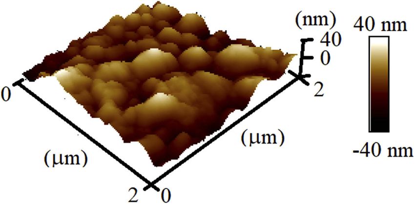
Research Article                                 Vol. 28, No. 10 / 11 May 2020 / Optics Express 15708

the result of rough rear surface to enable more accurate ellipsometric measurements. It should be
noted that although FTO-coated substrates were used in this work, this is not important as even if
the CsPbBr3 thin film has been deposited on a bare glass substrate, the rear side would still need
to be mechanically roughened rear before VASE experiments and analysis.
   The pressing of CsPbBr3 thin films is conducted using an in-house hot-embossing machine
[21–23]. The sample for hot embossing is placed between the upper and lower stainless steel
plates and the substrate can be heated up. In this work, the sample size is 2 cm × 2 cm. A
polished silicon wafer is used as a mold in order to achieve a smooth CsPbBr3 surface with
low surface roughness. To compare difference between the hot-embossed and non-embossed
regions of the sample, the mold size is smaller than the size of the sample. A force of 30000
N is applied for the present experiment. It is necessary to point out that too large force can
break the sample while too small force is not effective in significantly reducing the surface
roughness. The present hot embossing of CsPbBr3 film referred to a previous report on a
perovskite Cs0.1 (MA0.17 FA0.83 )0.9 Pb(I0.83 Br0.17 )3 thin film [23]. We found that the substrate
temperature of 60 °C can significantly decrease the surface roughness from 35 nm to 9 nm for
CsPbBr3 thin film, which is good enough to achieve the purpose of this work for experimental
determination on the complex optical constants of the CsPbBr3 thin films. The mold pressing
time is 20 min. When the hot embossing is finished, the sample is left to cool down to room
temperature and then is demolded.

2.2.    Characterization
X-ray diffraction (XRD) spectra are collected with a diffractometer (Bruker D-8 Advance)
using Cu Kα X-ray radiation to investigate the crystalline structure. The wavelength dependent
transmission and absorption of the sample are conducted by using a spectrophotometer equipped
with an integrating sphere (Perkin Elmer Lambda 950). The photoluminescence (PL) spectrum
is measured (Hitachi F-4600) to compare with the bandgap of the CsPbBr3 obtained from the
Tauc plot method. Scanning electron microscopy (SEM, Zeiss Supra 60VP) images are obtained
in order to assess the surface morphology and film thickness. An atomic force microscope
(AFM, Bruker Dimension Icon) is used to investigate surface roughness of the samples. A VASE
(M-2000 F, J. A. Woollam Co. Inc) is the main tool used to measure ellipsometry output data (Ψ
and ∆), with measurements conducted at three angles: 45°, 55°, and 65°. The estimated diameter
of beam spot used in the present ellipsometry measurements at the three angles is 1.5-2 mm.
Besides, the Sentech spectroscopic ellipsometry instrument (Model: SENresearch 4.0, Germany)
is also used to assess the measurement uncertainty of the optical constants, where the beam spot
size is 2-4 mm. The adopted models for the fitting to the ellipsometric data are the same between
the two instrument measurements.

2.3.    WVASE model and photocurrent density simulations
In order to determine the n and k of the CsPbBr3 thin film, a commercial software package
(WVASE32 v.3.888, J. A. Woollam) is employed to construct a proper model to fit the ellipsometric
data Ψ and ∆. As we know, an ideal thin film that is homogenous and exhibits perfectly flat
surfaces rarely occurs in the real world. The most commonly encountered cases are non-ideal
thin film such as surface roughness at the top, thickness variation, and a variation of the optical
constants from top to bottom throughout the film [24].
   The ellipsometric parametersΨ and ∆ can be related to the ratio of Fresnel reflection coefficients
Rp and Rs for p- and s-polarized light as described in Eq. (1) :

                                             Rp
                                        ρ=      = tan(ψ)ei∆                                              (1)
                                             Rs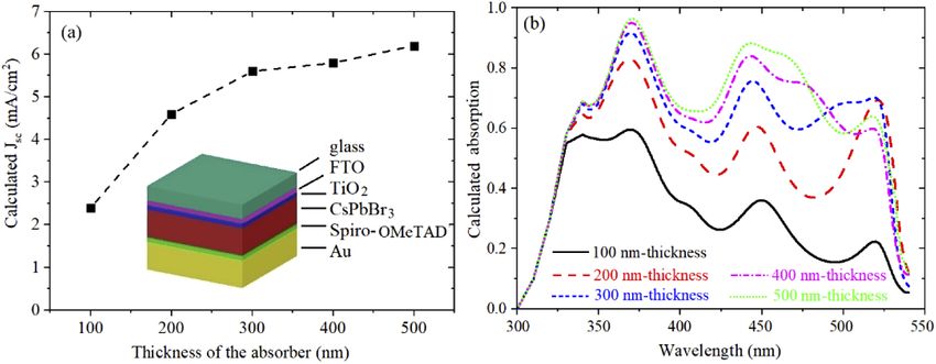
Research Article                                         Vol. 28, No. 10 / 11 May 2020 / Optics Express 15709

The VASE technique measures the ratio of the two values and as a result, the measured results
are highly accurate and reproducible [24]. For the present sample (CsPbBr3 perovskite thin film
on a glass substrate), the Cauchy dispersion function is used to describe the property of the
glass substrate. In the model for the CsPbBr3 layer, the perovskite thin film is divided into (or
equivalent to) two parts. The one is bulk planar perovskite layer (the bulk thickness is defined as
dbulk ). The other is a surface roughness layer consisting of the mixture of air void and perovskite
material (vertical surface roughness of this layer is defined as drough ). To illustrate this model, a
drawing of the CsPbBr3 layer is shown in Fig. 4(a). For the surface roughness layer, a Bruggeman
effective medium approximation (EMA) is usually suitable, whereby the medium consists of
the mixture of x% air void and (100 – x)% perovskite material, where x can take a value in the
range from 0 to 100. For bulk perovskite layer (dbulk ), the oscillators such as Tauc-Lorentz (T-L)
and Gaussian (Gau) were successfully used to describe the dielectric function of the perovskites
[14–18]. The T-L oscillator function and Gau oscillator function are expressed in Eq. (2) - Eq.
(4), respectively [24]:
                                        εn_T−L = εn1 + iεn2                                       (2)
where, when E ≤ Egn , εn2 = 0; when E>Egn ,

                                     An Eon Cn (E − Egn )2 1
                                   "                         #
                             εn2 =               2
                                                          ×                                                    (3)
                                     (E2 − Eo2n ) + Cn2 E2 E

In Eqs. (2) and (3), the subscript T-L indicates that the model is based on the Tauc joint density
of states and the Lorentz oscillator. These four fitting parameters are An , Eon , Cn , and Egn , where
these parameters are in units of energy of eV.

                                         εn_Gau = εn1 + iεn2                                                   (4)

where,
                                                   ∫∞
                                             2             ξεn2 (ξ)
                                      εn1   = P                     dξ
                                             π             ξ 2 − E2
                                                   0

                                              −( E−E n 2             E+En 2
                                   εn2 = An       σ )      − An −(    σ )

                                                Brn
                                            σ= p
                                              2 ln(2)
In Eq. (4), the subscript Gau indicates that the model is based on the Gaussian oscillator. The
three fitting parameters that are used for the WVASE fitting are An , where the unit is dimensionless,
En , where the unit is eV, and Brn , where the unit is eV.
   Several studies have pointed out that variation of the optical constants of a thin film along the
direction normal to the film (i.e. vertically through the film) is most commonly caused by the
drifting of process parameters during the deposition of the film or induced by post-deposition
processing of the film such as annealing [24]. In the preparation of the present CsPbBr3 thin films,
a two-step deposition was used, where a heating at 250 °C for 5 min was involved. Furthermore,
the sample was heated at 60 °C for 20 min during the hot embossing, which can be regarded as a
low temperature annealing. These facts suggest that the model of one-dimensional graded index
along the direction normal to the film could be considered. Graded layers work by creating a
series of homogenous layers with optical constants that change slightly in each layer.
   Regarding the calculation of light absorption and Jsc of the CsPbBr3 solar cells, the light
absorption power, Pabs , is calculated from the divergence of the Poynting vector using the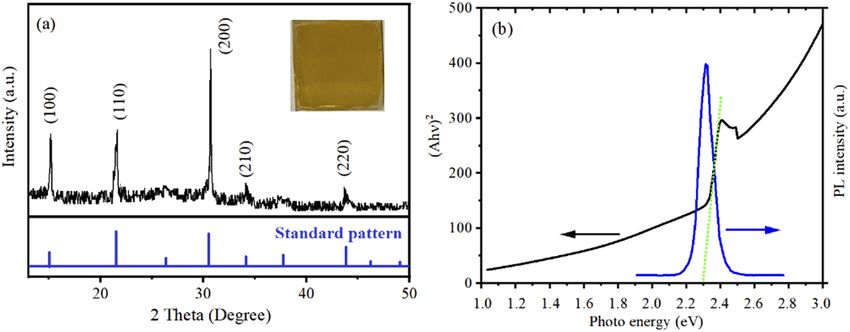
Research Article                                      Vol. 28, No. 10 / 11 May 2020 / Optics Express 15710

following equation:
                                        Pabs = 0.5ωεim |E(ω)| 2                                             (5)
where ω is the angular frequency, εim is the imaginary part of the permittivity, and E is the
electric field. During the present simulations, the normalized light absorptivity in the perovskite
absorber can be determined by:
                                      A(λ) = Pabs (λ)/Pin (λ)                                   (6)
where Pin (λ) is the power of incident light within the solar cell at a wavelength λ. Here, we
assume that all generated electron-hole pairs are extracted and collected – in other words, a unity
quantum efficiency – such that the Jsc can be calculated by integrating light absorption A(λ) over
all wavelengths as follows:
                                       ∫
                               Jsc = e λ/hc × A(λ)IAM1.5 (λ)dλ                                  (7)

where, e is the charge of an electron in the unit of C. h is Plank’s constant in the unit of J·s. c is
the speed of light in free space with the unit of m/s, and A(λ) is the light absorption as function
of wavelength. IAM 1.5 is air mass 1.5 global solar spectrum with unit of W/m2 /nm.

3.   Results and discussion
The measured XRD pattern of the as-prepared CsPbBr3 thin film on the bare glass substrate is
shown in Fig. 1(a), where the inset is a photo of the sample and a standard XRD pattern of a
cubic CsPbBr3 is cited from Ref. [25]. The XRD result indicates that the crystal structure of
CsPbBr3 is in a cubic (Pm3 m) phase and falls within a standard XRD pattern reported for a
cubic CsPbBr3 phase [25]. However, it is noted that compared with the standard pattern, some of
small peaks are not detected as they are too weak, as is also sometimes reported in the literature
[6,7,25,26]. After hot embossing of the CsPbBr3 thin film at 60 °C, the crystalline structure
remains unchanged. By using a Tauc plot for the measured wavelength-dependent transmission
of the hot-embossed CsPbBr3 thin film (∼400 nm thickness) in the wavelength range of 300 to
1100 nm, the optical bandgap is estimated from the plotting of (Ahv)2 versus photon energy (hv)
as shown in Fig. 1(b). It is found that the present CsPbBr3 perovskite film exhibits a direct
bandgap of 2.3 eV, consistent with previous reports [7,9,27]. The PL spectrum of CsPbBr3 thin
film is measured and shown in Fig. 1(b). The obtained bandgap is 2.3 eV, which is consistent

       Fig. 1. (a) XRD pattern of the present CsPbBr3 thin film on glass substrate, where the inset
       is a sample photo and a standard XRD pattern of a cubic CsPbBr3 is included. (b) Tauc plot
       of (Ahv)2 versus photon energy (hv) in order to estimate the optical bandgap (green dotted
       line), which is confirmed via the PL spectrum.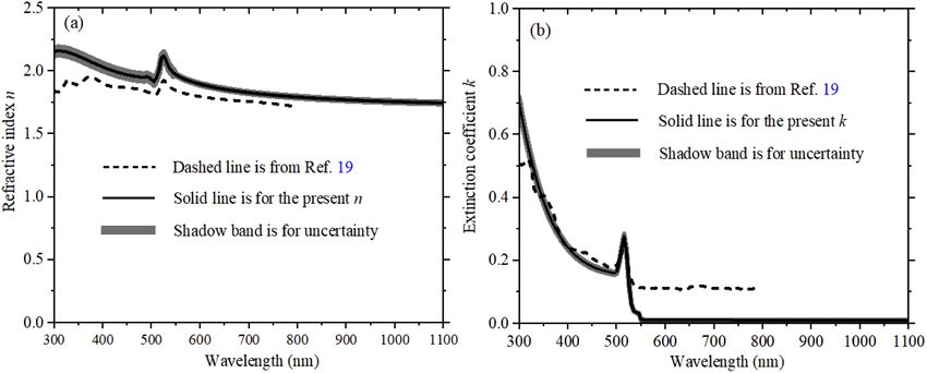
Research Article                                  Vol. 28, No. 10 / 11 May 2020 / Optics Express 15711

with the bandgap determined from the Tauc-plot method. Specifically, via the Tauc-plot method,
the obtained bandgap is 540 nm, while from PL measurements the peak is at 537 nm.
   Top-view SEM morphologies of the CsPbBr3 thin film at two different magnifications are shown
in Figs. 2(a) and 2(b). The morphology difference between hot embossed and non-embossed
regions are clearly visible, with the top half of the image region has no hot embossing and
bottom half region has hot embossing. It is clearly seen in both Figs. 2(a) and 2(b) that the
smooth degree of the CsPbBr3 surface has been obviously improved by the hot embossing. This
indicates that hot embossing can significantly reduce the degree of surface roughness. Figure 2(c)
shows a cross-section image of the hot-embossed CsPbBr3 thin film and the estimated thickness
is 395 nm. To assess the surface roughness of the interested embossed region, a measured
three-dimensional (3D) AFM image is shown in Fig. 3. The RMS surface roughness value is
9 nm for the hot-embossed region, while for the non-embossed region the average RMS roughness
is ∼35 nm. It should be pointed out that the RMS surface roughness of 9 nm as shown in Fig. 3
is for a single measurement. We have made roughness measurements at different regions and the
variation is ± 2 nm.

       Fig. 2. (a) Top-view SEM image of the CsPbBr3 thin film, where top half region has no
       hot embossing and bottom half region has hot embossing. (b) A higher magnification SEM
       image of the CsPbBr3 thin film. (c) Cross-sectional SEM image of the embossed CsPbBr3
       thin film.

   Figure 4(a) shows a schematic of a perovskite CsPbBr3 thin film on a bare glass substrate.
Figure 4(b) is the established model to fit the measured Ψ and ∆, where an EMA model with
50% of air void is used to describe rough CsPbBr3 surface; one-dimensional graded-index model
through the film from bottom to top combined with one T-L oscillator and two Gau oscillators
are used to describe the bulk flat CsPbBr3 layer; The Cauchy dispersion model is used to describe
the glass substrate, where it is a soda-lime glass. The measured and fitted Ψ and ∆ at the angles
of 45°, 55°, and 65° are presented in Figs. 4(c) and 4(d) in the wavelength range of 300 to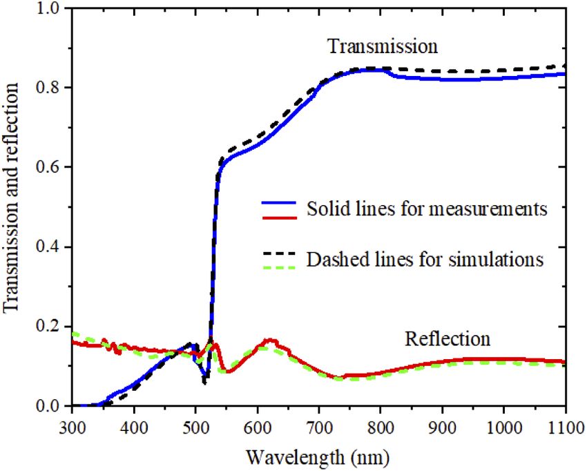
Research Article                                     Vol. 28, No. 10 / 11 May 2020 / Optics Express 15712

            Fig. 3. AFM images of the hot-embossed CsPbBr3 thin film with the size of 2 µm by 2 µm
            in 3D view.

1100 nm, respectively. It can be seen that very good fitting results are achieved for both Ψ and ∆.
Via the optimization, it is found the best fitting results are as follows: a graded index variation
of 11% from the bottom to top through the perovskite thin film; one T-L oscillator and two
Gau oscillators; thicknesses of the bulk perovskite layer and the surface roughness extracted
from the fitting results are 402 nm and 10 nm, respectively, which are both in close agreement
with the SEM and AFM results. Finally, the extracted parameters from the best fitting and the
estimated values from the measurements are summarized in Table 1. It is further found that if
either the graded index model was not included or all oscillators fully adopts T-L oscillators, the
fitting results are worsened causing serious deviation of the optical constants. In contrast, if all
oscillators adopts Gau oscillators, the optical constants are affected slightly.

 Table 1. The extracted parameters from the best fitting using M-2000 F (J. A. Woollam Co. Inc) and
                                  the experimental estimation.
Oscillators              An                    En or Eon (eV)        Cn                Egn (eV)             Brn (eV)
1: T-L                   295.6 (eV)            2.42                  0.035             2.60
2: Gau                   0.95                  2.40                                                         0.07
3: Gau                   5.75                  5.43                                                         2.71
drough :                10 nm (VASE result)                         9 ± 2 nm (AFM result)
dbulk :                 403 nm (VASE result)                        395 ± 10 nm (SEM result)
Refractive index variation: 11% (fitting result)

   From the above best fitting results, we can obtain the dispersive n and k values. Their results
are shown in Fig. 5 using solid lines, where the reported optical constants of a CsPbBr3 thin film
in the wavelength range of 300-800 nm are cited from Ref. [19] for comparison and discussion.
On the one hand, compared with Ref. [19], the overall trends in n and k values are similar in the
wavelength range of 300 to 800 nm. On the other hand, our n values are obviously higher than
that of the report in this wavelength range. In addition, we extend the complex optical constants to
longer wavelength of 1100 nm, which offers a unique opportunity to do design and simulations on
high-efficiency CsPbBr3 /c-Si tandem solar cells. It was noted that a high RMS surface roughness
of 37 nm could result in an underestimation of the refractive index (n = 1.93 at about 525 nm)
Research Article Vol. 28, No. 10 / 11 May 2020 / Optics Express 15713
Fig. 4. (a) Schematic diagram of the present sample structure consisting of perovskite
CsPbBr3 thin film on glass substrate with the roughened rear surface. (b) Established model
for the present fitting. (c) The measured and fitted Ψ at the three angles of 45°, 55°, and 65°
in the wavelength range of 300 to 1100 nm. (d) The measured and fitted ∆ at the angles of
45°, 55°, and 65° in the wavelength range of 300 to 1100 nm.
values [19]. It is found that at the wavelength of 525 nm, the n value obtained from this work is
2.12, which indicates that our n value is 10% larger than the report at this wavelength. Regarding
a comparison of k values, one main difference is that in the present work, the k values approach
zero for wavelengths greater than 550 nm whereas the k values in the report remain at around
0.11. The k values being zero at longer wavelengths means that the CsPbBr3 thin film becomes
non-absorptive. Thus, it is suitable to develop high-efficiency CsPbBr3 /c-Si tandem solar cells,
which are based on the working principle that top semi-transparent perovskite cell and bottom
c-Si solar cell can absorb the shorter (300-550 nm) and longer (550-1100 nm) wavelengths of
sunlight, respectively. In this way, such tandem solar cell (for example, a four-terminal device)
has the potential to produce a power conversion efficiency exceeding the Shockley-Queisser limit.
To assess the uncertainty of the optical constants of the CsPbBr3 thin films, the ellipsometric
measurements are conducted on both different regions of a single sample and on different samples,
where the assessments are extended to include a different ellipsometry instrument (Sentech) as
well. For the measurements on the two instrument, the beam spot sizes are different as described
in the characterization section and the adopted models are the same for the ellipsometric fitting.
The results of the uncertainty are shown in Fig. 5 using shadow bands, where the solid lines are
for the best result based on J. A. Woollam instrument and the shadow bands are the uncertainty
for all results based on the two instruments. It is found that the variation of the obtained optical
constants of CsPbBr3 is less than 3% compared with the result of Fig. 5 in solid lines. To
further check the validity of the obtained optical constants, the comparison of transmission and
reflection between the measurements and simulations in the wavelength range of 300 to 1100 nm
is plotted in Fig. 6. It can be seen that good agreement between the measurement and calculatedResearch Article Vol. 28, No. 10 / 11 May 2020 / Optics Express 15714
spectrophotometric data is achieved, thus giving further confidence to the n and k values extracted
from VASE measurements.
Fig. 5. (a)The determined refractive index (n) of the CsPbBr3 thin film in the wavelength
range of 300 to 1100 nm as shown in solid line, where the measurement uncertainty is shown
using shadow band. For comparison, a report regarding complex optical constants of a
CsPbBr3 thin film in the wavelength rang of 300 to 800 nm is cited as shown in dashed
lines. (b) The obtained extinction coefficient (k) result, measurement uncertainty, and the
comparison with Ref. [19].
Fig. 6. The measured and simulated transmission and reflection in the wavelength range of
300 to 1100 nm, where solid lines are for measurements and dashed lines are for simulations.
Once the complex optical constants of CsPbBr3 thin films are obtained, the photovoltaic (PV)
device design can be conducted via the FDTD simulations. The optical constants of other required
materials are well established and can be taken from literature. In the present work, as an example
demonstration, we focus on single-junction CsPbBr3 solar cells to conduct investigations on the
light absorption and Jsc . Because the CsPbBr3 thin films have the optical bandgap of 2.3 eV,Research Article Vol. 28, No. 10 / 11 May 2020 / Optics Express 15715
the spectral response range of the PV application of the CsPbBr3 solar cells is from 300 nm to
around 540 nm. It is confirmed by a PV device report, where when the wavelengths are greater
than 540 nm, the external quantum efficiency (EQE) of the CsPbBr3 solar cells becomes zero
[9]. It means that to investigate light absorption and photocurrent density of the single-junction
CsPbBr3 solar cells (2.3 eV bandgap) for PV application, it is fair and sufficient to limit the
wavelength range to 300-540 nm.
The constructed CsPbBr3 solar cell schematic is shown in Fig. 7(a), where the absorber
thicknesses are varied from 100 to 500 nm with an interval of 100 nm to investigate the effect
of the absorber thickness on the light absorption and Jsc . The thicknesses of FTO, titanium
dioxide (TiO2 ), 2,2’,7,7’-Tetrakis[N,N-di(4-methoxyphenyl)amino]-9,9’-spirobifluorene (Spiro-
OMeTAD), and gold (Au) layers are set as 400 nm, 50 nm, 50 nm, and 300 nm, respectively.
Correspondingly, the complex optical constants of FTO, TiO2 , and Spiro-OMeTAD for simulations
are cited from the reported measurements [28] and the optical constants of Au and soda lime
glass are taken from the literature [29]. In the present simulations, the soda lime glass substrate
is included with the thickness of 2 mm, where complex optical constants are taken from the
literature [30]. The calculated Jsc as a function of the absorber thickness is shown in Fig. 7(a).
It is seen that the Jsc increases with the absorber thickness. When the absorber thickness is
100 nm, the Jsc value is as low as 2.4 mA/cm2 . When the absorber thickness increases from
100 nm to 300 nm, the Jsc increases significantly from 2.4 to 5.6 mA/cm2 with an enhancement
of 2.3 times, which can be understood from the calculated light absorption as shown in Fig.
7(b). It can be seen in Fig. 7(b) that compared to the light absorption of 100 nm-thick absorber,
the absorption in the 200 nm- and 300 nm-thick absorbers presents a whole broadband light
absorption enhancement in the wavelength range of around 350-540 nm. In contrast, as shown in
Fig. 7(a), the Jsc presents a small increase when the absorber thicknesses are further increased
from 300 nm to 500 nm. Specifically, the photocurrent density values are 5.8 and 6.2 mA/cm2 for
the absorber thicknesses of 400 nm and 500 nm, respectively. This indicates that the absorber
thickness should be 300 nm at least to acquire a good light absorption. It is noted in Fig. 7(b)
that the calculated light absorption at the wavelength of 540 nm is not zero, which is because the
obtained extinction coefficient k value does not exactly reach zero at this wavelength. However,
its effect on the calculated Jsc values is so small that can be neglected.
Fig. 7. (a) Calculated Jsc values of the CsPbBr3 cells with the absorber thickness varying
from 100 to 500 nm with an interval of 100 nm. (b) Calculated absorption in the CsPbBr3
absorbers versus wavelength.Research Article Vol. 28, No. 10 / 11 May 2020 / Optics Express 15716
4. Conclusions
The complex optical constants of the CsPbBr3 thin films were determined via the VASE
measurements at three variable angles for the hot-embossed CsPbBr3 thin films and the constructed
model, where one-dimensional simple graded-index model and the EMA model with 50% air
void were used to describe bulk perovskite and rough surface. The transmission and reflectance
between the measurement and simulation show a good agreement. The obtained optical constants
enable to implement the design and simulations of the CsPbBr3 based PV device. As a
representative example demonstration, the photocurrent densities were investigated for single-
junction CsPbBr3 solar cells with varying absorber thickness, which can be understood from
the calculated wavelength dependent light absorption. These results enable to help to improve
the efficiency of single-junction CsPbBr3 solar cells and develop high-efficiency CsPbBr3 /c-Si
tandem solar cells via the design and simulations.
Funding
A Recruitment Initiative Fellowship from Helmholtz Association; Science and Technology of
Nanosystems research programme; Helmholtz Materials Energy Foundry; Deutsche Forschungs-
gemeinschaft (YA516/1-1); National Natural Science Foundation of China (21573108, 21872069,
51761135104); National Key Research and Development Program of China (2016YFB0700600,
2017YFA0208200); Natural Science Foundation of Jiangsu Province (BK20180008); Fundamen-
tal Research Funds for the Central Universities (0205-14380188).
Acknowledgments
This work was partially carried out with the support of the Karlsruhe Nano Micro Facility
(KNMF) at Karlsruhe Institute of Technology (KIT). The technical support from the KNMF
includes the hot embossing instrument, AFM and SEM. They also acknowledge Dr. Ulrich W.
Paetzold for hot embossing suggestions.
Disclosures
The authors declare that there are no conflicts of interest related to this article.
References
1. A. Kojima, K. Teshima, Y. Shirai, and T. Miyasaka, “Organometal halide perovskites as visible-light sensitizers for
photovoltaic cells,” J. Am. Chem. Soc. 131(17), 6050–6051 (2009).
2. NREL, Best research-cell efficiency chart, https://www.nrel.gov/pv/cell-efficiency.html, access on April 17, 2019.
3. Y. G. Rong, Y. Hu, A. Y. Mei, H. R. Tan, M. I. Saidaminov, S. Seok, M. D. McGehee, E. H. Sargent, and H. W. Han,
“Challenges for commercializing perovskite solar cells,” Science 361(6408), eaat8235 (2018).
4. M. Kulbak, D. Cahen, and G. Hodes, “How important is the organic part of lead halide perovskite photovoltaic cells?
efficient CsPbBr3 cells,” J. Phys. Chem. Lett. 6(13), 2452–2456 (2015).
5. R. J. Sutton, G. E. Eperon, L. Miranda, E. S. Parrott, B. A. Kamino, J. B. Patel, M. T. Hörantner, M. B. Johnston, A.
A. Haghighirad, D. T. Moore, and H. J. Snaith, “Bandgap-tunable cesium lead halide perovskites with high thermal
stability for efficient solar cells,” Adv. Energy Mater. 6(8), 1502458 (2016).
6. R. E. Beal, D. J. Slotcavage, T. Leijtens, A. R. Bowring, R. A. Belisle, W. H. Nguyen, G. F. Burkhard, E. T. Hoke,
and M. D. McGehee, “Cesium lead halide perovskites with improved stability for tandem solar cells,” J. Phys. Chem.
Lett. 7(5), 746–751 (2016).
7. J. Liang, C. Wang, Y. Wang, Z. Xu, Z. Lu, Y. Ma, H. Zhu, Y. Hu, C. Xiao, X. Yi, G. Zhu, H. Lv, L. Ma, T. Chen, Z.
Tie, Z. Jin, and J. Liu, “All-inorganic perovskite solar cells,” J. Am. Chem. Soc. 138(49), 15829–15832 (2016).
8. M. Kulbak, S. Gupta, N. Kedem, I. Levine, T. Bendikov, G. Hodes, and D. Cahen, “Cesium enhances long-term
stability of lead bromide perovskite-based dolar cells,” J. Phys. Chem. Lett. 7(1), 167–172 (2016).
9. K. C. Tang, P. You, and F. Yan, “Highly stable all-inorganic perovskite solar cells processed at low temperature,” Sol.
RRL 2(8), 1800075 (2018).
10. J. Lei, F. Gao, H. X. Wang, J. Li, J. X. Jiang, X. Wu, R. R. Gao, Z. Yang, and S. Z. (Frank) Liu, “Efficient planar
CsPbBr3 perovskite solar cells by dual-source vacuum evaporation,” Sol. Energy Mater. Sol. Cells 187, 1–8 (2018).Research Article Vol. 28, No. 10 / 11 May 2020 / Optics Express 15717
11. H. W. Yuan, Y. Y. Zhao, J. L. Duan, Y. D. Wang, X. Y. Yang, and Q. W. Tang, “All-inorganic CsPbBr3 perovskite
solar cell with 10.26% efficiency by spectra engineering,” J. Mater. Chem. A 6(47), 24324–24329 (2018).
12. X. Y. Liu, X. H. Tan, Z. Y. Liu, H. B. Ye, B. Sun, T. L. Shi, Z. R. Tang, and G. L. Liao, “Boosting the efficiency of
carbon-based planar CsPbBr3 perovskite solar cells by a modified multistep spin-coating technique and interface
engineering,” Nano Energy 56, 184–195 (2019).
13. Y. Y. Zhao, T. S. Liu, F. M. Ren, J. L. Duan, Y. D. Wang, X. Y. Yang, Q. H. Li, and Q. W. Tang, “Organic
hole-transporting materials for 9.32%-efficiency and stable CsPbBr3 perovskite solar cells,” Mater. Chem. Front.
2(12), 2239–2244 (2018).
14. P. Löper, M. Stuckelberger, B. Niesen, J. Werner, M. Filipič, S.-J. Moon, J.-H. Yum, M. Topič, S. De Wolf, and
C. Ballif, “Complex refractive index spectra of CH3 NH3 PbI3 perovskite thin films determined by spectroscopic
ellipsometry and spectrophotometry,” J. Phys. Chem. Lett. 6(1), 66–71 (2015).
15. Y. J. Jiang, M. A. Green, R. Sheng, and A. Ho-Baillie, “Room temperature optical properties of organic–inorganic
lead halide perovskites,” Sol. Energy Mater. Sol. Cells 137, 253–257 (2015).
16. M. S. Alias, I. Dursun, M. I. Saidaminov, E. M. Diallo, P. Mishra, T. K. N. G. O, M. Bakr, and B. S. Ooi, “Optical
constants of CH3 NH3 PbBr3 perovskite thin films measured by spectroscopic ellipsometry,” Opt. Express 24(15),
16586–16594 (2016).
17. S. Brittman and E. C. Garnett, “Measuring n and k at the microscale in single crystals of CH3 NH3 PbBr3 perovskite,”
J. Phys. Chem. C 120(1), 616–620 (2016).
18. C. W. Chen, S. Y. Hsiao, C. Y. Chen, H. W. Kang, Z. Y. Huang, and H. W. Lin, “Optical properties of organometal
halide perovskite thin films and general device structure design rules for perovskite single and tandem solar cells,” J.
Mater. Chem. A 3(17), 9152–9159 (2015).
19. M. L. Zhao, Y. J. Shi, J. Dai, and J. Lian, “Ellipsometric study of the complex optical constants of a CsPbBr3
perovskite thin film,” J. Mater. Chem. C 6(39), 10450–10455 (2018).
20. W. S. Yan, Y. Guo, D. Beri, S. Dottermusch, H. N. Chen, and B. S. Richards, “Experimental determination of complex
optical constants of air-stable inorganic CsPbI3 perovskite thin films,” Phys. Status Solidi RRL, 2000070 (2020).
21. W. S. Yan, Y. Huang, L. Wang, F. Vüllers, M. N. Kavalenka, H. Hölscher, S. Dottermusch, B. Richards, and E.
Klampaftis, “Photocurrent enhancement for ultrathin crystalline silicon solar cells via a bioinspired polymeric nanofur
film with high forward scattering,” Sol. Energy Mater. Sol. Cells 186, 105–110 (2018).
22. F. Vüllers, G. Gomard, J. B. Preinfalk, E. Klampaftis, M. Worgull, B. Richards, H. Hölscher, and M. N. Kavalenka,
“Bioinspired superhydrophobic highly transmissive films for optical applications,” Small 12(44), 6144–6152 (2016).
23. R. Schmager, J. Roger, J. A. Schwenzer, F. Schackmar, T. Abzieher, M. M. Byranvand, B. A. Nejand, M. Worgull, B.
S. Richards, and U. W. Paetzold, “Laminated perovskite photovoltaics: enabling novel layer combinations and device
architectures,” Adv. Funct. Mater. 30(9), 1907481 (2020).
24. J. A. Woollam ellipsometry solutions, Guide to using WVASE spectroscopic ellipsometry data acquisition and
analysis software (https://www.jawoollam.com).
25. Z. F. Shi, L. Z. Lei, Y. Li, F. Zhang, Z. Z. Ma, X. J. Li, D. Wu, T. T. Xu, Y. T. Tian, B. L. Zhang, Z. Q. Yao, and G. T.
Du, “Hole-injection layer-free perovskite light-emitting diodes,” ACS Appl. Mater. Interfaces 10(38), 32289–32297
(2018).
26. Z. H. Wei, A. Perumal, R. Su, S. Sushant, J. Xing, Q. Zhang, S. T. Tan, H. V. Demir, and Q. H. Xiong,
“Solution-processed highly bright and durable cesium lead halide perovskite light-emitting diodes,” Nanoscale 8(42),
18021–18026 (2016).
27. G. Q. Tong, L. K. Ono, and Y. B. Qi, “Recent progress of all-bromide inorganic perovskite solar cells,” Energy
Technol. (Weinheim, Ger.) 8(4), 1900961 (2020).
28. J. M. Ball, S. D. Stranks, M. T. Hörantner, S. Hüttner, W. Zhang, E. J. W. Crossland, I. Ramirez, M. Riede, M. B.
Johnston, R. H. Friend, and H. J. Snaith, “Optical properties and limiting photocurrent of thin-film perovskite solar
cells,” Energy Environ. Sci. 8(2), 602–609 (2015).
29. E. D. Palik, Handbook of Optical Constants of Solids (Elsevier, New York, 1998).
30. M. Rubin, “Optical properties of soda lime silica glasses,” Sol. Energy Mater. 12(4), 275–288 (1985).You can also read