Development and characterization of Nb3Sn/Al2O3 superconducting multilayers for particle accelerators - Nature
←
→
Page content transcription
If your browser does not render page correctly, please read the page content below
www.nature.com/scientificreports
OPEN Development and characterization
of Nb3Sn/Al2O3 superconducting
multilayers for particle accelerators
Chris Sundahl1, Junki Makita2, Paul B. Welander3, Yi‑Feng Su4, Fumitake Kametani4,5,
Lin Xie6, Huimin Zhang7, Lian Li7, Alex Gurevich2* & Chang‑Beom Eom1*
Superconducting radio-frequency (SRF) resonator cavities provide extremely high quality factors > 1010
at 1–2 GHz and 2 K in large linear accelerators of high-energy particles. The maximum accelerating
field of SRF cavities is limited by penetration of vortices into the superconductor. Present state-of-the-
art Nb cavities can withstand up to 50 MV/m accelerating gradients and magnetic fields of 200–240
mT which destroy the low-dissipative Meissner state. Achieving higher accelerating gradients requires
superconductors with higher thermodynamic critical fields, of which Nb3Sn has emerged as a leading
material for the next generation accelerators. To overcome the problem of low vortex penetration
field in Nb3Sn, it has been proposed to coat Nb cavities with thin film Nb3Sn multilayers with dielectric
interlayers. Here, we report the growth and multi-technique characterization of stoichiometric
Nb3Sn/Al2O3 multilayers with good superconducting and RF properties. We developed an adsorption-
controlled growth process by co-sputtering Nb and Sn at high temperatures with a high overpressure
of Sn. The cross-sectional scanning electron transmission microscope images show no interdiffusion
between Al2O3 and Nb3Sn. Low-field RF measurements suggest that our multilayers have quality
factor comparable with cavity-grade Nb at 4.2 K. These results provide a materials platform for
the development and optimization of high-performance SIS multilayers which could overcome the
intrinsic limits of the Nb cavity technology.
For decades, Nb has been the material of choice for the radio-frequency superconducting (SRF) resonators for
high-energy particle accelerators. Technological advances have resulted in the development of Nb cavities which
can exhibit extremely high quality factors Q > 1010 @ 1–2 GHz and 2 K while sustaining accelerating gradients
up to 50 MV/m1–3. Such exemplary performance and low RF losses can only be achieved if the cavities operate
in a Meissner state which can persist up to the maximum magnetic field at the inner cavity surface reaches the
superheating field Bs = 240 mT1–3. At B = Bs the low-dissipative Meissner state becomes absolutely unstable with
respect to dissipative penetration of vortices, causing an explosive increase of RF power and thermal quench of
the cavity. The state-of-the-art Nb cavities can already operate at the peak magnetic field close to B s, thus, increas-
ing accelerating gradients beyond the intrinsic limits of Nb requires materials with higher Bs. There are many such
materials but all of them are type-II superconductors with lower critical field B c1 smaller than Bc1 ≈ 170−180
mT of Nb which makes high-Bs superconductors prone to detrimental penetration of vortices at low fi elds4,5.
To overcome this problem, it was proposed to nanostructure the inner surface of Nb cavities by coating it with
multilayers of thin superconductors (S) separated by dielectric insulating (I) layers (Fig. 1)6. Here the S-layer
material has a superheating field B s higher than B s0 of Nb, whereas the thickness d of S layers is smaller than the
London penetration depth , and the thickness of I layers can be a few nm to suppress the interlayer Josephson
coupling. Such SIS structures greatly increase barriers for penetration of vortices in the bulk of the cavity which
could potentially withstand the RF fields limited by the superheating field of S-layer. For instance, using N b3Sn
with Bs = 480 mT could nearly double the maximum accelerating gradient as compared to the best Nb cavities.
The multilayer approach is based on the lack of thermodynamically stable parallel vortices in thin decoupled S
1
Department of Materials Science and Engineering, University of Wisconsin-Madison, Madison, WI 53706,
USA. 2Physics Department and Center for Accelerator Science, Old Dominion University, Norfolk, VA 23529,
USA. 3SLAC National Accelerator Laboratory, Menlo Park, CA 94025, USA. 4Applied Superconductivity Center,
National High Magnetic Field Laboratory, Florida State University, Tallahassee, FL 32310, USA. 5Department of
Mechanical Engineering, FAMU-FSU College of Engineering, Tallahassee, FL 32310, USA. 6Department of Physics,
Southern University of Science and Technology, Shenzhen 518055, China. 7Department of Physics and Astronomy,
West Virginia University, Morgantown, WV 26506, USA. *email: agurevic@odu.edu; eom@engr.wisc.edu
Scientific Reports | (2021) 11:7770 | https://doi.org/10.1038/s41598-021-87119-9 1
Vol.:(0123456789)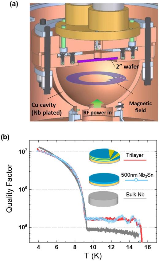
www.nature.com/scientificreports/
Figure 1. Schematic of Nb3Sn/Al2O3 multilayer heterostructures on Al2O3 wafer. Back side of Al2O3 wafer is
coated with a thick Nb film.
screens at B < Bc1 where Bc1 is strongly enhanced in films with d < 6–10. Because the inner surface of the Nb
cavity is partially screened by multilayers, both Q(H) and the breakdown field can be increased due to lower
surface resistance R s and higher H c of the layer material6.
The multilayer coating, which opens up a principal opportunity to break the Nb monopoly in SRF cavities,
has been tested by several groups using MgB2, Nb3Sn, NbN, NbTiN, and dirty Nb as coating materials. These
experiments have shown an increase of the dc field onset of penetration of vortices on Nb surfaces coated with
different SIS s tructures4,11–19, although such key SRF characteristics as the surface resistance and quality factors
of SIS multilayers under high-amplitude RF fields have been investigated to a much lesser extent. The first results
on low-field Q measurements on NbN/MgO m ultilayers13,19 have shown that SIS multilayers can have lower R
s
than bulk Nb. However, the SRF performance of Nb3Sn, the current material of choice for the next generation
coating material20, has not yet been investigated in SIS structures. The development of SIS structures requires
overcoming many materials science and technological challenges to achieve good superconducting properties
and SRF performance while providing optimal stoichiometry and morphology of the layers and the interfaces
and transparency of grain boundaries to extremely high RF current densities. In this work we report results on
growth and characterizations of N b3Sn/Al2O3 multilayers which exhibit good superconducting properties and
low-field SRF performance on par with the cavity-grade Nb.
Results and discussion
Multilayer growth. We developed a technique of high-temperature confocal sputtering of Nb and Sn from
elemental targets to grow stoichiometric N b3Sn multilayers with A l2O3 interlayers. Details are given in the Sup-
plemental Information. Thin films and multilayers of different thicknesses were grown on different sapphire
single crystal substrates for the subsequent characterizations. For instance, 60 nm thick Nb3Sn films were grown
on 10 × 10 mm sapphire substrates for transport, scanning tunneling spectroscopy and electron microscopy
characterizations. For RF tests, we grew Nb3Sn/Al2O3 multilayers on 2″ diameter sapphire wafers (R-plane,
300 μm thick). These multilayers had up to three 60 nm Nb3Sn layers separated by 6 nm Al2O3. The thickness of
the Nb3Sn layers was chosen to be smaller than the London penetration depth5,6. A 200 nm thick Nb film was
deposited on the backside of the wafers to prevent leakage of RF field during cavity measurements. The geometry
of multilayer samples used in our RF measurements of quality factors is shown in Fig. 1.
The Nb-Sn phase diagram contains several line compounds. For instance, N b3Sn and N b6Sn5 coexist in the
region marked in Fig. 2a. Here a low-Tc Nb6Sn5 phase is clearly undesirable in these films21. Within the Nb3Sn
phase region extending from 17 to 25% Sn, the critical temperature T c degrades steeply as stoichiometry moves
away from a 3:1 r atio22. These two conditions demand that N b3Sn films should contain 25% of Sn. This was
accomplished by providing processing conditions reflecting the field in the upper right of the phase diagram
in Fig. 2a, a two-phase region containing only stoichiometric N b3Sn and liquid Sn. Films were grown by con-
focal sputtering of Nb and Sn from elemental targets. By providing a large over-pressure of Sn at high growth
temperatures, it has been found that the ratio of Nb:Sn can be pinned at 3:1. The abundance of Sn drives the
Scientific Reports | (2021) 11:7770 | https://doi.org/10.1038/s41598-021-87119-9 2
Vol:.(1234567890)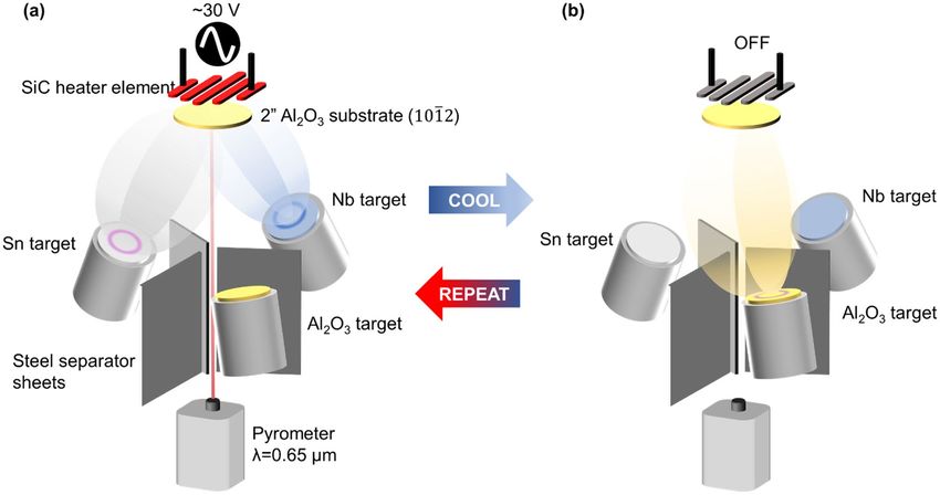
www.nature.com/scientificreports/
Figure 2. Connecting the Nb-Sn phase diagram to electrical properties and process window. (a) Relevant
adsorption-controlled growth regime (orange) of Nb-Sn phase diagram. Nb3Sn spans 17–25% Sn, and the
desired Nb3Sn + liquid Sn field lies above 930 °C and 25% Sn. (b) Tc, ΔTc, vs the Sn flux of 60 nm thick Nb3Sn
single layer thin films on Al2O3 substrates. T
c levels off above 1.0 Å/s Sn, corresponding to the adsorption-
controlled growth window and the film composition reach 25% Sn.
material into the two-phase region, where excess Sn re-evaporates from the film, avoiding the formation of Sn
precipitates23,24. To achieve the high temperatures (> 930 °C) required for this growth, sapphire substrates were
heated from behind with a SiC radiative heater. Radiation passed through the substrate and heated the deposit-
ing metal directly. Growth temperature was measured by pyrometer. Details of the film growth are given in the
Supplemental Information.
A series of films was grown with fixed Nb flux (0.7 Å/s) and varying Sn flux (0.4–2.5 Å/s), and low-tempera-
ture resistance measurements were carried out to find the window for this self-regulating adsorption-controlled
process. Shown in Fig. 2b are the dependencies of the critical temperature Tc and transition width ΔTc on the
deposition rate of Sn which clearly saturate at ~ 1 Å/s. Given the dependence of Tc on Sn content in Nb3Sn, this
growth rate roughly corresponds to the boundary between two processing regimes. At lower flux, Sn evaporates
from the film faster than it can be incorporated, resulting in a Sn-deficient film. At higher flux, sufficient Sn is
provided to react with all available Nb, and only excess Sn re-evaporates.
The dielectric A l2O3 interlayers were grown after allowing N b3Sn to cool down to < 400 °C, using a single
stoichiometric target with RF power at a rate of 1.8 nm/min without any further heating applied to the substrate.
Depositing under these conditions protects the SiC heater element from oxygen evolved during the sputtering
process and prevents undesired reactions with the N b3Sn surface. This N
b3Sn/Al2O3 stack was then heated again
to above 900 °C, which allows the A l2O3 to crystallize, and the process was repeated to grow heterostructures of
up to three N
b3Sn layers. The chamber setup and growth steps are depicted in Fig. 3.
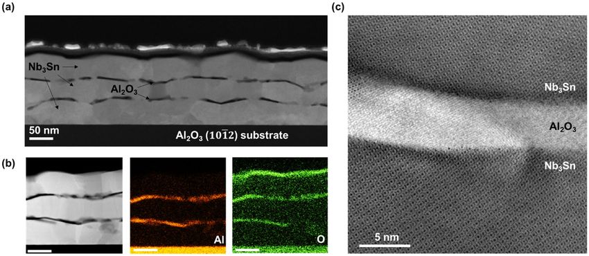
Structural characterization. A SIS sample with three Nb3Sn layers was prepared for analysis by cross-
sectional scanning transmission electron microscopy (STEM). A low-magnification image (Fig. 4a) represents
the morphology and nanostructure of the stack. Each N b3Sn layer is polycrystalline with irregular interfaces and
grain size is 20–100 nm along the film surface direction. The Al2O3 layers conform closely to the layer below
but are discontinuous along the N b3Sn/Al2O3 interface. Despite the repeated thermal cycling during stacking, it
appears that the lower layers have not degraded in comparison to the top layer.
The chemical stability of these films is further confirmed by compositional mapping with energy dispersive
spectroscopy (EDS) (Fig. 4b). Intensity of the Al Kα and O Kα peaks are mapped from the region shown on the
left. Although the Al2O3 layers are not continuous, Al and O are confined to the Al2O3 layers, and do not mix with
the Nb3Sn layers. The exception to this is the presence of O at the interface of the topmost Nb3Sn film with the
atmosphere, where ambient conditions are sufficient to cause a reaction. A capping Al2O3 layer could be deposited
Scientific Reports | (2021) 11:7770 | https://doi.org/10.1038/s41598-021-87119-9 3
Vol.:(0123456789)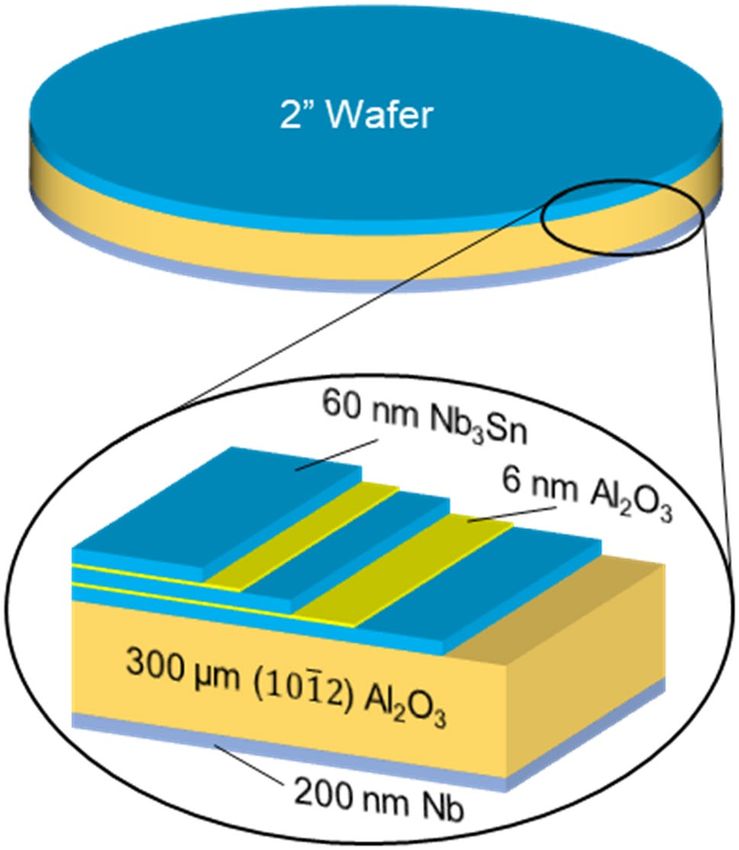
www.nature.com/scientificreports/
Figure 3. Schematic of thin films deposition setup and sequential processing steps for N b3Sn/Al2O3 multilayer
heterostructures. (a) Nb and Sn are sputtered onto A l2O3 substrate while heater element is powered on. (b) After
allowing film to cool, A
l2O3 is sputtered from a single stoichiometric Al2O3 target. Sample is heated again to
anneal Al2O3. These two steps are repeated to produce multilayer samples.
Figure 4. Cross-sectional transmission electron microscopy images of Nb3Sn/Al2O3 multilayer heterostructures
(a) Low-magnification image of trilayer morphology. (b) EDS compositional mapping of Al and O showing no
interdiffusion between Al2O3 and Nb3Sn. (c) High-magnification image of the interfaces between Al2O3 and
Nb3Sn.
to prevent this oxidation, but we did not use it for the multilayer samples described in this work. Note that the
slight O signal in the Nb3Sn layers in Fig. 4b are due to the slight oxidation of the TEM specimen surface. As our
RF cavity measurements show, these Al2O3 layers do not contribute significantly to surface resistance at low fields.
A higher-magnification image of the S–I interface is shown in Fig. 4c. The atomic structure of N b3Sn is well-
preserved at the interface, suggesting that there is almost no diffusion or intermixing from the A l2O3. The lower
Nb3Sn grain orients the [023] direction normal to the film surface, and this direction is also preserved in the
upper Nb3Sn grain. This can occur when the upper N b3Sn layer deposits with the same epitaxial relationship to
the underlying A l2O3 as the lower layer has with the A
l2O3 substrate. This structure can also form when a N b3Sn
Scientific Reports | (2021) 11:7770 | https://doi.org/10.1038/s41598-021-87119-9 4
Vol:.(1234567890)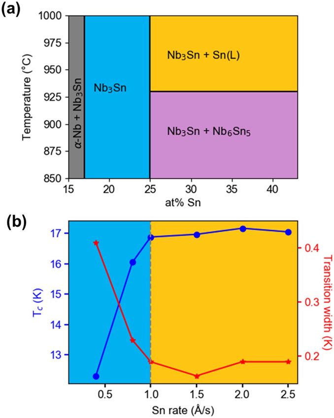
www.nature.com/scientificreports/
Figure 5. Superconducting properties of single-layer Nb3Sn films. (a) Resistive superconducting transition
for two identical 60 nm thick films, one of which is capped with 6 nm A l2O3 overlayer and annealed at 900 °C
for 10 min. (b) Density of states measured by scanning tunneling spectroscopy and Dynes fit for a 60 nm thick
Nb3Sn film.
grain nucleates on top of a N b3Sn surface exposed by breaks in the discontinuous A
l2O3 layer. X-ray diffractom-
etry indicates that N b3Sn grains in the second layer have more random crystallographic orientation compared
to the first layer (see the Supplemental material).
Superconducting properties. Our dc transport measurements have shown that the Nb3Sn films capped
with Al2O3 and annealed with no further deposition exhibit good superconducting properties. For instance, the
superconducting resistive transitions of a bare Nb3Sn film and a Nb3Sn/Al2O3 structure annealed at 900 °C for
10 min are shown in Fig. 5a. Here the critical temperature of the annealed sample is about 0.25 K higher than Tc
of the unannealed sample, and residual resistivity ratio (RRR), an indicator of crystalline and metallic quality, is
improved from 3.5 to 4.26. On the other hand, N b3Sn films annealed without the Al2O3 cap, even under high Sn
flux to prevent evaporative loss, have degraded superconducting properties compared to an un-annealed film.
The superconducting properties essential for the RF performance were characterized by scanning tunneling
spectroscopy (STS) which measures the differential tunneling conductance dI/dV proportional to the quasi-
particle density of states (DOS), N(E). Shown in Fig. 5b is a representative tunneling spectrum measured in the
center of a Nb3Sn grain at 4 K. The DOS curves, which clearly show the superconducting gap at the Fermi
surface, were fit using the conventional Dynes model25,26:
E − iŴ
N(E) = N0 Re
(1)
(E − iŴ)2 − �2
where the phenomenological parameter Γ accounts for the broadening of the DOS peaks due to a finite lifetime
of quasiparticles, and N0 is the DOS in the normal state. The fit was done with Γ = 0.4 meV and ≈ 3.1 meV,
consistent with the conventional gap value for a stoichiometric Nb3Sn4. The ratio Ŵ/� ≈ 13% in our samples
turns out to be about 2–3 times larger than the values observed by tunneling spectroscopy on 1–2 μm thick
Scientific Reports | (2021) 11:7770 | https://doi.org/10.1038/s41598-021-87119-9 5
Vol.:(0123456789)www.nature.com/scientificreports/
Figure 6. (a) Cutaway of hemispherical resonator cavity at SLAC used for these measurements. RF power is
pumped in at the bottom, and magnetic field lines oscillate parallel to sample surface. (b) RF Surface resistance
measurements of N b3Sn film and multilayer compared to cavity-grade Nb.
Nb3Sn films for rf a pplications27 and Nb coupons28. The deviations of the STM data from the Dynes model at
low energies E < � may indicate the effects of local non-stoichiometry, gap anisotropy and s train22, scattering
of quasiparticles on magnetic impurities, and a thin layer with deteriorated superconducting properties at the
surface27–30. In turn, the subgap quasiparticles states which appear at |E|< Δ due to a finite Γ contribute to a
temperature-independent residual surface resistance Ri at kBTwww.nature.com/scientificreports/
ing to simulations, the participation factor is 0.33 for the 2″-diameter sample. Crucially, the magnetic field at the
sample is in the radial direction and parallel to the sample surface, making it possible to measure RF properties
of the sample without interference from the perpendicular component of the field. Low-field measurements of
Q(T) of a N
b3Sn film in an uncoated Cu cavity are presented in the Supplementary Information.
The SRF performance of two Nb3Sn samples were compared in this system to a cavity-grade bulk Nb coupon.
A 500 nm (~ 4λ) Nb3Sn film intended to completely screen out the RF magnetic field, and a 3 × 60 nm N b3Sn/
Al2O3 trilayer were tested under the RF field. Both samples were coated with a 200 nm Nb film on the backside
of the wafer to prevent leakage of magnetic field as shown in Fig. 1. The quality factor of the cavity with each
sample, measured at low power with a network analyzer, is plotted in Fig. 6b. The abrupt increase in Q at about
15 K corresponds to the superconducting transition of Nb3Sn, followed by an increase of Q(T) at Tc = 9 K of the
Nb-coated host cavity.
As shown in Fig. 6b, the thick Nb3Sn film and the trilayer have nearly identical Q at T < 9 K, indicating that
Al2O3 dielectric layers and interfaces do not contribute significantly to the RF dissipation. We would expect the
thick Nb3Sn film to have a higher Q, as magnetic field is more fully screened before reaching the substrate and
backside, so this result suggests that the maximum Q of these films and multilayers is limited by the quality of the
Nb3Sn material rather than by the interfaces with A l2O3. The quality factors of both the film and the trilayer sam-
ples exceed Q(T) of Nb at T > 6 K due to the higher Tc of N b3Sn and is about 2 times smaller than Q of Nb at 4 K.
Discussion. The results of this work show that, despite the obvious non-stoichiometry and inhomogeneity
of superconducting properties, grain boundaries, Nb inclusions, and incomplete A l2O3 layers, our multilayers
exhibit the quality factors on par of those of cavity-grade bulk Nb at 4 K and low RF power. The significant
local non-stoichiometry of thick (a few micron) polycrystalline Nb3Sn coatings of Nb c avities20,27, as well as
Sn depletion at grain boundaries in N b3Sn34–37 have been well documented in the literature. Yet, despite these
materials issues which are also characteristic of 1–3 μm thick Nb3Sn films used in SRF cavities38, our Nb3Sn SIS
structures exhibit higher low-field Q values than Nb at T > 6 K20, consistent with the larger superconducting
1/2
energy gap Nb3Sn ≈ 2 Nb and a lower BCS surface resistance RBCS ∝ ω2 ρn e−�/kB T of Nb3Sn. These experi-
mental results not only show a remarkable resilience of low-field quality factors of N b3Sn to the significant non-
stoichiometry and materials imperfections but also suggest that the SRF performance of N b3Sn coatings can be
further improved by materials treatments. Our N b3Sn multilayers exhibit a similar resilience of the low-power
SRF performance to the materials imperfections.
The slopes of Q(T) for both the N b3Sn film and multilayer shown in Fig. 5 tend to level off at 4–5 K and are
clearly smaller than the slope of Q(T) for Nb. This indicates that Q(T) of the N b3Sn samples at T = 4–5 K is not
limited by the BCS surface resistance for which the slope of Q(T) ∝ e�/kB T for N b3Sn would be larger than for
Nb because Nb3Sn ≈ 2 Nb . The behavior of Q(T) of the N b3Sn samples at 4–5 K is thus indicative of a sig-
nificant residual surface resistance caused by the multiphase structure of the films and multilayers and trapped
vortices. Yet Q0 ≃ 107 observed on our Nb3Sn multilayers at 11.4 GHz and 4 K suggests values of Q0 ∼ 109 at
4 K and 1 GHz given the frequency dependence Q ∝ ω−2 which comes from the BCS surface r esistance1–3,
ohmic losses in metallic precipitates smaller than the RF skin depth and perhaps Josephson vortices trapped on
grain boundaries39.
SRF performance at high RF fields and breakdown fields of Nb3Sn/Al2O3 multilayers are yet to be explored.
Generally, the effects of nonstoichiometry, proximity-coupled normal precipitates and weakly-coupled grain
boundaries become more pronounced at higher RF fields. For instance, nonstoichiometric grain boundaries in
Nb3Sn have been identified as prime pinning centers for vortices in Nb3Sn wires for high-field dc m agnets39.
However, weakly-coupled grain boundaries in Nb3Sn coating layers would block RF currents and cause dis-
sipative penetration of Josephson vortices at fields well below the superheating fi eld40, and sub-stoichiometric
regions in Nb3Sn-coated Nb cavities are suspected to play an important role in RF cavity quench27. At the same
time, meandering and breaks in Al2O3 layers shown in Fig. 4 may not be detrimental for SRF performance as
the layers can still provide their main role of intercepting and pinning small vortex loops originating at surface
structural defects5,8 since the pinholes sizes 10–50 nm in the Al2O3 layers are smaller than magnetic size of the
vortex ≃ 100−200 nm of N b3Sn. The misaligned breaks with lateral sizes smaller than the N b3Sn layer thick-
ness in neighboring dielectric Al2O3 layers are not expected to strongly deteriorate the SRF performance of
multilayers. Such imperfect dielectric layers still produce effective pinning barriers against penetration of parallel
vortices and arresting vortex semi-loops originating on surface materials defects, which is instrumental in the
multilayer approach5,6. At the same time, the roughness and breaks in Al2O3 interlayers, as well as the variable
thickness of N b3Sn layers can pin short perpendicular vortices and do not let them propagate along the layers
under RF current, which is also beneficial for the SRF performance of m ultilayers5. Though A l2O3 layers do not
fully separate Nb3Sn layers, we found that a 500 nm thick Nb3Sn film had a quality factor identical to a multilayer
with three 60 nm Nb3Sn layers separated by 6 nm A l2O3, and both had Q approximately 2 times lower than a
cavity-grade Nb reference. This indicates that losses in the thin A l2O3 and the oxide-metallic interfaces do not
contribute much to the surface resistance of our multilayer samples.
Conclusions
In summary, we have developed a self-regulating, adsorption-controlled process for growth of N b3Sn films and
Nb3Sn/Al2O3 multilayers. We have produced and characterized multiple multilayer samples with up to four
superconducting layers. Despite the detrimental effects of nonstoichiometry, grain boundaries and breaks in
the meandering A l2O3 interlayers, the SRF performance of our multilayers turned out to be on par with that of
Nb films. The growth technique reported in this work provides a platform for further optimizations of the SRF
properties of SIS high-performance multilayers for superconducting resonator applications.
Scientific Reports | (2021) 11:7770 | https://doi.org/10.1038/s41598-021-87119-9 7
Vol.:(0123456789)www.nature.com/scientificreports/
Methods
Film deposition was carried out in a vacuum chamber pumped down to 3.0 × 10⁻⁸ Torr before being backfilled
with Ar. N b3Sn films were sputtered from elemental Nb (99.95%) and Sn (99.99%) targets in 3 mTorr of Ar to
maximize deposition rate, at a distance of 15.5 cm from the substrate to improve flux uniformity. DC power to
the sputter guns was current-controlled, and deposition rate was measured with an in situ quartz crystal monitor
prior to growth. Pyrometer reading of the SiC heating element at the beginning of growth was ~ 1250 °C, and
dropped to around 905 °C after 60 nm was deposited. A l2O3 was sputtered from a stoichiometric 2″ diameter
ceramic target after the pyrometer reading fell below 400 °C. After deposition, the temperature was ramped
back up to a pyrometer reading of 905 °C over the course of 10 min. These two steps were repeated to produce
the multilayers.
Scanning transmission electron microscope (STEM) imaging and elemental analysis were performed in
a probe-corrected atomic resolution analytical electron microscope (JEM-ARM200cF, JEOL) with an energy
dispersive X-ray spectroscopy (EDS) detector (X-MaxN 100TLE SDD, Oxford Instruments).
Superconducting transitions were measured in a closed-loop He cooler using 4-point van der Pauw geometry
on 10 × 10 mm samples. The critical temperature Tc is defined as the temperature at which the sheet resistance
falls below 1% of its normal state value at 18 K. The transition width ΔTc is defined as a difference between Tc and
the point at which the lines drawn through the normal-state resistance and transition region intersect.
Low-temperature scanning tunneling microscopy/spectroscopy (STM/S) measurements were carried out in
a STM system (USM1300, UNISOKU) at 4 K using polycrystalline PtIr tips. The dI/dV spectra were acquired
using standard lock-in technique by applying a bias modulation of 0.2 mV (r.m.s.) at 732 Hz.
Data availability
The data that supports the findings of the work are in the manuscripts main text and Supplementary Information.
Additional data are available from the corresponding author upon reasonable request.
Received: 20 January 2021; Accepted: 15 March 2021
References
1. Padamsee, H., Knobloch, J. & Hays, T. RF Superconductivity for Accelerators (Wiley, 2008).
2. Gurevich, A. Superconducting radio-frequency fundamentals for particle accelerators. Rev. Accel. Sci. Technol. 05, 119–146 (2012).
3. Padamsee, H. S. Superconducting radio-frequency cavities. Annu. Rev. Nucl. Part. Sci. 64, 175–196 (2014).
4. Valente-Feliciano, A.-M. Superconducting RF materials other than bulk niobium: A review. Supercond. Sci. Technol. 29, 113002
(2016).
5. Gurevich, A. Theory of RF superconductivity for resonant cavities. Supercond. Sci. Technol. 30, 034004 (2017).
6. Gurevich, A. Enhancement of rf breakdown field of superconductors by multilayer coating. Appl. Phys. Lett. 88, 012511 (2006).
7. Kubo, T., Iwashita, Y. & Saeki, T. Radio-frequency electromagnetic field and vortex penetration in multilayered superconductors.
Appl. Phys. Lett. 104, 032603 (2014).
8. Gurevich, A. Maximum screening fields of superconducting multilayer structures. AIP Adv. 5, 017112 (2015).
9. Liarte, D. B. et al. Theoretical estimates of maximum fields in superconducting resonant radio frequency cavities: Stability theory,
disorder, and laminates. Supercond. Sci. Technol. 30, 033002 (2017).
10. Kubo, T. Multilayer coating for higher accelerating fields in superconducting radio-frequency cavities: A review of theoretical
aspects. Supercond. Sci. Technol. 30, 023001 (2017).
11. Antoine, C. Z. et al. Characterization of superconducting nanometric multilayer samples for superconducting rf applications: First
evidence of magnetic screening effect. Phys. Rev. Spec. Top. Accel. Beams 13, 121001 (2010).
12. Tajima, T. et al. Studies on thin film MgB2 for applications to RF structures for particle accelerators. AIP Conf. Proc. 1435, 297–304
(2012).
13. Antoine, C. Z., Villegier, J.-C. & Martinet, G. Study of nanometric superconducting multilayers for RF field screening applications.
Appl. Phys. Lett. 102, 102603 (2013).
14. Beringer, D. B. et al. Thickness dependence and enhancement of H c1 in epitaxial MgB2 thin films. IEEE Trans. Appl. Supercond.
23, 7500604–7500604 (2013).
15. Roach, W. M., Beringer, D. B., Li, Z., Clavero, C. & Lukaszew, R. A. Magnetic shielding larger than the lower critical field of niobium
in multilayers. IEEE Trans. Appl. Supercond. 23, 8600203–8600203 (2013).
16. Tan, T. et al. Enhancement of lower critical field by reducing the thickness of epitaxial and polycrystalline M gB2 thin films. APL
Mater. 3, 041101 (2015).
17. Tan, T., Wolak, M. A., Xi, X. X., Tajima, T. & Civale, L. Magnesium diboride coated bulk niobium: A new approach to higher
acceleration gradient. Sci. Rep. 6, 35879 (2016).
18. Junginger, T., Wasserman, W. & Laxdal, R. E. Superheating in coated niobium. Supercond. Sci. Technol. 30, 125012 (2017).
19. Antoine, C. Z. et al. Optimization of tailored multilayer superconductors for RF application and protection against premature
vortex penetration. Supercond. Sci. Technol. 32, 085005 (2019).
20. Posen, S. & Hall, D. L. Nb3Sn superconducting radiofrequency cavities: Fabrication, results, properties, and prospects. Supercond.
Sci. Technol. 30, 033004 (2017).
21. Charlesworth, J. P., Macphail, I. & Madsen, P. E. Experimental work on the niobium-tin constitution diagram and related studies.
J. Mater. Sci. 5, 580–603 (1970).
22. Godeke, A. A review of the properties of N b3Sn and their variation with A15 composition, morphology and strain state. Supercond.
Sci. Technol. 19, R68–R80 (2006).
23. Allen, L. H., Anklam, W., Beasley, M. R., Hammond, R. H. & Turneaure, J. P. RF surface resistance in Nb3Sn thin films. IEEE Trans.
Magn. 21, 525–527 (1985).
24. Allen, L. H., Beasley, M. R., Hammond, R. H. & Turneaure, J. P. RF Surface resistance of Nb3Sn, NbZr, and NbN thin films. IEEE
Trans. Magn. 23, 1405–1408 (1987).
25. Dynes, R. C., Narayanamurti, V. & Garno, J. P. Direct measurement of quasiparticle-lifetime broadening in a strong-coupled
superconductor. Phys. Rev. Lett. 41, 1509–1512 (1978).
26. Dynes, R. C., Garno, J. P., Hertel, G. B. & Orlando, T. P. Tunneling study of superconductivity near the metal-insulator transition.
Phys. Rev. Lett. 53, 2437–2440 (1984).
Scientific Reports | (2021) 11:7770 | https://doi.org/10.1038/s41598-021-87119-9 8
Vol:.(1234567890)www.nature.com/scientificreports/
27. Becker, C. et al. Analysis of Nb3Sn surface layers for superconducting radio frequency cavity applications. Appl. Phys. Lett. 106,
082602 (2015).
28. Lechner, E. M. et al. Electron tunneling and X-ray photoelectron spectroscopy studies of the superconducting properties of
nitrogen-doped niobium resonator cavities. Phys. Rev. Appl. 13, 044044 (2020).
29. Gurevich, A. & Kubo, T. Surface impedance and optimum surface resistance of a superconductor with an imperfect surface. Phys.
Rev. B 96, 184515 (2017).
30. Proslier, T. et al. Tunneling study of cavity grade Nb: Possible magnetic scattering at the surface. Appl. Phys. Lett. 92, 212505 (2008).
31. Visentin, B., Barthe, M. F., Moineau, V. & Desgardin, P. Involvement of hydrogen-vacancy complexes in the baking effect of niobium
cavities. Phys. Rev. Spec. Top. Accel. Beams 13, 052002 (2010).
32. Dhakal, P., Ciovati, G. & Gurevich, A. Flux expulsion in niobium superconducting radio-frequency cavities of different purity and
essential contributions to the flux sensitivity. Phys. Rev. Accel. Beams 23, 023102 (2020).
33. Welander, P., Franzi, M. & Tantawi, S. Cryogenic RF characterization of superconducting materials at SLAC with hemispherical
cavities. In Proceedings of SRF2015 735–738 (2015).
34. Suenaga, M. & Jansen, W. Chemical compositions at and near the grain boundaries in bronze-processed superconducting N b3Sn.
Appl. Phys. Lett. 43, 791–793 (1983).
35. Sandim, M. J. R. et al. Grain boundary segregation in a bronze-route N b3Sn superconducting wire studied by atom probe tomog-
raphy. Supercond. Sci. Technol. 26, 055008 (2013).
36. Lee, J. et al. Atomic-scale analyses of Nb3Sn on Nb prepared by vapor diffusion for superconducting radiofrequency cavity applica-
tions: A correlative study. Supercond. Sci. Technol. 32, 024001 (2019).
37. Lee, J. et al. Grain-boundary structure and segregation in N b3Sn coatings on Nb for high-performance superconducting radi-
ofrequency cavity applications. Acta Mater. 188, 155–165 (2020).
38. Spina, T., Tennis, B. M., Lee, J., Seidman, D. N. & Posen, S. Development and understanding of N b3Sn films for radiofrequency
applications through a sample-host 9-cell cavity. Supercond. Sci. Technol. 34, 015008 (2021).
39. Scanlan, R. M., Fietz, W. A. & Koch, E. F. Flux pinning centers in superconducting N b3Sn. J. Appl. Phys. 46, 2244–2249 (1975).
40. Sheikhzada, A. & Gurevich, A. Dynamic transition of vortices into phase slips and generation of vortex-antivortex pairs in thin
film Josephson junctions under dc and ac currents. Phys. Rev. B 95, 214507 (2017).
Acknowledgements
This work was supported by the US Department of Energy under grant # DE-SC0010081-020. Work at West
Virginia University was supported by the U.S. Department of Energy under Award # DE-SC0017632. Work
at SLAC National Accelerator Laboratory was supported by the U.S. Department of Energy under contract #
DE-AC02-76SF00515. The nanostructural characterizations were supported by the National High Magnetic Field
Laboratory and the National Science Foundation under grant # NSF/DMR-1644779), and by the State of Florida.
Author contributions
C.S. developed multilayer growth process and fabricated samples. J.M. participated in RF characterization.
Y.S., F.K., and L.X. performed cross-sectional TEM characterization. H.Z. and L.L. performed low-temperature
STM characterization. P.B.W. performed low-temperature RF surface resistance characterization. C.B.E and
A.G. initiated and directed the project. C.S and A.G. wrote the manuscript with contributions from all authors.
Competing interests
The authors declare no competing interests.
Additional information
Supplementary Information The online version contains supplementary material available at https://doi.org/
10.1038/s41598-021-87119-9.
Correspondence and requests for materials should be addressed to A.G. or C.-B.E.
Reprints and permissions information is available at www.nature.com/reprints.
Publisher’s note Springer Nature remains neutral with regard to jurisdictional claims in published maps and
institutional affiliations.
Open Access This article is licensed under a Creative Commons Attribution 4.0 International
License, which permits use, sharing, adaptation, distribution and reproduction in any medium or
format, as long as you give appropriate credit to the original author(s) and the source, provide a link to the
Creative Commons licence, and indicate if changes were made. The images or other third party material in this
article are included in the article’s Creative Commons licence, unless indicated otherwise in a credit line to the
material. If material is not included in the article’s Creative Commons licence and your intended use is not
permitted by statutory regulation or exceeds the permitted use, you will need to obtain permission directly from
the copyright holder. To view a copy of this licence, visit http://creativecommons.org/licenses/by/4.0/.
© The Author(s) 2021
Scientific Reports | (2021) 11:7770 | https://doi.org/10.1038/s41598-021-87119-9 9
Vol.:(0123456789)You can also read