Epson FPGA to ASIC Conversion
←
→
Page content transcription
If your browser does not render page correctly, please read the page content below
Epson FPGA to ASIC Conversion
   Introduction | Feature | Advantages/Benefits | Design Flow/Interface | Design
                                   Consideration

Introduction
Epson has a FPGA to ASIC flow tailored to your needs. Epson has ASIC to FPGA
conversion methodology with complete support for industries leading FPGA families. Epson
provides drop in replacement to major industrial FPGA resulting in fast turn-around time,
reduced die size, reduced power consumption & low unit cost.

Epson offers the ASIC design solutions using a choice of ASIC Technologies-Gate Array,
Embedded Array and Standard Cell. Epson offers a broad lineup of advanced packages to
meet your diverse packaging needs. Epson has expertise in handling complex designs. We
accommodate the needs of our customers without compromising the success of the
conversion process. We constantly upgrade our Tools & FPGA database in order to support
larger number of FPGAs for conversion.

Feature
   •   Proven Design Methodology
   •   Higher Integration
   •   Easily Migrated to a Gate Array or Embedded Array or Standard Cell ASICs
   •   Availability of wide range of standard IPs, Embedded memories, Flash and Analog cells
   •   Conversion of Complex designs
   •   Acceptance of popular format of netlist/vectors

           o   Proven Design Methodology

               Epson's ASIC offerings aim at providing the best overall solution thus
               enabling our customers to get products to market successfully. Epson has
               completed the FPGA to ASIC conversion from all leading FPGA vendors, we
               also have the mapped libraries of all the major FPGA/CPLD suppliers to
               enable efficient conversion. Using this methodology we have completed over
               100 FPGA to ASIC conversions. Epson offers wide range of device selection
               ranging from 2.8K to 10M gates. Industries leading EDA like Synopsys ,
               Cadence are supported in our design flow. We also support popular formats
               like VHDL, Verilog, EDIF & XNF in our design flow.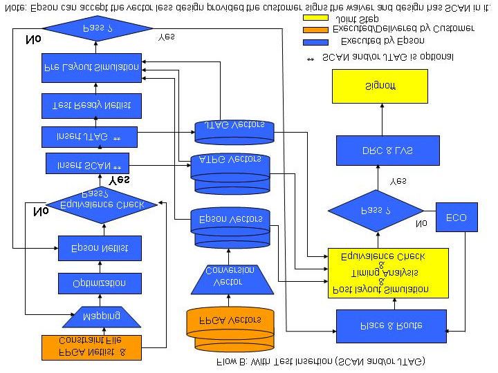
o   Higher Integration

    FPGAs require large number of gates for programming, this would result in a
    bigger die size. The ASICs do not require the programmability option
    resulting in a smaller die size. Our high density feature enables our customers
    to implement multiple FPGAs into a single ASIC resulting in optimal
    performance and reduced cost. Our Space Saving technology uses ultra-
    precise methods of processing and mounting to create a wide range of lighter,
    compact devices.

o   Easily Migrated to a Gate Array or Embedded Array or Standard Cell
    ASICs

    Using Epson's design flow, FPGAs can be easily migrated to a Gate Array or
    Embedded Array or Standard cell ASICs. Gate Arrays address the need for
    fast turn around time and low development costs. Standard Cells make system
    solutions possible at lowest unit cost. Embedded arrays combine the
    functionality of fast turn around time of gate arrays and the ability to
    implement system level functionality on the chip available with Standard Cell.

o   Availability of wide range of standard IPs, Embedded memories,
    Flash and Analog cells

    Macro Cells are indispensable elements for the development of LSI. The
    availability of wide selection of Standard IPs, macro cells, Analog Cells and
    memories help realize your complex SOC solution. We offer IPs necessary for
    the development of PC peripherals, Graphic chipsets, Mobile communication
    and Networking ASICs.

o   Conversion of Complex designs

    Epson has vast experience and successful track record of converting complex
    designs with certain or combined characteristic such as large gate count, bus
    count, I/O count, sizeable and various configured memory, gated clock
    scheme, multiple clock domains (synchronous and/or asynchronous), and
    aggressive timing constraints.

o   Acceptance of popular format of netlist/vectors

    With our highly experienced engineering staff and large FPGA database,
    Epson can handle netlist in various format, such as Verilog, EDIF, VHDL and
    XNF, to support most major FPGA vendors and families. If behavioral or
    RTL code and design constraint s were given, Epson will provide expert
    service to synthesize the code to structural level and generate mapped gate-
    level netlist for layout and simulation. It is important that customer can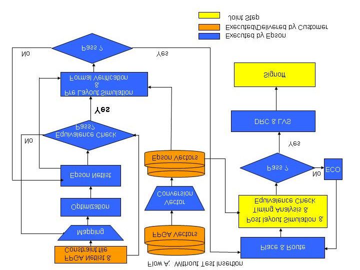
provide special cells and other critical design information at early stage of
              design process so that correct conversion measures can be taken to prevent
              schedule delay. Regarding test vectors Epson accepts either print on change
              format from any simulation environment or self checking verilog test benches
              that check all the inputs and outputs during simulation. As our experience
              grows with more design completion, Epson is capable of constantly adding
              new types of input vector format to its support list.

Advantages/Benefits
 •   Lower unit cost
 •   Lower power consumption
 •   Extensive package choices
 •   Better performance
 •   Flexible clock
 •   Drop-in replacement
 •   Availability and lifetime consideration

         o    Lower unit cost (Smaller die, Lower pin count package, Higher
              density)

              In most cases, an ASIC die will be smaller and cost less than a comparable
              FPGA die. The programming flexibility of the FPGA architecture requires
              more silicon area to implement a logic function than in an ASIC, which adds
              to the FPGA's higher cost.
              When a design has a high gate count, but low I/O count, a large FPGA
              package configuration will be used. Additional cost savings can be realized
              becasue the ASIC is placed in a smaller package.
              Even though ASICs do have nonrecurring engineering (NRE) costs, the cost
              can be recovered in the unit-cost savings if you have large volumes in
              production. The annual volume at which the NRE costs are recovered and
              overall cost savings are realized can be as little as 1,000 units for complex
              FPGAs. Wafer costs for an FPGA are also typically higher because of the
              masking levels required for programmable logic architectures.

         o    Lower power consumption

              ASIC devices implement fully optimized interconnect, resulting in power
              consumption which is an order of magnitude lower than FPGAs. As a general
              guideline, design implemented in an FPGA consumes roughtly three times the
              power of the same design implemented in ASIC technology. Epson offers
              power consumption as low as 0.049 uW/Mhz/gate, Epson also offers dual
              power supply interfaces using level shifters & fail safe I/O buffers.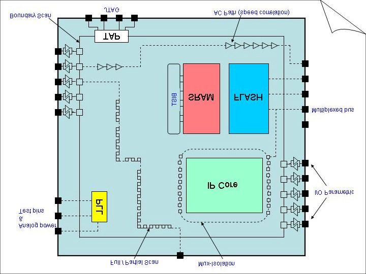
o   Extensive package choices

    Given the trend toward ever advancing compact electronic devices, packaging
    technologies for high density implementation of highly integrated, high speed
    ASICs have become increasingly important.Consequently, Epson provides a
    broad lineup of packages to meet customer's diverse packaging needs for
    chips with widerange of lead counts and geometries. We also offer advanced
    packaging technology and diverse type of packages ranging from QFP, CSP,
    BGA, etc. Epson offers Dimensional Compatibility matching your FPGA
    footprint. Epson also offers non-pin compatible solutions for ASICs that
    require less power and ground pins than the FPGAs.

o   Design functionality will be maintained and performance will be
    improved

    During conversion to an ASIC, all programmable interconnect structures are
    removed and the best possible performance is attained. And the functionality
    will be maintained.

o   Flexible clock handling scheme

    While clock distribution is normally not a serious concern of the designer, it's
    smart to be aware of the differences between FPGA and ASIC clock
    distribution issues.
    Clock distribution issues apply to any signal with large loads that must be
    switched with minimal skew or differential delay. In most cases, the
    maximum clock skew must be less than the flip- flop hold-time requirement.
    FPGA architectures typically support a limited number of predesigned clock
    trees designed to drive a fixed set of flip-flop clock pins. ASICs, on the other
    hand, support any number of clocks with clock tree synthesis. Each clock tree
    is synthesized to drive a specific set of flip- flops. This gives the best
    performance with minimal skew and power consumption.

o   Drop-in replacement

    FPGA consumers scrambling to find replacement parts. Often it's hard to find
    a part with the same package and pinout, especially with respect to power and
    ground connections. ASIC migration services can address these problems by
    providing drop-in replacement parts.

o   Device availability and product lifetime consideration

    The fast FPGA parts are often very hard to obtain because of either processing
    problems or high demand, and are often reserved for key customers. ASICs
    are built to a performance spec and all the parts work to that spec.
Once your design is complete, you may need to be able to buy the same part for many years. Unfortunately, in the race to advance FPGA technology, vendors are migrating or obsoleting older products at an accelerated rate. ASIC vendors support old ASIC manufacturing process recipes for years by adapting the old process flows to new equipment.
Design Flow/Interface
 •   Epson design flow
 •   Deliverable & Responsibility
 •   Supported tools

         o   Epson design flow

                 §    Without Test insertion
• With Test insertion
o Deliverable & Responsibility
§ Task Responsibility
Task Responsibility Customer Epson
Design consultation & specification √
Behavioral coding / RTL validation √
Netlist mapping / synthesis √
Functional simulation √
Layout / P & R √
Timing analysis & closure √ √
DFT & vector generation √
Project review & signoff √ √
Fabrication – assembly – testing √
Prototype evaluation & approval √· Example Design Flow
FPGA to ASIC conversion project work flow
Customer Milestone Epson
RFQ
Identify / provide conversion Deliverable check, conversion
1 source material & target feasibility study
specification
Feasibility check
passed, Contract, PO
Provide final RTL / netlist, Design re-target, stimulus to
2 timing constraints, functional vector conversion, optional scan
stimulus / JTAG insertion
Preliminary verification
(simulation, timing analysis)
Functional simulation and timing Provide converted netlist,
3 check verification reports, library kit
Pre-layout check
passed
P&R
Post-layout simulation & timing SDF generation
check
Post layout verification
4
Report timing issue or fix (if Fix timing violations (if
necessary) necessary)
P&R ECO (if necessary)
Timing closure
Provide & authorize signoff Prepare signoff, optional ATPG,
5 documentation final vector qualification
Final Signoff
Layout verification
Mask generation
Fabrication
Wafer sort & cut
Assembly & Testing
6 ES evaluation ES delivery§ Deliverable Responsibility
Deliverable FPGA I/F
Design / system specification
FPGA netlist (if not RTL)
Customer
RTL source code (if not netlist)
Synthesis constraint / script
Function simulation pattern
Simulated Epson netlist &
vector
Pinout assignment
Library, Model, datasheet
Simulated netlist
Epson
Simulation & timing report
Test vector & coverage
Layout RC-delay & tape
Prototype
§ Issue and Handling
Common Issue FPGA ASIC Common Handling
Logic utilization & Logic Gate (Cell) - Sizing assumed LE fully utilized
sizing Element (LE) - Sizing based on re-mapping
Clock generation & Built-in Embedded - User accepts Epson PLL spec.
phase control DLL / PLL (or GA) - User adds PLL test pins
PLL
I/O interface Configurable Fixed I/O - User selects available I/O from
I/O Epson Library
IP block testing User User - User adds access circuitry / pin
don’t_care integrated - Factory provides qualified vector
Fault coverage User User - User adds DFT (e.g. SCAN)
don’t_care determined - User / Factory recommends fault
detection level§ Check List
Please print out the Check List and fill as much information as
possible.
o Supported tools
Here are the tools supported by EEA
Physical Design Physical
Logic Design for
Vendor Synthesis (Place and Verification
Simulation Test
Route) DRC/LVS
Silicon
Verilog-XL
Ensemble-Ultra
Silicon
NC-Verilog
Build Ensemble-PKS
Cadence Verifault Dracula
Gates* Gate Ensemble-
Ultra
Signalscan
HLD-Floor
Planner
DFT
Compiler
Test Floorplan
Synopsys DC Expert PrimeTime Compiler Manager --
Tetramax (LBO/IPO)
BSD
Compiler
Modelsim
ModelTech -- VHDL -- -- --
Simulator
Novas -- Debussy -- -- --
Exemplar Leonardo -- -- -- --
DelayStorm
Simplex -- (delay -- -- --
calculator)
Memory
LogicVision -- -- -- --
BIST
*: Available but not officially supported.Design Consideration
• General DFT concept
• Scan/ATPG
• Design Initialization
• RAM Initialization
• Vectors
• JTAG
• Memory
• Clocks
• PLL
• Design Do's and Don'ts
o General DFT concept
§ ASIC Test Methodology§ Test Plan
Test Item Description Procedure
I/O Parametric Test I/O buffer (pad cell) • User to design pin out with pad cell
voltage & current parametric selection from library
• Epson to test pad cell per pin
assignment & pad specification
Functional Test user logic function based • User to supply simulation patterns
(User selective) on supplied patterns • Epson to verify & format vectors
(non-exhaustive)
Functional Test scan structured • User to request scan mode
(Scan based) sequential & combinatorial (provide chip resource as needed)
logic using ATPG • Epson to insert scan & run ATPG
AC path Test speed correlation by • Epson to insert and simulate delay
measuring AC path delay chain
against simulation
IDDQ Test device current leakage • Epson to select IDDQ cycle from
based on chip contents user supplied pattern (user to
design proper standby mode as
needed)
Memory Test memory block by one of MBIST*
following methods • Epson to insert MBIST circuitry
• MBIST • Epson to generate signature test
• Mux-isolation pattern
• Functional Read / Write Mux-isolation*
• Epson to insert multiplexing collar
around RAM macro I/O terminals
for parallel pin level access
• Epson to make factory test pattern
for RAM macro
Functional Read / Write
• User to provide function pattern to
exercise RAM contents (coverage
determined by user, detection not
guaranteed by Epson)
*Note: User to provide chip resource as
needed
PLL Test parametric and function • User to provide
of PLL macro - analog VDD & VSS
- dedicated test pins
(location recommended by Epson)
• User to identify signal pins for
multiplexing purpose if needed
• Epson to insert test circuitry around
PLL for pin level access
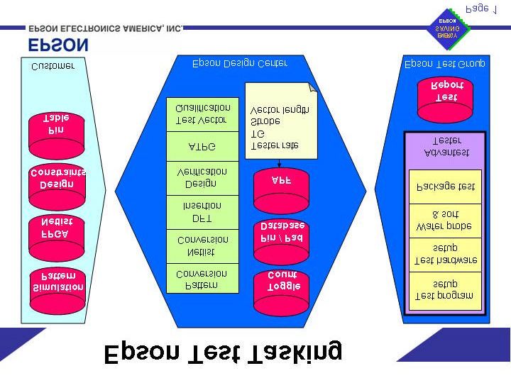
• Epson to make test program of PLL§ Epson Test Tasking
o Scan/ATPG
1. Introduction
What is SCAN and ATPG and why it is needed?
SCAN is a process of making sequential cells in the design controllable and
observable. Getting the functionality of the chip correct should not be the only
concern of the designer. It is equally important to detect any manufacturing
defects. To achieve this, it is important to have the test vectors which can
detect these problems. Once SCAN is inserted in the design, the ATPG tools
can be used to automatically generate the SCAN test vectors or ATPG vectors,
which will provide high coverage. ATPG stands for Automatic Test Pattern
Generation.
2. Manufacturing Defects
Manufacturing defects can be classified as
A. Defective Driver: Internal malfunction can make the output of the driver
to be permanently high or low.
B. Shorted Signal: A signal can be short-circuited to power or ground rail tobe permanently high or low.
C. Open Connection: A cut in the signal line can make it float to high or low.
Most of the above mentioned manufacturing defects can be represented as a
simple "stuck-at-0" (SA0) or "stuck-at-1" (SA1) fault.
3. Controllability / Observability
The node of a stuck-at fault must be controllable and observable for the fault
to be detected.
3.1 Controllable
A node is controllable if you can drive it to a specified logic value by
setting primary inputs to specific values, either directly or by the scan
operation.
3.2 Observable
A node is observable if you can predict the response on it and you can
propagate the response to primary outputs, where you can measure the
response either directly or by the scan operation.
4. Scan Techniques
For combinational circuits, it is relatively easy to get high fault coverage.
Sequential circuits are much more difficult since the tool needs to generate a
complex set of vectors applied in a particular order. To do this DFT (Design
For Test) strategy is used. Most popular DFT technique is SCAN insertion.
4.1 Full Scan
In the full- scan methodology, all sequential cells in the design are
modified to perform a serial shift function.
4.2 Partial Scan
In the partial-scan methodology, some of the sequential cells in the
design are made scannable. The selection of cells is based on
performance, area, and fault coverage constraints. ATPG process for a
partial-scan design is more complex and time-consuming than for a
full-scan design. EEA prefers customers to use full scan methodology
for their designs unless the customer is severely constrained with area
and timing requirements.
5. Scan Test Pins
For Scan Insertion, at least two extra primary input pins "test_mode" and
"test_scan_enable" are needed. The "test_mode" pin is needed for
multiplexing the internally generated clocks and primary clock inputs and to
disable internally generated asynchronous reset and set signals during scan
mode. The "test_scan_enable" pins is needed for enabling the scan chains.
Also, if another (optional) primary input pin "test_clock" is provided, this pin
can be used as a test clock in scan mode. Existing functional input and output
pins can be multiplexed and used as scan_in and scan_out test pins during
scan mode.
6. Scan Design Rules
1. Include all flip- flops in the scan path.2. The Set and Reset pins of the scannable flip- flop must be controllable
during the scan testing. In other words, the Set and Reset pins must be
controllable from external pins and held inactive during the scan test.
3. Multiple scan chains are allowed, with the following restrictions: Each
chain should use one clock, and all flip-flops must be driven by the
rising edge of the clock. The clock signal path should be laid out using
clock tree synthesis.
4. The test_mode signal should enable the 3-state control for all 3-state
I/O cells during scan test.
5. All megacells, RAM and ROM blocks must be disabled by test_mode.
6. If the design uses an internally generated clock (such as from a PLL),
and this clock drives flip- flops, disable the clock generator using a
MUX with Test_mode as the control, and insert a delay cell to
compensate for the delay.
7. Limit the scan chain to a length of about 500 to 1000 elements.
8. If multiple system clocks are used in the design, make sure the clocks
are not mixed in the same scan chain. Use only one clock per scan
chain.
9. Internal 3-state buffers should not be used
10. Post-layout simulation must be done with the ATPG vectors by
including the SDF file from the layout. At least, the scan chain
integrity check *_schk must pass the simulation with no mismatches or
timing errors. If Scan Insertion and/or ATPG generation is done by
EEA, then these simulations will be run by EEA. Also, If the number
of scan chains and length of scan chain is large for a high gate count
design, then there would be large number of ATPG vectors generated
(ranging from 1M events to 5M events for >1M gate count design.
Hence, please allow sufficient time for all (or at least a few, if
customer is willing to provide a waiver) ATPG simulation to complete
before Signoff.
7. Full Scan Path Design Checklist
1. All internally generated set or reset signals are held in the "off" state
during the entire scan test.
2. All internally generated clock signals are held in the "off" state during
the entire scan test.
3. All bi-directional buffers not in the scan path are held in "input" mode
during the entire scan test.
4. All flip-flops and latches are included in the scan path.
5. All internal 3-state busses have disabling logic to prevent bus
contention.
6. RAM and ROM blocks are in power-down mode during scan test
(CS=0).
7. RAM and ROM must have test circuits on their input and output pins.8. All flip-flops controlled by the same clock must be triggered by the
same clock edge.
9. External clocks are connected only to flip-flop inputs.
10. External resets are connected only to flip- flop set or reset pins.
o Design Initialization
Reset can be asynchronous or synchronous. Use of global Asynchronous reset
is recommended, as it initializes the design and puts the entire design in a
known state. Initialization of the design would help logic simulation and
subsequently, creating the vector for Testing easier. While designing FPGA, it
is recommended to use the built- in power-on-reset (POR) functions and
dedicated reset signals (if available) for the flip-flops.
o RAM Initialization
Usually RAMs in the FPGA are initialized to some fixed values upon power
up. Hence, in the ASIC, RAMs need to be initialized to some known values,
in the test vectors provided for Testing. Otherwise, unknowns would be
propagated to the output, causing simulation and testing problems. This
problem would be more severe if the RAMs are written and read late in the
simulation cycles or vectors. If the RAMs are written early in the cycle, this
problem will be minimal or would not occur.
o Vectors
Vectors
Vectors (Test patterns) are generated to adequately exercise a design. These
vectors are really just the inputs and expected outputs of logic simulations.
There are two types of test vectors: Functional vectors and Verification
(Tester) vectors. Each type serves a different purpose in ASIC verification.
During the initial design phase of an ASIC, the designer creates Functional
vectors using Testbenches, or with the aid of vector generation tools. These
functional vectors will be used to verify the functionality during the design
phase. Later, the designer converts these functional vectors into Tester
Verification vectors, with the intention to test the timing as well as the
function of the ASIC. The tester verification vectors will be used to run the
Pre & Post- layout simulations to verify functionality and timing of the design.
Also, these Tester vectors will then be used to test the prototypes using the
Epson's Tester. At this point, Epson's tester and hardware constraints become
important issues.
While testing a design, the simulation tool allows one to take all liberties and
do anything that the designer wants in the testbench. Some of these cannot be
reproduced in the prototype tester environment that tests the prototype device.
The designer must make sure tha t he is aware of all such issues and does notuse such conditions in simulation environment or testbench while generating
vectors for prototype.
Vector Considerations
* Making sure that the test bench is cyclic. The tester is a dumb device that
applies a set of inputs to the prototype at a periodic time interval and strobes
the output once during the period. The strobe is done towards the end of the
cycle where all the outputs are expected to have changed and stabilized to
steady state values.
For e.g. if the "periodic interval" is 1000ns, the tester will apply all the inputs
to the prototype a 0 time and strobe at 985 ns. when the next cycle starts at
1000 ns, a new set of 1's and 0's are applied to the device and strobed at 1985
ns. This process continues till the end of test. A test cycle in this case would
be time from 0-1000ns or 1001-2000ns and so on.
All inputs need not change at 0 time in the test cycle. But if a input changes at
5ns after beginning of the test cycle in one cycle, it cannot change at some
other time in some other test cycle. whenever this input changes (whatever
test cycle) it must change at 5 ns after beginning of the test cycle.If a test
vector does not work in the above mentioned manner, it cannot be called a
cyclic vector.
* Forcing a internal net in the design. This is something that can be done in
simulation environment but cannot be replicated in prototype testing. If a
designer is doing this in his simulation test bench, he can be sure that vector
cannot be used while testing the prototype unless some modifications are
made in the vector.
Further details on vectors, signal types and considerations can be found in the
application note "Vector Considerations ". This Application Note address
issues concerning test vectors, test vector length, signal types and
considerations, and Epson's tester and hardware constraints.
o JTAG
JTAG interface supports:
§ Design Verification/Debug
§ Manufacturing Test
§ Field Test/Diagnostics
§ Access Built- in Self- test
JTAG Guidelines:
§ The tool used is compliant to IEEE-1149.1 standard. As per this
standard, following are the JTAG Pins :
TDI - JTAG Test Data Input.
TDO - JTAG Test Data Output. (should be in 3-state output pin)
TMS - JTAG Test Mode Select Input.TCK - JTAG Test Clock Input.
TRST - JTAG Test Reset Input (Active low)
§ As per the standard, Jtag pins such as TDI, TMS, and TRST should be
equipped with a pull- up resistor to keep these signals at known state
when they are not being used. In case customer does not want the
internal pull up pads on these signals, then customer to provide the
pull up resistors externally for these signals. If these signals are kept
floating then the operation of the chip is not predictable.
§ I/O cells (Per Epson's library) with test circuitry Pads include pins as
TA, TS, TE can't be used as JTAG ports since those pins would be left
floating.
§ For JTAG, as per IEEE standard, all the ports from the core to the port
level has to be separated before attaching to the pads at the top level.
As per the Mentor tool, JTAG port order has to be from TDO to TDI.
§ When synthesizing Verilog core (for JTAG), there will be separate
hierarchy for TAP controller, BSR cells, design pad level and design
core level.
§ As per IEEE standard, all the inputs must have at least observe
capability, all 2-state outputs must have both observe/control
capability, all 3-state outputs must have both observe/control
capability, all bi-directional must have minimum capability required
for input & output while for the enable control signal observe/control
capability is must.
Note:
- Core indicates the function without the I/O pads.
- Chip indicates core + I/O pads.
- A Dummy core HDL code which consists of actual core input/output
and the module definitions without any functionality.
BC Cells used for Boundary Scan chain (Per Mentor's BSDArchitect Tool) :
§ All inputs take one boundary scan cell. (BC_1)
§ All simple outputs take one boundary scan cell. (BC_1)
§ All tri-state outputs take two boundary scan cells. (BC_1 x 2)
§ All bi-di pads take 3 boundary scan cells. (BC_1 x 3)
In general, Jtag scan cells ordering follows pad order in order to
simplify signal routing. No Built- in BSR cells for Epson library.JTAG Implementation :
JTAG implementation requires below format :
Information Required:
1. A dummy core, i.e. actual core I/Os and module definition
without any internal details.
2. Port Map file, which represents relation of tri-state,
bidirectional-ports and name changes from core to chip I/O
port if any. It also indicates enables for the tri-state outputs as
well as for bi-directional I/O's.
3. Port Order, which represents the Order of Boundary scan chain.
4. Instructions to be implemented for JTAG.
5. Pin Map file, provides package pin number corresponds with
port indicated.
6. Specific I/O ports need to be excluded from Boundary Scan.
Information Provided:
1. Boundary Scan inserted Netlist.
2. JTAG RTL test Bench for chip level.3. BSDL (Boundary Scan description language) for board test
tools.
JTAG Steps performed :
1. Replace dummy pads with actual pads in the tool generated RTL.
2. Simulation with RTL Tap and Boundary Scan cells.
3. Synthesize.
4. Netlist simulation for JTAG vectors.
Instructions used for JTAG:
Instruction register width depends on the number of instruction used in the
JTAG, but minimum is 2.
Mandatory Instructions :
§ EXTEST : Put all pins into test mode to allow testing of pin
functions and testing of the board- level interconnect between
pins.
§ SAMPLE/PRELOAD : samples the data flowing from the
system pins to the on-chip system logic or vice-versa, or loads
an initial data pattern on the latched parallel outputs of
boundary scan cells prior to another boundary scan test
operation.
§ BYPASS : overrides all other test instructions to ensure the
chip operates in normal function mode, not test mode.
Optional Instructions :
§ IDCODE : Allows external reading of an optional
identification register, which contains the manufacturer's
identity, part number and version number.
§ HIGHZ : For disabling chip outputs during in-circuit test or
boundary-scan functional test.
o Memory
Memories are the integral part of any standard ASIC. Epson offers a wide
range of memories which enables our customers to configure memory blocks
in the smallest and fastest implementation possible. Following are the ways to
test the memories:
1. Memory BIST
Memory BIST is used for testing embedded memories in an ASIC. BIST is
the self-testing logic inserted for one RAM or all the RAMs in the design.
Epson can provide Memory BIST which has built in self test feature for
embedded memory cores. The BIST consists of a controller which generates
RAM test patterns and a collar, which multiplexes the functional inputs withthe test inputs. RAM test patterns are used to verify the functionality of the
RAM. Further details on RAM testing using Memory BIST technique can be
found in the application note "RAM testing using Memory BIST".
Memory BIST offers the following benefits:
§ No need to develop test circuit.
§ At-speed testing.
§ Improvement of full chip fault coverage.
2. MUX Isolation
If the RAM size and the number of RAM blocks in the design are small, then
RAM testing can be done using MUX isolation technique. In this method, the
RAM terminals must be accessible via primary I/O pins. RAM test circuitry is
developed, which multiplexes existing pin functionality with direct RAM
access functionality. The logic overhead is equivalent to the one using
Memory BIST. Further details on RAM testing using MUX isolation
technique can be found in the application note "RAM testing using MUX
Isolation".
2. Test Vectors
In this method, test vectors are used to test all the memories in the design.
This method can be used if the RAM size is small and there are few RAM
blocks in the design. The customer implements the test vectors to test the
memories in the design.
o Clocks
Most FPGA systems have a limited number of predesigned clock trees, while
ASIC can support any number of clock trees using clock tree synthesis. Each
clock trees can be synthesized to obtain the minimum skew, delay and power
consumption.
o PLL
The clock tree delays due to huge loads might sometimes have a negative
impact on the clock to output timings. The clock tree insertion latency could
be minimized or even reduced to zero, depending on the front-end logic setup
time requirement tradeoff and handling. ASIC PLLs can be used for clock
multiplication as well as delay cancellation. The DLL used in the FPGA can
be replaced by PLL in the ASIC for clock multiplication, division and delay
cancellation.
o Design Do's and Don'ts
a. Use Global Asynchronous reset to initialize the entire design.
b. Use internally derived clocks and resets to a minimum, as they might
cause testability issues.c. Use latches and asynchronous feedback loops to a minimum, as this
might reduce fault coverage.
d. Detailed module by module timing scripts help efficient Placement
and Routing for Timing Driven Layout and help meet timing.
e. Avoid FPGA library specific elements or IP cores that are not part of
ASIC library.
f. Provide abundant Power pins to avoid Simultaneous Switching
Outputs and other noise related issues.
g. Provide details if synchronizers are used, to ensure proper placement
and avoid metastability problems.
Feedback
We appreciate all feedback and suggestion about this document, please contact us.
Copyright© 2003 Epson Electronics America, Inc. All rights reserved.
This document is the exclusive property of EEA. You may not reproduce, modify,
distribute or republish this document (either directly or by linking) without our prior
written permission. You may not alter or remove any trademark, copyright or other
notice from copies of content. You may, however, download this document for your
personal, noncommercial use only. We reserve all rights in and title to this document.You can also read