Design of Digital Circuit Experiment Course Based on FPGA
←
→
Page content transcription
If your browser does not render page correctly, please read the page content below
World Journal of Engineering and Technology, 2021, 9, 346-356
                                                                                                 https://www.scirp.org/journal/wjet
                                                                                                            ISSN Online: 2331-4249
                                                                                                              ISSN Print: 2331-4222

Design of Digital Circuit Experiment Course
Based on FPGA

Lei Zhao

Electronic Experimental Center, Chengdu University of Information Technology, Chengdu, China

How to cite this paper: Zhao, L. (2021)         Abstract
Design of Digital Circuit Experiment Course
Based on FPGA. World Journal of Engi-           With the development of integrated circuit, the content of digital circuit ex-
neering and Technology, 9, 346-356.             periment course is constantly updated. In order to keep up with the develop-
https://doi.org/10.4236/wjet.2021.92024
                                                ment trend of the Times and make students’ professional knowledge meet the
Received: April 6, 2021
                                                needs of the industry, the school adopts the FPGA experimental platform to
Accepted: May 16, 2021                          carry out teaching reform from the two aspects of platform and experiment,
Published: May 19, 2021                         and carry out reasonable experimental planning to enrich the experimental
                                                content. In this paper, the traditional knowledge points of logic algebra, trig-
Copyright © 2021 by author(s) and
Scientific Research Publishing Inc.
                                                ger, timer, counter, decoder and digital tube are organically combined, and
This work is licensed under the Creative        the digital clock system is designed and realized. The practice shows that the
Commons Attribution International               combination of modern design method and traditional digital circuit teaching
License (CC BY 4.0).
                                                method can play a good teaching effect. In this way, students can also fully
http://creativecommons.org/licenses/by/4.0/
                                                learn, understand and skillfully use the new technology in the experiment,
                Open Access
                                                and in the process of building a comprehensive understanding of digital cir-
                                                cuits.

                                                Keywords
                                                Digital Circuit, FPGA, Circuit Design, Software Simulation, Digital Clock
                                                System

                                              1. Introduction
                                              With the development of integrated circuits, the application of digital technolo-
                                              gy spreads across all walks of life, and digital logic circuits are rapidly changing
                                              from the traditional standardized industry of small integrated circuits to large-
                                              scale programmable devices [1]. Digital logic circuits have developed rapidly in
                                              recent years, evolving from traditional small-scale standardized integrated cir-
                                              cuits to large-scale programmable devices [2]. The operating frequency of the
                                              devices has increased from less than 100 MHz to tens of GHz. The application of

DOI: 10.4236/wjet.2021.92024        May 19, 2021                   346                 World Journal of Engineering and Technology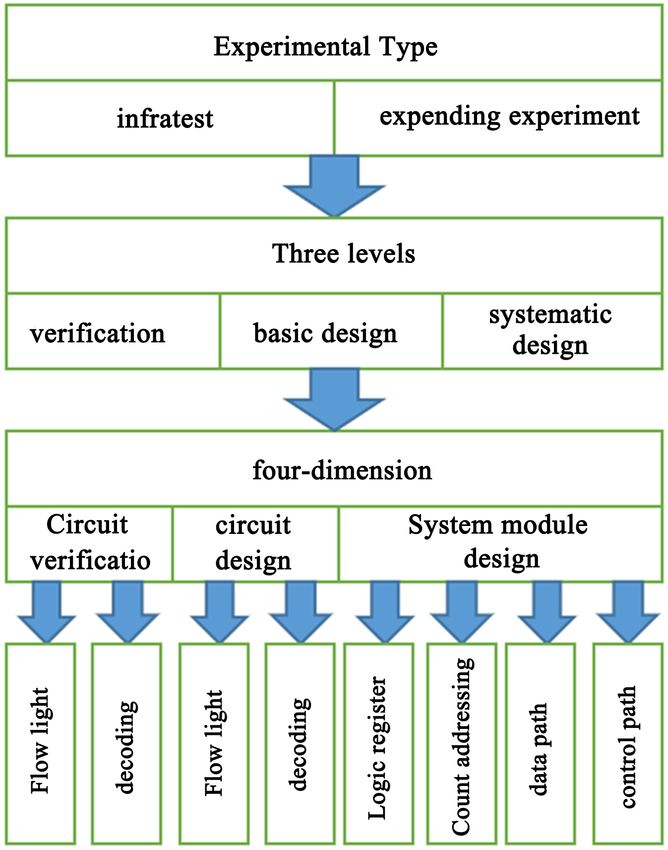
L. Zhao

                               devices has also changed from simple combination to complex logic [3]. Realiza-
                               tion becomes a complex high-speed digital logic control, various high-speed al-
                               gorithm realizations and special-purpose microprocessors for constructing spe-
                               cial functions, etc. High-density, complex logic and extremely high operating
                               frequency have caused profound and revolutionary changes in design methods,
                               design tools, and verification of current digital logic [4] [5] [6].
                                  Digital circuit experiment is based on “Digital Circuit and Logic Design”,
                               which is the basic core course of electronic majors [7] [8]. This professional
                               course requires students to be able to master the analysis and design of digital
                               logic circuits and to use them further. The requirements for practice are rela-
                               tively high [9]. Therefore, in the whole teaching task, after students master the
                               basic circuit knowledge, digital circuit experiment shoulders the task of cultivat-
                               ing professional application ability, so it has an indispensable position in the
                               overall teaching [10] [11].
                                  In recent years, based on the development of modern digital electronic tech-
                               nology and the educational concept of advancing with the times, the experimen-
                               tal teaching of digital circuits has innovated the experimental platform, experi-
                               mental content and experimental form [12]. First of all, the traditional experi-
                               mental method is to build a digital circuit by 74 series gate circuits [13]. Because
                               this method is too far from the realization of the digital circuit industry, our dig-
                               ital circuit experiment platform has transitioned to use CPLD, FPGA and other
                               programmable logic devices [14] [15]. The new platform uses a combination of
                               software and hardware, which can be easily built on any computer, and the ex-
                               perimental equipment is small and portable. Secondly, the experimental content
                               has changed from verification to comprehensive and innovative design experi-
                               ments, from a single, independent basic circuit realization to a complex system
                               circuit design [16]. As the number of experimental steps increases, possible
                               problems become more complicated [17]. Finally, there are certain changes in
                               the experimental format. Through pre-class preview, program design, sub-module
                               implementation, system integration and other links, the classroom efficiency has
                               been improved, and students’ thinking and practical skills have been enhanced
                               [18] [19]. The experimental form has changed from a pure classroom experi-
                               ment to a form of extracurricular debugging combined with in-class centralized
                               problem solving [20]. These improvement methods aim to promote teaching
                               and learning, making the course of digital circuit conform to the teaching con-
                               cept of CDIO, and cultivate talents of electronic technology under the back-
                               ground of new engineering education.

                               2. Experimental Ideas
                               Since the establishment of the digital circuit experiment, some confirmatory ex-
                               periments on 74 series chips have been the main focus. With the changes in the
                               use, carrier, and design verification methods of modern digital logic circuits,
                               many colleges and universities have reformed digital circuit experiments in
                               terms of experimental content design, device use, design methods and verifica-

DOI: 10.4236/wjet.2021.92024                        347                  World Journal of Engineering and Technology
L. Zhao
tion methods. After investigation, they found that they can be summarized as
follows:
1) Replace the main experimental devices, and replace the original 74 series
gate circuits with programmable logic devices such as CPLD and FPGA.
2) Change the experimental form, abandon the experimental form of manual-
ly connecting the circuit on the breadboard or experiment box, and replace it
with EDA tools to design and debug the circuit.
3) Expand experimental content and introduce comprehensive and innovative
design experimental content.
Traditional experimental teaching is based on 74 series chips, which are used
to build circuits on the experiment box for experimental research. This method
allows students to perform manual wiring, which is more cumbersome, high in
time and costly, and out of touch with the industry. After changes, the current
digital circuit experiments are basically in line with the current mainstream
technology in terms of experimental devices, digital circuit design and verifica-
tion, and use EDA simulation software for teaching [21]. But this is not to say
that there are no problems. In this teaching method, students in the lower grades
must not only learn the knowledge of circuits, but also learn the operation of the
software. EDA software is powerful, but it is more difficult for students in lower
grades to learn, which affects their interest in learning. The digital and electrical
experiment belongs to the basic experiment in the electronic professional teach-
ing and training system. Its task is to support theoretical teaching first. There are
a lot of content in theoretical teaching about various simple gate circuits and
triggers. For this part of the content, how to simple, Intuitive experimental
demonstration and verification of them, so as to impress the students, this is a
big problem. Some students emphasize circuit design and software simulation,
and even think that digital circuit design is equivalent to software simulation,
ignoring the importance of verification with experiment boards, and a deviation
in the overall understanding of digital circuits. Finally, the connection between
comprehensive and innovative design experiment content and basic experiment,
proportional distribution, difficulty control and other issues need to be further
studied [22].
3. Digital Circuit Experiment Design Based on FPGA
Aiming at the problem of students ignoring the experiment board, FPGA is used
as the experimental hardware platform. Students are required to download the
designed circuit to the board every time they experiment, debug and verify the
circuit on the experiment board, and train students to use instruments, software
and hardware to learn the capabilities of digital circuits. The difficulty of the ex-
periment is progressive, divided into three levels: basic, expansion and synthesis,
to solve the problem of connection between different types of experiments, and
finally achieve the goal of designing a complex digital system. Through the
teacher’s explanation and the students’ personal operation, the students will
gradually become familiar with the EDA software [23]. The initial experiments
DOI: 10.4236/wjet.2021.92024 348 World Journal of Engineering and TechnologyL. Zhao
are relatively simple and basic, with more verifying content and less design con-
tent. Simple and intuitive experiments are mainly used to verify the knowledge
points of theoretical teaching. Through this part of the experiment, students will
become familiar with the operation of the software as soon as possible and pre-
pare for subsequent experiments. This allows students to focus more on circuit
design in the design experiment, reducing the problems caused by unskilled op-
erations. Subsequent experiments introduced complex content step by step. Try
to minimize the impact of platform and design difficulty changes on students, so
that they can gradually master digital circuit development skills.
3.1. Experimental Platform Reform
The designed FPGA experimental platform has relatively complete functions,
especially in terms of lower board verification and hardware debugging, which
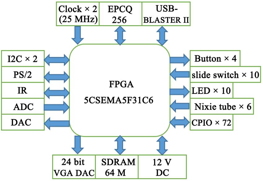
shows good operability and flexibility. Figure 1 is a simplified block diagram of
the experimental hardware platform module. According to the experimental ap-
plication, it can be summarized as: programmable logic device, FPGA uses
ALERA’s CYCLONE V series, containing 85 K programmable logic device, 4450
Kb embedded memory unit; on-board resources, Peripherals are equipped with
buttons, LEDs, digital tubes and other devices for off-board verification. 72
GPIOs are reserved on the board as expansion ports for supply expansion, func-
tion customization and debugging; supporting components, providing external
clocks, USB-Blaster debuggers, etc. for experiments support.
The Quartus II 13.1 used in the development environment includes solutions
for all stages of the FPGA development process. It has the advantages of short
design cycle, easy operation, strong design flexibility, and rich debugging me-
thods. Based on the above platform, the circuit design and verification methods
are changed, so that students are well trained in both soft and hard aspects. Stu-
dents first complete design input and synthesis on Quartus II. The specific
adaptation chip and placement and routing are automatically completed by the
computer, replacing the traditional manual routing experiment. Then use
Quartus II to call ModelSim-Altera 10.1d co-simulation and debugging, and test
Figure 1. The diagram of FPGA experimental system.
DOI: 10.4236/wjet.2021.92024 349 World Journal of Engineering and TechnologyL. Zhao
the circuit function preliminarily without the aid of instruments. When verifying
on the board, download the generated .sof file to the actual operation of the
FPGA observation circuit. The experiment effect can be designed according to
the onboard resources of the experiment platform, which adds to the fun of the
experiment. For comprehensive debugging, the experimental platform reserves
debugging ports and FPGA resources to support various signal observation me-
thods such as instrument testing and online logic analyzer monitoring.
The new platform eliminates the need for manual wiring on the experimental
box, greatly reducing unnecessary labor time and allowing students to focus on
circuit design while significantly improving efficiency. For example, the overall
experiment time was reduced by 20% for the LED flow-light experiment after
the new platform was adopted. For the traffic light design, the experiment time
was reduced by 15%.
3.2. Experimental Planning and Content Reform
The selection of experiment content not only considers the theoretical and holis-
tic nature of the course itself, but also considers the systematic nature of the ex-
periment and subsequent professional courses. The experimental system struc-
ture is shown in Figure 2. The experiment covers three stages to master a new
technology, and a complete experimental system is formed by several experi-
mental items with increasing difficulty. The preliminary experiment is the basis
of the subsequent experiment, and the subsequent experiment is the application
of the preliminary experiment.
The introductory experiment is for beginners to familiarize themselves with
the new experimental platform and to intuitively verify the theoretical teaching
Figure 2. Schematic diagram of digital circuit experimental structure.
DOI: 10.4236/wjet.2021.92024 350 World Journal of Engineering and TechnologyL. Zhao
knowledge points based on the platform. This experiment calls the common de-
vice library that comes with quartus, and uses the method of schematic drawing
to simulate traditional experiments to verify various simple gate circuits,
flip-flops and module circuits on a breadboard or experiment box. The experi-
ment requires students to verify the functions of the 74LS138 and the 4-input
16-output decoder composed of 2 pieces of 74LS138 through the lower board
and the instrument on the FPGA platform. The operation involved in the whole
process is very basic, which can avoid the problem of poor reliability and flex-
ibility of manual wiring.
The basic design part self-modeling to realize the 74LS138 in the verification
circuit is used to compare and analyze the difference between the standardized
module circuit and the self-modeling design circuit. The transition from the tra-
ditional experimental form to the self-designed circuit using verilog HDL. Each
experimental project at this stage requires a complete experimental process cov-
ering hardware modeling, software simulation, board verification, and compre-
hensive debugging. In the basic circuit design, the concept of timing is added to
the water lamp circuit, and the circuit complexity is improved compared with
the decoder. The advanced part of the basic design designs and verifies the sim-
plified instruction set CPU functional components, such as addressing units,
arithmetic logic units, etc., obtained from the combination of basic circuits or
expanded functions. The circuit structure designed in the early stage of the expe-
riment is simple, and students can devote more energy to the study of EDA
software. With the gradual increase in modeling complexity, the software opera-
tion becomes more and more proficient, and more attention can be paid to the
learning of logic description language and the improvement of circuit analysis
and debugging capabilities in the later period.
The expansion experiment begins with the practical sequence of module cir-
cuit, subsystem circuit to system circuit design, and gradually integrates the ba-
sic circuit into components, and then the components work together to form a
simplified CPU system. According to the pre-set instruction set architecture, bus
structure, circuit structure and other index parameters, the students design the
number of instructions to be 24. The address, data bus, and I/O interface are all
16-bit simplified instruction set CPUs. The lower board verification link requires
the CPU to automatically read the instructions in the memory and operate the
I/O interface level to realize the running light. Students design circuits to im-
plement CPU functions such as data access, data processing, and interface con-
trol, which will help students to deeply understand the supporting role of digital
logic circuits for subsequent courses such as microcomputer principles, com-
puter composition principles, and ASIC design.
4. Module Realization of the Experimental System
4.1. Key Module
In order for the system to accurately identify the operation of the buttons, it is
DOI: 10.4236/wjet.2021.92024 351 World Journal of Engineering and TechnologyL. Zhao
necessary to perform debounce and release detection processing on the keys.
Key debounce can be divided into hardware debounce and software debounce.
In order to simplify the experimental process, this article uses software debounce
to obtain stability. The theoretical button jitter time is 5 - 10 ms. For this, the
button module first defines a timer with a duration of 15 ms, and then judges the
level signal of the corresponding port after the button is pressed for 15 ms.
The realization method of letting go detection is shown in Formula (1):
key_press = key_reg & (~key_reg_next), (1)
In the Formula (1), key_press is a register variable indicating whether the key
press is valid, key_reg stores the state of the key at the current moment, and
key_reg_next is the state of the key at the next moment. From Formula (1), it
can be seen that if key_press is 1, key_reg must be 1 and key_reg_next It must be
0, and its corresponding meaning is: only the key is not pressed at the current
moment, and is pressed at the next moment, it is recognized as a valid key trig-
ger signal. Figure 3 is the gate-level circuit diagram of the release detection me-
thod.
4.2. Timing Module
The timing module first defines a timer with a duration of 1s as the counter
clock reference. The design idea of this module is to use the 1s timer to complete
the counting of unit seconds, and then according to the unit second and unit
minute and unit minute and unit hour. Figure 3 is a block diagram of the reali-
zation of the unit second. The second digit is composed of the second digit and
the second tens digit, and the value is cyclically changed between 0 and 59. The
realization process of the unit second is the modulo sixty counter. Implementa-
tion process. The module first defines the modulus ten counter to complete the
counting of the second digit, and then defines the modulus six counter, and cas-
cades the modulus ten counter and the modulus six counter in a serial carry way
to complete the realization of the modulus sixty counter. Each one After the 60s
count is completed, the units digit and tens digit of the second are cleared, and
the carry output bit of the tens digit of the second is carried to the units digit of
the unit minute to complete the clock halving.
4.3. Digital Tube Module
The six eight-segment digital tubes of the experimental platform are connected
Figure 3. Gate level circuit diagram of detection function realization.
DOI: 10.4236/wjet.2021.92024 352 World Journal of Engineering and TechnologyL. Zhao
to the SEG_EN0 - SEG_EN5 pins in the FPGA as the chip selection terminal of
the FPGA using a common cathode method. The a - g and decimal point dp pins
of the 6 digital tubes are connected in parallel to the FPGA’s SEG_DATAa -
SEG_DATADP pins are used as data input terminals. The experiment uses dy-
namic scanning to allow 6 digital tubes to display the current hour, minute, and
second information at the same time. The module defines a 1ms timer as the
scanning period of the dynamic scanning digital tube. In the period of time, the
time information to be displayed is decoded first. According to the actual situa-
tion, only the 10 numbers 0 - 9 are decoded. After the decoding is completed, the
decoded result is assigned to SEG_DATAx (x = a, b... DP). At the same time,
pull down the corresponding digital tube chip selection end, and the corres-
ponding time information will be displayed on the digital tube. The next time
information will be scanned and displayed every 1ms. Visual persistence, when
you see the hour, minute, and second information, it will be displayed on the
digital tube at the same time.
4.4. Top-Level Module
After using the hardware description language (Verilog HDL) to describe the
functions to be implemented by each module, write the top-level module to
connect the sub-modules. Use the analysis and synthesis tools of Quartus II to
compile the project and generate the RTL (Register Transfer Level) function. It
can be seen from the figure that the digital clock system is divided into 4 mod-
ules, and the internal ports and external ports of the system are consistent with
the system to be designed.
4.5. Hardware Verification
After using Model to perform software simulation on each module and the en-
tire circuit, ensure that the functions of each module are normal, and finally
download the compiled “sof” file to the FPGA development board through the
download line. First, complete the clock hour, minute and second setting by
pressing the button. Then press the start button to start timing. When the clock
reaches the hour, the buzzer can beep for 1s. After actual inspection, the de-
signed digital clock can operate normally and meet the expected design re-
quirements.
5. Summary and Conclusions
This article takes the current problems of digital circuit experiments as a starting
point, and proposes practical reform measures from both the experimental plat-
form and experimental content. The reformed digital circuit basic experiment
can not only simultaneously support the “digital logic circuit and system” theo-
retical course, but also provide a complete set of modern digital integrated cir-
cuit development tutorials. Through experimental design from easy to difficult,
students construct a correct understanding of modern digital circuit design in
DOI: 10.4236/wjet.2021.92024 353 World Journal of Engineering and TechnologyL. Zhao
experimental teaching, train digital circuit design, analysis, verification and de-
bugging capabilities, and effectively cultivate students’ comprehensive quality of
engineering practice. Since the circuit design method and verification method of
each experimental project are basically the same, the difficulty of the experiment
is reflected in the difference in modeling complexity. This difference depends on
the level of the CPU. The pre-order experiment is the basis of the post-order ex-
periment, and the post-order experiment is the application of the pre-order ex-
periment. The students’ logic description language application ability and circuit
analysis and debugging ability gradually increase as the difficulty of the experi-
ment increases. Get trained.
The experimental reform has been applied for two years, and has been conti-
nuously adjusted through teaching practice and student feedback, and has
achieved remarkable results. Practice has proved that the experiment can not
only help students better learn and understand theoretical knowledge, but also
enable them to master the method of designing and implementing digital sys-
tems based on FPGA. According to the questionnaire survey, 90% of the stu-
dents think that the experiments conducted on the new platform can stimulate
their enthusiasm for learning and have the desire for further research. This per-
centage is higher than the results of the questionnaire when using the old plat-
form. In the return visit, most students said that the experiment was very helpful
to their understanding of the basic concepts and principles in the “Digital cir-
cuit” course.
Acknowledgements
This work was funded by Collaboration between industry and school Project of
Ministry of Education: “Innovative teaching and training of PAEE system in
electronic information major” (No. 201901103032).
Conflicts of Interest
The author declares no conflicts of interest regarding the publication of this pa-
per.
References
[1] Carroll, L., Lee, J.S., Scarcella, C., et al. (2016) Photonic Packaging: Transforming
Silicon Photonic Integrated Circuits into Photonic Devices. Applied Sciences, 6, 426.
https://doi.org/10.3390/app6120426
[2] Grout, I.A. (2005) Integrated Circuit Test Engineering: Modern Techniques. Sprin-
ger Science & Business Media, Berlin.
[3] Ayers, J.E. (2018) Digital Integrated Circuits: Analysis and Design. CRC Press, Boca
Raton. https://doi.org/10.1201/b12491
[4] Kocur, M., Kozak, S. and Dvorscak, B. (2014) Design and Implementation of FPGA-
Digital Based PID Controller. Proceedings of the 2014 15th International Carpa-
thian Control Conference (ICCC), Velke Karlovice, 28-30 May 2014, 233-236.
https://doi.org/10.1109/CarpathianCC.2014.6843603
DOI: 10.4236/wjet.2021.92024 354 World Journal of Engineering and TechnologyL. Zhao
[5] Sankarayya, N., Roy, K. and Bhattacharya, D. (1997) Algorithms for Low Power and
High Speed FIR Filter Realization Using Differential Coefficients. IEEE Transac-
tions on Circuits and Systems II: Analog and Digital Signal Processing, 44, 488-497.
https://doi.org/10.1109/82.592582
[6] Noll, T.G. (1991) Carry-Save Architectures for High-Speed Digital Signal Processing.
Journal of VLSI Signal Processing Systems for Signal, Image and Video Technology,
3, 121-140. https://doi.org/10.1007/BF00927839
[7] Martin, K.W. (2000) Digital Integrated Circuit Design. Oxford University Press,
New York.
[8] Holdsworth, B. and Woods, C. (2002) Digital Logic Design. Elsevier, Amsterdam.
[9] Zemva, A., Trost, A. and Zajc, B. (1998) A Rapid Prototyping Environment for Teaching
Digital Logic Design. IEEE Transactions on Education, 41, 342.
https://doi.org/10.1109/13.728275
[10] Obaid, Z.A., Sulaiman, N. and Hamidon, M.N. (2009) FPGA-Based Implementation
of Digital Logic Design Using Altera DE2 Board. International Journal of Computer
Science and Network Security, 9, 186-194.
[11] Farooq, U., Marrakchi, Z. and Mehrez, H. (2012) FPGA Architectures: An Overview.
In: Tree-Based Heterogeneous FPGA Architectures, Springer, New York, 7-48.
https://doi.org/10.1007/978-1-4614-3594-5_2
[12] Sulaiman, N., Obaid, Z.A., Marhaban, M.H., et al. (2009) FPGA-Based Fuzzy Logic:
Design and Applications—A Review. International Journal of Engineering and Tech-
nology, 1, 491. https://doi.org/10.7763/IJET.2009.V1.90
[13] Lala, P.K. and Burress, A.L. (2003) Self-Checking Logic Design for FPGA Imple-
mentation. IEEE Transactions on Instrumentation and Measurement, 52, 1391-
1398. https://doi.org/10.1109/TIM.2003.818545
[14] Shi, J. and Deng, C. (2010) Digital Circuit Experiment System Based on FPGA. 2010
International Conference on E-Health Networking Digital Ecosystems and Tech-
nologies (EDT), Vol. 2, 277-280. https://doi.org/10.1109/EDT.2010.5496371
[15] Brown, S. and Rose, J. (1996) Architecture of FPGAs and CPLDs: A Tutorial. IEEE
Design and Test of Computers, 13, 42-57. https://doi.org/10.1109/54.500200
[16] Tzou, Y.Y. and Hsu, H.J. (1997) FPGA Realization of Space-Vector PWM Control
IC for Three-Phase PWM Inverters. IEEE Transactions on Power Electronics, 12,
953-963. https://doi.org/10.1109/63.641493
[17] Tuna, M. and Fidan, C.B. (2016) Electronic Circuit Design, Implementation and
FPGA-Based Realization of a New 3D Chaotic System with Single Equilibrium Point.
Optik, 127, 11786-11799. https://doi.org/10.1016/j.ijleo.2016.09.087
[18] Jung, S.L., Chang, M.Y., Jyang, J.Y., et al. (1999) Design and Implementation of an
FPGA-Based Control IC for AC-Voltage Regulation. IEEE Transactions on Power
Electronics, 14, 522-532. https://doi.org/10.1109/63.761696
[19] Vaidyanathan, S., Pehlivan, I., Dolvis, L.G., et al. (2020) A Novel ANN-Based
Four-Dimensional Two-Disk Hyperchaotic Dynamical System, Bifurcation Analy-
sis, Circuit Realisation and FPGA-Based TRNG Implementation. International Jour-
nal of Computer Applications in Technology, 62, 20-35.
https://doi.org/10.1504/IJCAT.2020.103921
[20] Sambas, A., Vaidyanathan, S., Tlelo-Cuautle, E., et al. (2019) A Novel Chaotic Sys-
tem with Two Circles of Equilibrium Points: Multistability, Electronic Circuit and
FPGA Realization. Electronics, 8, 1211. https://doi.org/10.3390/electronics8111211
[21] Qin, L., Wang, X. and Guan, J. (2009) Application of EDA Simulation in Designing
Experiments of Computer Organization. Research and Exploration in Laboratory,
DOI: 10.4236/wjet.2021.92024 355 World Journal of Engineering and TechnologyL. Zhao
28, 79-82.
[22] Tian, J. and Xia, L. (2005) Teaching Practice of EDA-Based Electronic Technology.
Theory and Practice of Education, 12, 22.
[23] Jie, D. (2012) Simulation Software Applied in Electronic Technology Teaching. 2012
IEEE International Conference on Industrial Control and Electronics Engineering,
Xi’an, 23-25 August 2012, 925-927. https://doi.org/10.1109/ICICEE.2012.245
DOI: 10.4236/wjet.2021.92024 356 World Journal of Engineering and TechnologyYou can also read