High detection efficiency silicon single-photon detector with a monolithic integrated circuit of active quenching and active reset
←
→
Page content transcription
If your browser does not render page correctly, please read the page content below
High detection efficiency silicon single-photon detector with a monolithic
                                                   integrated circuit of active quenching and active reset
                                                             Yu-Qiang Fang,1, 2 Kai Luo,3, 4 Xing-Guo Gao,3 Gai-Qing Huo,3 Ang Zhong,3 Peng-Fei Liao,3 Pu Pu,3 Xiao-Hui
                                                             Bao,1, 2 Yu-Ao Chen,1, 2 Jun Zhang,1, 2, a) and Jian-Wei Pan1, 2
                                                             1)
                                                                Hefei National Laboratory for Physical Sciences at the Microscale and Department of Modern Physics,
                                                             University of Science and Technology of China, Hefei 230026, China
                                                             2)
                                                                CAS Center for Excellence in Quantum Information and Quantum Physics,
                                                             University of Science and Technology of China, Hefei 230026, China
                                                             3)
                                                                Sichuan Institute of Solid-State Circuits, China Electronics Technology Group Corp., Chongqing 400060,
                                                             China
                                                             4)
                                                                College of Optoelectronic Engineering, Chongqing University, Chongqing 400044,
                                                             China
arXiv:2011.09595v1 [physics.ins-det] 19 Nov 2020

                                                             (Dated: 20 November 2020)
                                                             Silicon single-photon detectors (SPDs) are key devices for detecting single photons in the visible wavelength
                                                             range. Photon detection efficiency (PDE) is one of the most important parameters of silicon SPDs, and
                                                             increasing PDE is highly required for many applications. Here, we present a practical approach to increase
                                                             PDE of silicon SPD with a monolithic integrated circuit of active quenching and active reset (AQAR). The
                                                             AQAR integrated circuit is specifically designed for thick silicon single-photon avalanche diode (SPAD) with
                                                             high breakdown voltage (250-450 V), and then fabricated via the process of high-voltage 0.35-µm bipolar-
                                                             CMOS-DMOS. The AQAR integrated circuit implements the maximum transition voltage of ∼ 68 V with
                                                             30 ns quenching time and 10 ns reset time, which can easily boost PDE to the upper limit by regulating the
                                                             excess bias up to a high enough level. By using the AQAR integrated circuit, we design and characterize two
                                                             SPDs with the SPADs disassembled from commercial products of single-photon counting modules (SPCMs).
                                                             Compared with the original SPCMs, the PDE values are increased from 68.3% to 73.7% and 69.5% to 75.1%
                                                             at 785 nm, respectively, with moderate increases of dark count rate and afterpulse probability. Our approach
                                                             can effectively improve the performance of the practical applications requiring silicon SPDs.

                                                   I.   INTRODUCTION                                                depletion layer of tens of micrometers, high Vbr (250-
                                                                                                                    450 V), and large active area. SPCM exhibits ∼ 70%
                                                      Single-photon detectors (SPDs) are the most sensi-            PDE at 650 nm, 25 cps DCR (best grade), and ∼ 400 ps
                                                   tive tools to detect extremely weak light and are widely         Tjitter . The third one is the SPAD device fabricated via
                                                   used in numerous applications1 . Currently, there are            the complementary metal–oxide–semiconductor (CMOS)
                                                   several SPD technologies such as photomultiplier tubes           technology, which exhibits ∼ 45% PDE at 450 nm10 . The
                                                   (PMTs), superconducting nanowire single-photon detec-            quenching circuit is crucial for SPAD to achieve high
                                                   tors2,3 , and single-photon avalanche diodes (SPADs)4,5 ,        performance, in which SPAD is operated either in gat-
                                                   among which using SPADs is the primary solution for              ing mode or in free-running mode. So far, high detec-
                                                   practical applications due to the advantages of small size       tion efficiency silicon SPDs using high-frequency gating
                                                   and low cost. In the visible wavelength range, silicon           techniques have been reported11–13 . For the free-running
                                                   SPADs are normally used to detect single photons6 . The          mode, passive quenching is a simple solution4,7,14,15 , how-
                                                   key parameters for characterization include photon de-           ever, it suffers from low CRmax and slow recovery. Active
                                                   tection efficiency (PDE), dark count rate (DCR), after-          quenching overcomes the drawbacks of passive quench-
                                                   pulse probability (Pap ), maximum count rate (CRmax ),           ing while brings the challenges to the electronics design
                                                   and timing jitter (Tjitter ).                                    in terms of short quenching time and reset time. So far,
                                                      A silicon SPD is composed of a SPAD and the corre-            various approaches to active quenching circuits have been
                                                   sponding quenching circuit7 . There are three kinds of sil-      reported16–26 . For instance, the circuits of SPCMs adopt
                                                   icon SPADs4 . The first one is the thin silicon SPAD, e.g.,      an approach of double quenching, i.e., passive quenching
                                                   PDM photon counting module8 , which is a planar epitax-          at the cathode and active quenching at the anode27 . The
                                                   ial device with thin depletion layer of a few micrometers,       circuits use discrete devices and the excess bias voltage is
                                                   low breakdown voltage (Vbr ) (15-40 V), and small ac-            limited due to the breakdown voltage of the transistors.
                                                   tive area. Such SPAD exhibits ∼ 50% PDE at 550 nm,                  In this paper, we present an approach to increase
                                                   ∼ 50 cps DCR, and ∼ 50 ps Tjitter . The second one is            PDE of silicon SPD to the upper limit with a mono-
                                                   the thick silicon SPAD, e.g., single-photon counting mod-        lithic integrated circuit of active quenching and active
                                                   ule (SPCM)9 , which is a reach-through device with thick         reset (AQAR). The AQAR integrated circuit is specifi-
                                                                                                                    cally designed for the thick silicon SPAD and is fabricated
                                                                                                                    via the process of high-voltage 0.35-µm bipolar-CMOS-
                                                                                                                    DMOS (BCD), with the maximum transition voltage of
                                                   a) Electronic   mail: zhangjun@ustc.edu.cn                       ∼ 68 V, 30 ns quenching time, and 10 ns reset time.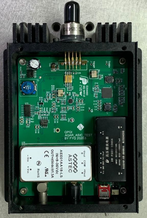
2

                                                  Vdd               Vcc                        Vhigh

                                                                   D1
                                                              R1
                                                                           R2              SPAD
                                                     M1            C1       D2
                                                                                              IN

                        QUENCHING
                                                                                  R3         OUT_1
                                                      M2
                             RESET
                                                                                  R4         OUT
                             GND                                   M3        M4

                                     FIG. 1. Schematic diagram of the AQAR circuit.

We also develop two silicon SPDs using the AQAR chips              Since the QUENCHING signal is at the logic level LOW,
and SPADs disassembled from commercial products of                 M2 turns off and M1 turns on. The bootstrap capacitor
SPCMs. The characterization results show that com-                 C1 maintains M1 in the linear region of operation so that
pared with the original SPCMs, the PDE values of SPDs              the voltage at the IN node keeps growing to Vdd . In such
can be increased from 68.3% to 73.7% and 69.5% to                  a way, the voltage difference between the cathode and an-
75.1% at 785 nm, respectively, with moderate increases             ode of the silicon SPAD is changed to Vhigh − Vdd , which
of DCR and Pap .                                                   is below Vbr . Therefore, the avalanche process is com-
                                                                   pletely quenched. After a controlled hold-off time, the
                                                                   signal at the RESET pin is set at the logic level HIGH,
                                                                   which results in that M3 and M4 turn on promptly to re-
II. INTEGRATED CIRCUIT DESIGN AND
                                                                   set the voltage at the IN node to zero. Then, the AQAR
FABRICATION
                                                                   circuit is recovered to the initial quiescent state for the
                                                                   next single-photon detection.
   Fig. 1 illustrates the schematic diagram of the AQAR
integrated circuit. The anode of the silicon SPAD is con-             The AQAR chip is fabricated via the process of high-
nected to the IN pin of the chip. In order to achieve              voltage 0.35-µm BCD. The BCD process combines the
fast voltage transition, four n-channel DMOS transistors           advantages of three different processing technologies into
(M1-M4) are designed, among which M1 and M2 are used               a single chip, among which DMOS is specifically suited
for quenching switches while M3 and M4 are used for re-            for high-voltage circuits. During the process, the triple
set switches. The input signals from the QUENCHING                 well process with a deep n-well is used to fabricate the
pin and the RESET pin are in the transistor-transistor             isolated thick gate oxide NLDMOS (N-channel Later-
logic (TTL) level. They are converted into signals with            ally Diffused Metal Oxide Semiconductor) transistors
12 V amplitude (Vcc ) to improve the drive capability by           and high-voltage diodes. The drain-to-source, source-
two drivers that are integrated into the AQAR circuit, as          to-substrate, and drain-to-substrate breakdown voltages
shown in the inset of Fig. 1.                                      of the transistors are ∼ 100 V. The reverse breakdown
   In a quiescent condition, the quenching signal is at the        voltages of the diodes are ∼ 80 V. The resistors are im-
logic level HIGH to make M2 on while the reset signal is           plemented by injecting two layers of polysilicon among
at the logic level LOW to make M3 and M4 off. Since M2             four layers of metal wiring, and the resistance values are
turns on, the gate voltage of M1 is below the threshold            regulated by the doping concentration of polysilicon. A
and thus M1 turns off. The voltage at the IN node is close         metal capacitor filled with a nitride medium is also inte-
to zero. The bias voltage (Vhigh ) is above Vbr . The SPAD         grated. The breakdown voltage between the plates of the
is ready for single-photon detection, and the whole circuit        capacitor is 14 V, and the breakdown voltages between
is in the quiescent state. Once an avalanche occurs, the           the plates and the substrate are ∼ 100 V. The AQAR
avalanche current immediately produces a voltage drop              chip is then sealed inside a ceramic small outline package
on the resistors of R3 and R4. R3 is a relatively high-            with an overall dimension of 11 mm × 5 mm, as shown
value resistor to quench the avalanche passively and R4            in Fig. 2a. Fig. 2b shows the microphotograph of the die
is used as a voltage divider to produce an output signal           inside the AQAR chip with a dimension of 1.1 mm × 1.1
for discrimination. The inverse output signal from the             mm. The dimension of the pad for bonding is 130 µm ×
discriminator is connected with the QUENCHING pin.                 130 µm.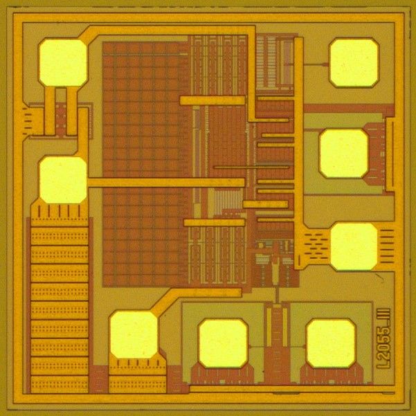
3
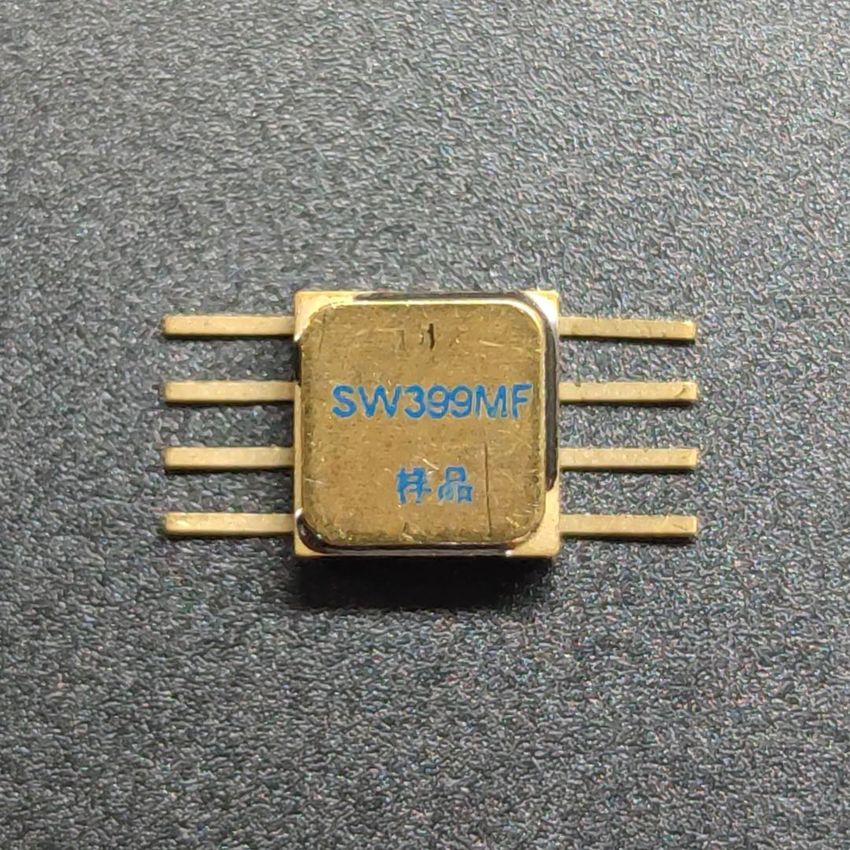
(a) (b) Vdd IN
Vcc
5 mm
RESET
11 mm
QUENCHING GND OUT OUT_1
FIG. 2. (a) Photo of the AQAR chip with an overall package dimension of 11 mm × 5 mm. (b) Microphotograph of the die
inside the AQAR chip.
III. SPD MODULE AND CHARACTERIZATION ps pass through a variable optical attenuator (VOA),
a 99:1 beam splitter (BS), and a fixed optical attenu-
Further, we design an SPD module with the AQAR ator (FOA). Then, the intensity of the laser pulses is
chip. Fig. 3a illustrates the schematic diagram of the attenuated down to a level of a mean photon number per
SPD module, the corresponding single-photon calibration pulse of 1. The 99% port of the BS is monitored with a
system, and the measurement setup. Fig. 3b exhibits the power meter (PM, Newport). A time-to-digital converter
photo of the designed SPD module, with a dimension of (TDC, PicoQuant) is used to perform measurements and
128 mm × 103 mm × 33 mm, a weight of 380 g, and a transmit data to a personal computer (PC), so that the
power dissipation of ∼ 3.5 W. In the module, the silicon parameters of PDE, DCR, Pap , CRmax , and Tjitter can
SPAD is biased with a tunable high-voltage power sup- be calculated.
ply (Vhigh ). The temperature of the SPAD is regulated
by a thermoelectric cooler (TEC) controller. The anode
of the SPAD is connected as close as possible to the IN IV. RESULTS AND DISCUSSION
pin of the AQAR chip. The avalanche signal from the
OUT pin is discriminated by a high-speed comparator, We perform single-photon characterization of SPDs at
and the subsequent monostable circuit produces a 20 ns 785 nm with two silicon SPADs disassembled from com-
LOW-level effective signal connected with the QUENCH- mercial products of SPCMs (part numbers: SPCM-800-
ING pin. The propagation delay between the OUT pin 24-FC 38234 and SPCM-800-24-FC 38470) and compare
and the QUENCHING pin is calibrated to be as low as 3 the parameters between our SPDs (part numbers: AQAR
ns. Also, the monostable circuit produces a 10 ns HIGH- 38234 and AQAR 38470) and the original SPCMs. The
level effective signal connected with the RESET pin after operating temperatures of SPADs in our SPDs are reg-
a certain hold-off time. The hold-off time can be tuned ulated as that in SPCMs, i.e., 252 K, by measuring the
from 0 to 180 ns by delay lines, which is used to re- resistance of the thermistor in the SPADs. For our SPDs,
duce the afterpulse probability. Fig. 3c plots a typical the hold-off time is set to 40 ns and the overall dead time
voltage waveform captured by an oscilloscope at the IN is ∼ 82 ns. Fig. 4 shows the measured results in two
pin, from which one can observe that the overall dead cases. For SPCMs, Vbr of two SPADs is calibrated to be
time of SPD is contributed by four processes, i.e., pas- 339.5 V and 355.0 V at 252 K, and PDE is measured to
sive quenching, active quenching, hold-off duration, and be 68.3% and 69.5%, respectively, with ∼ 30 V Vex .
active reset. By setting Vdd to the maximum value, i.e., Fig. 4a and Fig. 4b plot PDE as a function of excess
∼ 68 V, the quenching time and the reset time are mea- bias. With the increase of excess bias, PDE continues
sured to be 30 ns and 10 ns, respectively. Moreover, by to increase. When Vex reaches ∼ 55 V, PDE becomes
setting the hold-off time to the minimum value, the volt- flat, which implies that PDE is very close to the upper
age waveform persistence, as shown in Fig. 3d, indicates limit. The parameters of DCR and Pap as a function
that the intrinsic dead time of SPD is ∼ 42 ns. of PDE for two SPDs are also plotted in Fig. 4c and
Following the single-photon calibration scheme5 , one Fig. 4d, respectively, from which one can clearly observe
channel (CH1) of the signal generator (SG) generates that the PDE of our SPDs is significantly higher than
a clock of 100 kHz to drive a picosecond pulsed laser SPCMs with a cost of moderate increases of DCR and
diode (LD, PicoQuant) at 785 nm. The laser pulses Pap . The detailed results for the comparison are listed in
with a full width at half maximum (FWHM) below 70 Table I. Compared with the original SPCMs, the PDE4
(a)
(c)
SPD module Vhigh Calibration system
PM
BS
Vdd Vcc TEC VOA LD
SPAD FOA
Vdd Vcc
RESET IN
QUENCHING OUT_1 PC SG
GND AQAR OUT TDC Ch1
Stop Start SYNC
Measurement setup
DELAY PCB Trace
Coaxial cable
Optical fiber
(b)
TEC controller (d)
Vhigh
SPAD
103 mm
AQAR chip
128 mm
FIG. 3. (a) Schematic diagram of the SPD module and the experimental setup for single-photon characterization at 785 nm.
(b) The photo of the SPD module. (c) A typical voltage waveform captured by an oscilloscope at the anode of the silicon
SPAD. (d) The voltage waveform persistence at the anode of the silicon SPAD with Vdd = 68 V and the minimal hold-off time
shows that the intrinsic dead time is ∼ 42 ns.
TABLE I. Parameter comparison between SPCMs and SPDs with the AQAR integrated circuits for the same SPADs at 785
nm. ∆P DE represents the relative increase value of PDE.
Part number PDE DCR (cps) Pap Tjitter (ps) CRmax (MHz) ∆P DE
SPCM 800 24 FC 38234 0.683 48.5 0.021 430 31.0
0.08
AQAR 38234 0.737 96.4 0.057 370 10.1
SPCM 800 24 FC 38470 0.695 54.4 0.023 460 31.0
0.08
AQAR 38470 0.751 99.7 0.062 390 10.2
values of our SPDs are increased from 68.3% to 73.7% ing high detection efficiency silicon SPDs.
and 69.5% to 75.1%, respectively. The relative increases
(∆P DE ) for both SPDs reach ∼ 8%.
ACKNOWLEDGEMENTS
V. CONCLUSION This work has been supported by the Na-
tional Key R&D Program of China under Grant
In conclusion, we have reported an effective and practi- No. 2017YFA0304004, the National Natural Science
cal approach to increase the detection efficiency of silicon Foundation of China under Grant No. 11674307, the
SPD using a monolithic integrated circuit of AQAR that Chinese Academy of Sciences, and the Anhui Initiative
is dedicated to thick silicon SPAD with high breakdown in Quantum Information Technologies.
voltage. By applying the AQAR integrated circuit, the
maximum transition voltage can reach ∼ 68 V with 30
ns quenching time and 10 ns reset time. Such an inte- DATA AVAILABILITY STATEMENT
grated circuit can easily push PDE to the upper limit.
We have designed SPDs with the integrated circuits and The data that support the findings of this study are
two SPADs disassembled from commercial SPCMs. Pa- available from the corresponding author upon reasonable
rameter comparison between our SPDs and the original request.
SPCMs has been performed, which shows that PDE can
be relatively increased by 8%. Our work can effectively 1 M. D. Eisaman, J. Fan, A. Migdall, and S. V. Polyakov, Rev.
improve the performance in diverse applications requir- Sci. Instrum. 82, 071101 (2011).5
(a ) (b )
8 0 8 0
S P C M -8 0 0 -2 4 -F C 3 8 2 3 4 S P C M -8 0 0 -2 4 -F C 3 8 4 7 0
7 5 A Q A R 3 8 2 3 4 7 5 A Q A R 3 8 4 7 0
7 0 7 0
P D E (% )
P D E (% ) 6 5 6 5
6 0 6 0
5 5 5 5
5 0 5 0
1 0 2 0 3 0 4 0 5 0 6 0 1 0 2 0 3 0 4 0 5 0 6 0
E x c e s s B ia s ( V ) E x c e s s B ia s ( V )
(c ) (d )
1 2 0 1 2 0
S P C M -8 0 0 -2 4 -F C 3 8 2 3 4 S P C M -8 0 0 -2 4 -F C 3 8 4 7 0
1 0 0 A Q A R 3 8 2 3 4 1 0 0 A Q A R 3 8 4 7 0
8 0 8 0
D C R (c p s )
D C R (c p s )
6 0 6 0
4 0 4 0
2 0 2 0
1 0 1 0
8 8
6 6
P a p (% )
P a p (% )
4 4
2 2
0 0
5 0 5 5 6 0 6 5 7 0 7 5 8 0 5 0 5 5 6 0 6 5 7 0 7 5 8 0
P D E (% ) P D E (% )
FIG. 4. PDE versus excess bias of AQAR 38234 (a) and AQAR 38470 (b). DCR and afterpulse probability versus PDE of
AQAR 38234 (c) and AQAR 38470 (d). Red circles represent the results of SPCMs.
2 F. Marsili, V. B. Verma, J. A. Stern, S. Harrington, A. E. Lita, 11 O. Thomas, Z. L. Yuan, J. F. Dynes, A. W. Sharpe, and A. J.
T. Gerrits, I. Vayshenker, B. Baek, M. D. Shaw, R. P. Mirin, Shields, Appl. Phys. Lett. 97, 031102 (2010).
and S. W. Nam, Nat. Photonics 7, 210 (2013). 12 S. Suzuki, N. Namekata, K. Tsujino, and S. Inoue, Appl. Phys.
3 W. Zhang, L. You, H. Li, J. Huang, C. Lv, L. Zhang, X. Liu, Lett. 104, 041105 (2014).
J. Wu, Z. Wang, and X. Xie, Science China Physics, Mechanics 13 N. Zhou, W.-H. Jiang, L.-K. Chen, Y.-Q. Fang, Z.-D. Li,
& Astronomy 60, 120314 (2017). H. Liang, Y.-A. Chen, J. Zhang, and J.-W. Pan, Rev. Sci. In-
4 S. Cova, M. Ghioni, A. Lotito, I. Rech, and F. Zappa, J. Mod. strum. 88, 083102 (2017).
Opt. 51, 1267 (2004). 14 C. Hu, M. Liu, X. Zheng, and J. C. Campbell, IEEE Journal of
5 J. Zhang, M. A. Itzler, H. Zbinden, and J.-W. Pan, Light: Sci- Quantum Electronics 46, 35 (2010).
ence & Applications 4, e286 (2015). 15 A. Gallivanoni, I. Rech, and M. Ghioni, IEEE Transactions on
6 H. Dautet, P. Deschamps, B. Dion, A. D. MacGregor, D. Mac- Nuclear Science 57, 3815 (2010).
Sween, R. J. McIntyre, C. Trottier, and P. P. Webb, Appl. Opt. 16 M. Ghioni, S. Cova, F. Zappa, and C. Samori, Rev. Sci. Instrum.
32, 3894 (1993). 67, 3440 (1996).
7 S. Cova, M. Ghioni, A. Lacaita, C. Samori, and F. Zappa, Appl. 17 F. Zappa, M. Ghioni, S. Cova, C. Samori, and A. C. Giu-
Opt. 35, 1956 (1996). dice, IEEE Transactions on Instrumentation and Measurement
8 http://www.micro-photon-devices.com/Products/ 49, 1167 (2000).
Photon-Counters/PDM. 18 F. Zappa, A. Giudice, M. Ghioni, and S. Cova, in Proceedings
9 http://www.excelitas.com/Pages/Product/ of the 28th European Solid-State Circuits Conference (2002) pp.
Single-Photon-Counting-Modules-SPCM.aspx. 355–358.
10 S. Tisa, A. Tosi, and F. Zappa, Opt. Express 15, 2873 (2007). 19 F. Zappa, A. Lotito, A. C. Giudice, S. Cova, and M. Ghioni,
IEEE Journal of Solid-State Circuits 38, 1298 (2003).6 20 S. Tisa, F. Guerrieri, and F. Zappa, Opt. Express 16, 2232 25 G. Acconcia, M. Ghioni, and I. Rech, IEEE Photonics Journal (2008). 10, 1 (2018). 21 M. Stipčević, Appl. Opt. 48, 1705 (2009). 26 G. Acconcia, A. Cominelli, M. Ghioni, and I. Rech, Opt. Express 22 G. Acconcia, I. Rech, A. Gulinatti, and M. Ghioni, Opt. Express 26, 15398 (2018). 24, 17819 (2016). 27 P. D. Deschamps, U. S. Patent , No. 7897906 (2011). 23 M. Stipčević, B. G. Christensen, P. G. Kwiat, and D. J. Gau- thier, Opt. Express 25, 21861 (2017). 24 G. Acconcia, I. Labanca, I. Rech, A. Gulinatti, and M. Ghioni, Rev. Sci. Instrum. 88, 026103 (2017).
You can also read