High-Throughput Computational Screening of Two-Dimensional Semiconductors

Page created by Victoria Anderson
 
CONTINUE READING
High-Throughput Computational Screening of Two-Dimensional Semiconductors

                                                                         Vei Wang,1, ∗ Yun-Ye Liang,2 Yoshiyuki Kawazoe,3 and Wen-Tong Geng4, †
                                                                     1
                                                                        Department of Applied Physics, Xi’an University of Technology, Xi’an 710054, China
                                                                          2
                                                                            Department of Physics, Shanghai Normal University, Shanghai 200234, China
                                                                   3
                                                                     New Industry Creation Hatchery Center, Tohoku University, Sendai, Miyagi 980-8579, Japan
                                                         4
                                                           School of Materials Science & Engineering, University of Science and Technology Beijing, Beijing 100083, China
                                                                                                     (Dated: February 7, 2020)
                                                                  By performing high-throughput calculations using density functional theory combined with a
                                                                semiempirical van der Waals dispersion correction, we screen 97 direct- and 253 indirect-gap two
                                                                dimensional nonmagnetic semiconductors from near 1000 monolayers according to the energetic,
arXiv:1806.04285v4 [cond-mat.mes-hall] 6 Feb 2020

                                                                thermodynamic, mechanical and dynamic stability criterions. We present the calculated results
                                                                including lattice constants, formation energy, Young’s modulus, Poisson’s ratio, shear modulus,
                                                                band gap, band structure, ionization energy and electron affinity for all the candidates satisfying
                                                                our criteria.

                                                                    I.   INTRODUCTION                              GGA level.29 Nevertheless, it is well known that the semi-
                                                                                                                   local density functionals such as GGA approach signifi-
                                                                                                                   cantly overestimates the lattice constants of crystals hav-
                                                       Since the successful isolation of graphene,1,2 two di-      ing vdW bonds. A rough thumb rule is that if the relative
                                                    mensional (2D) materials have attracted tremendous at-         error in lattice constant a or b or c (experimental versus
                                                    tentions due to their novel electronic, optical, thermal,      PBE-calculated) of one bulk phase is larger than 5%, it
                                                    and mechanical properties for potential applications in        might have 2D structure. Another important database
                                                    various fields. Due to the quantum confinement ef-             for 2D materials was builded by Mounet et al.30 They
                                                    fect, 2D materials often exhibit unique features, dif-         chose the binding energy obtained by DFT calculations
                                                    ferent from those of their bulk counterparts.3–13 For          together with vdW correction, as the screening criterion
                                                    examples, an unusual half-integer quantum Hall effect          (≤ few tens of meV·Å−1 ) and identified more than 1800
                                                    was observed in graphene.5 The electronic properties           structures.
                                                    of transition-metal dichalcogenides (TMDCs) with MX2              There are several 2D crystals databases publicly avail-
                                                    composition (where M = Mo or W and X = S, Se                   able nowadays.27,29–31 However, one of the major limi-
                                                    or Te) can be tuned from metallic to semiconduct-              tations ofthese databases mainly focus on the stability
                                                    ing by controlling layer-thickness.4,6,13–15 The peculiar      analysis to identify new stable structures using differ-
                                                    puckered honeycomb structure of few-layer black phos-          ent algorithms. Furthermore, they only provide the fun-
                                                    phorus (phosphorene) leads to significant anisotropic          damental physical properties such as lattice constants,
                                                    electronic and optical properties on zigzag and arm-           formation energy, exfoliation energy and band gap at
                                                    chair directions.12,16,17 Remarkably, its band gap is also     the GGA-level. It is well known that GGA can pro-
                                                    thickness-dependent, varying from 0.3 eV in the bulk           vide sufficiently accurate results on forces, structures,
                                                    limit to ∼2.2 eV in a monolayer with a direct band             and band dispersions, but underestimates band gaps, av-
                                                    gap character. Other 2D materials, such as hexago-             eragely 50%. A promising alternative approach is the
                                                    nal boron nitride (h-BN),18 silicene,19–22 germanene,23,24     replacement of GGA functionals by hybrid functionals.
                                                    stanene,25 also exhibit many exotic characteristics that       By including part of the exchange energy in a nonlocal
                                                    are absent in their bulk counterparts.                         manner in self-consistent calculations, they remedy the
                                                       A common feature of 2D materials is that they are           band gaps close to the experimental values.32–34
                                                    formed by stacking layers with strong in-plane bonds              In this work, combined the high-throughput first-
                                                    and weak van der Waals (vdW) like interlayer attrac-           principles calculations with the existing 2D crystal struc-
                                                    tion, allowing exfoliation into individual and atomically      tural databases mentioned above, we chose the energetic,
                                                    thin layers. Inspired by this feature, Inoshita et al.         thermodynamic, mechanical and dynamic stabilities and
                                                    screened the potential two-dimensional binary stoichio-        conductivity type as criterions and screen around 350 2D
                                                    metric electrides from the layered crystal structures by       semiconductors from near 1000 structures. We presented
                                                    performing first principles calculations based on the den-     the lattice constants, formation energy, Young’s modu-
                                                    sity functional theory (DFT) within the generalized gra-       lus, Poisson’s ratio, band structures, phonon dispersions,
                                                    dient approximation (GGA).26 Later, Ahston and co-             effective masses of carriers at GGA level, as well asthe
                                                    workers used a topology-scaling algorithm combining            band gap, ionization energy and electron affinity for each
                                                    high throughput calculationsm,27 to uncover more than          candidate at hybrid DFT level. The remainder of this
                                                    800 monolayers based on the Materials Project crys-            paper is organized as follows. In Sec. II, methodology
                                                    tal structure databases28 . In parallel, Choudhary et al.      and computational details are described. The details
                                                    identified at least 1300 monolayers by comparing the           of screening criteria are discussed in Sec. III. Sec. IV
                                                    experimental lattice constants with those predicted at         presents the calculations of structural, mechanical and
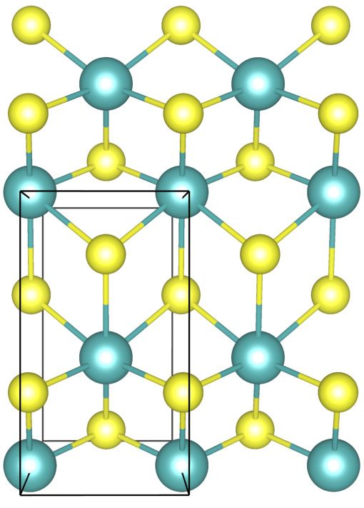
High-Throughput Computational Screening of Two-Dimensional Semiconductors
2

electronic properties. Finally, a short summary is given     structure at PBE level to determine the accurate po-
in Sec. V.                                                   sitions of both conduction-band minimum (CBM) and
                                                             valence-band maximum (VBM) in the reciprocal space.
                                                             It is well known that the PBE calculations provide suf-
                   II.   METHODOLOGY                         ficiently accurate results on forces (near equilibrium),
                                                             structures and band dispersion, but underestimates band
                                                             gaps. The HSE06 can well describes narrow or middle-
         A.    Density functional calculations
                                                             sized gap semiconductors, as long as their electronic
                                                             structures are not strongly localized.33 Considering that
   Our total energy and electronic structure calculations    the band structure calculations at HSE06 level is a rather
were performed using the Vienna Ab initio Simula-            time-consuming task, we only perform the static HSE06
tion Package (VASP).35,36 The electron-ion interaction       calculation at irreducible k-point coordinates but in-
was described using projector augmented wave (PAW)           cludes the positions of both CBM and VBM to determine
method37,38 and the exchange and correlation (XC)            more accurate band gap Eg values at the PBE-calculated
were treated with the generalized gradient approximation     lattice constants. Finally, if the candidate is thermody-
(GGA) in the Perdew Burke Ernzerhof (PBE) form39 . A         namically, mechanically and dynamically stable and has
cutoff energy of 400 eV was adopted for the plane wave       a HSE06 calculated band gap value larger than zero eV,
basis set, which yields total energies convergence better    this means that it might be a potential 2D semiconduc-
than 1 meV/atom. In addition, the non-bonding van der        tor. The purpose of this work is to identify the candi-
Waals (vdW) interaction is incorporated by employing a       dates of 2D semiconductors through large-scale screening
semi-empirical correction scheme of Grimme’s DFT-D2          of known materials, rather than to provide the most ac-
method in this study unless otherwise stated, which has      curate prediction of a specific 2D material.
been successful in describing the geometries of various
layered materials.40,41
   In the slab model of 2D systems, periodic slabs were                 III.   SCREENING CRITERIA
separated by a vacuum layer of 20 Å in c direction to
avoid mirror interactions. In sampling the Brillouin zone                A.    Thermodynamic Stability
integrations, we used Monkhorst-Pack k -point meshes
with a reciprocal space resolution of 2π×0.03 Å−1 .42
                                                                Thermodynamic stability describes the stability of a
On geometry optimization, both the shapes and in-
                                                             compound with respect to its decomposition into a set of
ternal structural parameters of pristine unit-cells were
                                                             competing phases, including elements and multicompo-
fully relaxed until the residual force on each atom is
                                                             nent compounds. To the best of our knowledge, three
less than 0.01 eV/Å. Considering that the band gaps
                                                             physical quantities are commonly use to evaluate the
of semiconductors are severely underestimated by tra-
                                                             thermodynamic stability of a free-standing 2D sheet,
ditional density functional theory (DFT) calculations
                                                             namely, exfoliation energy, energy convex hull and forma-
with local or semilocal exchange-correlation function-
                                                             tion energy. The exfoliation energy is the energy needed
als, part of electronic structure calculations were also
                                                             to exfoliate a monolayer from its bulk counterpart, which
performed using the standard Heyd-Scuseria-Ernzerhof
                                                             can evaluate the strength of interlayer bonds holding the
(HSE06) hybrid functional, namely, the screening pa-
                                                             layered bulk structure together. However, several 2D
rameter µ=0.2 Å−1 and the Hartree-Fock (HF) mixing
                                                             materials, such as borophene,47 lack any layered bulk
parameter α=25% respectively.32–34,43–45 Electronic cal-
                                                             structure from which they can be exfoliated. The en-
culations at the HSE06 level were performed upon the
                                                             ergy convex hull describes the competition between all
PBE-calculated equilibrium geometries.
                                                             different phases with the same compositions. Specifically,
                                                             the phases above the convex hull have a tendency to de-
                                                             compose into the ground state compounds phases on the
              B.    High-Throughput Setting                  convex hull. The definition of the energy convex hull
                                                             has the same problem as compared to the the exfolia-
   To screen the novel 2D semiconductors, we used the        tion energy.48,49 For example, the synthesis of 2D sheets
VASPKIT package46 as a high-throughput interface to          by mechanical exfoliation implies that is an endother-
pre-process the input files and post-process the calcu-      mic process to break the interlayer bonds. This means
lated data obtained by using VASP code. The overview         that all 2D materials with respect to their corresponding
of the screening process is presented in Fig. 1. Firstly,    bulk counterparts naturally fall above the convex hulls.
the code generates the other three input files (POTCAR,      The formation energy is defined as the difference between
KPOINTS, and INCAR) for a given structural POSCAR            a material and its pure elemental constituents in their
file. Then the spin-polarized structural-relaxation calcu-   ground states to evaluate its stability in the thermody-
lations at PBE-D2 level is performed to determine the        namic limit, namely,
magnetic ground state for each 2D material. If the can-                                      X
didate is nonmagnetic, we next perform the global band                        ∆Ef = Etot −       nα µα ,           (1)
High-Throughput Computational Screening of Two-Dimensional Semiconductors
3

                   2D structure databases
                                                                   worth noting that the accuracy of the PBE functional
                                                                   for the heat of formation is only around 0.2 eV/atom on
                                                                   average.50 Considering that semi-local functionals such
                                                                   as PBE generally underestimate the formation energies
                  Find the standard primitive cell                 of materials, especially for the layered materials. Thus,
                                                                   a universal threshold formation energy for the synthesis
                                                                   of 2D materials is not possible within the accuracy limits
    Perform spin-polarized calculation to optimize 2D structure
                           at PBE level
                                                                   of the existing XC functionals. We note that the PBE-
                                                                   calculated formation energies of Si, Ge and Sn monolayer
                                                                   are higher than 0.6 eV/f.u but they have recently been
                                No                                 synthesized or isolated by exfoliation.22,23,25 In our high-
        Non-magnetic?                For spintronic applications
                                                                   throughput screening process, we use a threshold of 1
                          Yes
                                                                   eV/formula-unit as an upper bound on sufficient thermo-
                                                                   dynamic stability for the synthesis and growth of free-
     Determine the locations of band edges (both VBM and
                      CBM) at PBE level
                                                                   standing monolayers.

               Determine band gap at HSE06 level                                   B.   Mechanical Stability
                       Semiconductor?
                                   Yes                                Mechanical stability describes the stability against de-
                                                                   formations or distortions in terms of strain. For a 2D
             Determine formation energy at PBE level
                   Thermodynamic stability?
                                                                   crystal, the relationship between the elastic constants
                                                                   and moduli can be given based on the Hooke’s law under
                                   Yes                             in-plane stress condition,51
            Determine elastic constants at PBE level                                                          
                    Mechanical stability?                                      σxx        C11 C12 C16        εxx
                                                                             σyy  =  C12 C22 C26   εyy ,
                                  Yes
                                                                               σxy        C61 C62 C66        2εxy
      Determine phonon spectrum using DFPT at PBE level
                    Dynamical stability?                           where C ij (i,j =1,2,6) is the in-plane stiffness tensor us-
                                                                   ing the standard Voigt notation: 1-xx, 2-yy, and 6-xy.
                                  Yes
                                                                   Generally, in first-principles calculations, the Cij can be
      Classify candidate based on symmetry and prototype           obtained based on the energy-strain method,52,53 namely,

FIG. 1. (Color online) Schematic representation of the funda-                    Eelastic (V, {εi }) = E(V, {εi }) − E (V0 , 0)
mental steps needed to find two-dimensional semiconductors.            1            1
                                                                     = C11 ε2xx + C22 ε2yy + C12 εxx εyy                        ,
                                                                       2            2
                                                                   +2C16 εxx εxy + 2C26 εyy εxy + 2C66 ε2xy
where Etot is the total energy of pristine 2D system                                                                         (2)
monolayer. n α is the number of atoms of species α and
µα is the atomic chemical potential of species α which is             where the tensile strain is defined as ε = a−a  a , a and
                                                                                                                        0

equal to the total energy of per atom in its most stable           a 0 are the lattice constants of the strained and strain-free
elemental phase. A negative value of ∆Ef for a mate-               structures. E (V, {εi }) and E (V0 , 0) are the total ener-
rial means that the thermodynamic stability. In other              gies of the equilibrium and distorted lattice cells, with
words, any processes that drive the transformation or              the volume of V and V0 , respectively. The elastic stabil-
decomposition of the this material are prohibitive or ki-          ity criterion of a crystalline structure requires the elastic
netically slow. For a material to be thermodynamically             energy, given by the quadratic form of Eq. 2, is always
stable, it must have a negative formation energy not only          positive in the harmonic approximation.
with respect to the pure constituents but relative to all             Obviously, the C ij is equal to the second partial deriva-
possible competing phases. Thus, a negative formation              tive of strain energy ES with respect to strain ε, and can
energy is a necessary but insufficient piece of evidence           be written as Cij = (1/S0 )(∂ 2 Eelastic /∂εi ∂εj ), where S0
for materials stability since the formation energy is the          is the equilibrium area of the system. Therefore, the unit
energy difference between a material and its pure elemen-          of elastic stiffness constants for 2D materials is force per
tal constituents. Considering that we mainly focus on the          unit length (N/m). In order to calculate the elastic stiff-
high throughput computational screening of 2D semicon-             ness constants, the Eelastic as a function of ε in the strain
ductors, we adopt the formation energy as the thermo-              range -2% 6 ε 6 2% with an increment of 0.5% are in-
dynamic stability criteria in our following study. It is           vestigated. The number of independent elastic constants
High-Throughput Computational Screening of Two-Dimensional Semiconductors
4

depends on the symmetry of a 2D crystal. For exam-             thermal stabilities is rather computationally expensive,
ple, the hexagonal crystals have two but the oblique ones      in our current study we use only the thermodynamic,
have 6 independent elastic constants. The number of in-        mechanical and dynamic stability criterions to screen the
dependent elastic constants as well as the necessary and       potential 2D materials.
sufficient elastic stability conditions for 2D lattice types
are summarized in Fig. 2.51,54
                                                                              D.   Semiconductor Screening

                 C.   Dynamic Stability                          The band gaps Eg of nonmagnetic semiconductors can
                                                               be obtained as,
   The dynamic stability reflects the structural tolerance
of a system against small atomic displacements, for ex-
ample, due to the thermal motions. It can be deter-                                Eg = CBM − VBM ,                  (3)
mined by calculating the phonon dispersions of a mate-
rial using either a finite displacement method55 or density       where CBM and VBM are the Kohn-Sham eigenvalues
functional perturbation theory56 . The dynamic stabil-         of CBM and VBM respectively. It is known that DFT-
ity of a material requires no imaginary phonon spectra         GGA severely underestimates the band gap of semicon-
existing in the phonon dispersions. For example, one           ductors but yield similar dispersion curves as compared
can find that no imaginary modes are observed in the           to the hybrid DFT result. Thus, we first perform the
phonon spectra of hexagonal MoS2 monolayer as showed           global band structure with a fine resolution of 2π×0.008
in Fig. 3 (a), implying that it is dynamically stable.         Å−1 (for example, a 59×59 kmesh for graphene), to lo-
Otherwise, the material will undergo reconstructive or         cate the positions of VBM and CBM for each potential
martensitic phase transformations after a slight lattice       candidate in the reciprocal-space at PBE level. Then we
distortion upon it. We derived phonon dispersions us-          calculate the values of both CBM and VBM at HSE06
ing the finite displacement approach as implemented in         level. There are five typical 2D Bravais lattices, namely,
the PHONOPY code.57 The force constants were derived           hexagonal, square, rectangular, centered rectangular and
from forces calculated on a supercell (both the lattice a      oblique respectively. The Ball-and-stick models, Bril-
and b larger than 20 Å) with atomic displacements of           louin zones and suggested k-paths for these Bravais lat-
0.01 Å along the lattice vectors.                              tices adopted in our high-throughput calculations are
   It is worth mentioning that small negative spectra, i.e.,   presented in Fig. 4 and Table I.
imaginary frequency near the Γ point is often observed
in the phonon spectra of 2D systems. As an illustrated
example, one can note that a small negative spectra near                IV.    RESULTS AND DISCUSSION
the Γ point appears in borophene monolayer sheet in Fig.
3 (c) which has been synthesized by recent experiments.47         Based on the above criteria, 97 direct- and 253 indirect-
Such small imaginary frequencies could be an artifact of       gap 2D nonmagnetic semiconductors are screened from
the convergence inaccuracy due to limited supercell size,      near 1000 2D monolayers. The PBE-calculated lattice
cutoff energy, or k-points; or they may reflect the actual     constants, formation energy, Young’s modulus, Poisson’s
lattice dynamical instability towards large wave undu-         ratio, as well as HSE06-calculated band gap, ionization
lations of 2D materials. It can possibly be eliminated         energy and electron affinity for each candidate are listed
by applying a small strain on the film or depositing the       in the Supplemental Material. Furthermore, the clas-
film onto a proper substrate.47,58 Thus, a candidate is        sification of these possible 2D semiconductors is sum-
still considered to be dynamically stable even if a tiny       marized in Fig. 5. One can find that the most of
imaginary frequency near the Γ point exists. It may            2D semiconductors are binary which is predominant by
be worth mentioning here that the phonon criterion is          AB2 structures. It should be pointed that transition-
still a necessary but not sufficient condition to evince dy-   metal dichalcogenides (TMDCs) is one of the most in-
namic stability of the material. Since the phonon analysis     teresting AB2 layered compounds and display a wide
deals only with small atomic displacements and cannot          range of important properties. The TMDCs monolayer
to capture phase transitions coupled with complex lattice      have three phases, namely, 2H (P-6m2), 1T (P-3m1)
reconstructions.49                                             and 1T’ (P21 /m) respectively. Previous theoretical stud-
   Finally, the thermal stability reflects the resistance to   ies predicted around 50 different transition-metal oxides
decomposition at high temperatures (higher than room           (TMOs) and TMDCs can remain stable as either 2H
temperature), which can be evaluated by performing             and/or 1T free-standing structures.59,60 Although part
ab-initio molecular dynamics simulations (AIMD) over           of these potential MX2 compounds are absent in their
a long time and wide range of temperatures. Strictly           bulk counterparts. For the sake of completeness, we
speaking, a stable material should satisfy thermody-           have also revisited the stability and electronic structure
namic, mechanical, dynamic and thermal stabilities si-         of TMOs and TMDCs with three possible phases (2H,
multaneously. Considering that the determination of            1T and 1T’ respectively). Furthermore, the most of these
High-Throughput Computational Screening of Two-Dimensional Semiconductors
5

           (a) Hexagonal                     (b) Square          (c) Rectangular       (d) Oblique

                                                                                                               Non-zero

                                                                                                                Zero

                                                                                                                   Equal

                                                                                                               1/2(C11-C12)

               C11 > 0,                   C11 > 0, C66 > 0,         C11 > 0,       C11 > 0, det(Cij) > 0,
              C11 > |C12|                   C11 > |C12|             C66 > 0        C11C22 > C12C12

     FIG. 2. Classification of crystal systems, independent elastic constants, elastic stability conditions for 2D materials.

                                    (a)                    (b)                         (c)                       (d)

FIG. 3. (Color online) Calculated (a) and (c) phonon dispersion curves, projected density of states (b) and (d) for H-MoS2 and
borophene sheet respectively.

TABLE I. Fractional coordinates of the specific points in reciprocal space for the four nonequivalent two-dimensional Bravais
lattices.
Bravais Lattice Label and coordinates of specific points Bravais Lattice Label and coordinates of specific points
                               Γ (0, 0)                                                 Γ (0, 0)
    Square                    X ( 12 , 0)                   Oblique                    X ( 12 , 0)
                              M ( 12 , 12 )                                            Y (0, 12 )
                               Γ (0, 0)                                                C ( 12 , 21 )
  Hexagonal                   K (3, 3)
                                  1 1
                                                            Oblique                   H (η, 1-ν)a
                              M ( 2 , 0)
                                   1
                                                                                     H1 (1-η, ν)a
 Rectangular                   Γ (0, 0)                   Rectangular                  X ( 12 , 0)
                              Y (0, 2 )1
                                                                                       S ( 12 , 12 )
         1−acosγ/b
          2sin2 γ ,                         and γ < 90°.
a                          1       ηbcosγ
    η=                ν=   2   −      a
High-Throughput Computational Screening of Two-Dimensional Semiconductors
6

                (a) Hexagonal                   (b) Square                (c) Rectangular            (d) Centered                   (e) Oblique
                                                                                                      Rectangular

                     a2
  2D Bravais              γ                                                                                                    a2
                          a1
  lattice
                                      a2                              a2                                a2
                                           γ                                γ                                γ                        γ
                                               a1                               a1                           a1                           a1

  2D Brillouin |a1|=|a2|, γ = 120o             |a1|=|a2|, γ = 90o          |a1|≠|a2|, γ = 90o      |a2|cosγ=1/2|a1|, γ ≠ 90o        |a1|≠|a2|, γ ≠ 90o
  zone                 M                                    M                        X   S
                                                                                                                  X H1
                                  K                                                                                  C                           X
                                                                                                                                                  H1
                                                            X                            Y                       Γ     H                   Γ      C
  Suggested                   Γ                        Γ                             Γ
                                                                                                                                               Y H
  2D k-paths
                    Γ-M-K-Γ                         Γ-X-M-Γ                Γ-X-S-Y-Γ                 Γ-X-H1-C-H-Γ               Γ-X-H1-C-H-Y-Γ

FIG. 4. (Color online) Overview of the five 2D Bravais lattices and corresponding Brillouin zones. The suggested k-paths for
band structure are indicated in blue line. The primitive unit cell is indicated in green box.

semiconducting candidates are found to have rectangular
or hexagonal Bravais lattices, and their band gap mag-
nitude is mainly concentrated between 1.0 eV and 3.0                                             ν(θ)/E(θ) = (S66 − S11 − S22 ) c2 s2
                                                                                                                                                         (5)
eV.                                                                                          −S12 c4 + s4 + (S26 − S16 ) cs3 − c3 s
                                                                                                                                   ,

                                                                                 and

               A.   Mechanical Properties
                                                                                         1/4G(θ) = (S11 + S22 − 2S12 ) c2 s2 +
                                                                                                    2                            ,                     (6)
                                                                                         S66 c2 − s2 /4 − (S16 − S26 ) c3 s − cs3
   We compare our predicted data with available ex-
perimental or theoretical reports. Up until now, sev-                            respectively, where s = sin(θ), c = cos(θ), and θ ∈
eral monolayers have been successfully exfoliated or                          [0, 2π] is the angle with respect to the +x axis. Sij =
synthesized in the experiments, including graphene                            C−1
                                                                                ij are elastic compliance constants. As an example,
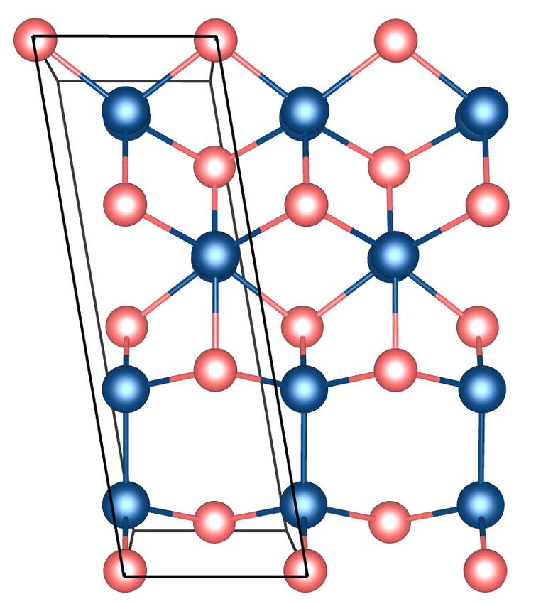
(P6/mmm),1 phosphorene (Pmna),12,16,17 borophene                              we present the orientation-dependent Youngs’s modulus
(Cmmm),47 BN (P-6m2)18,61 , MoS2 (P-6m2)14 , TiS3                             Y (θ), Poisson’s ratio ν(θ) and shear modulus G(θ) for
(P2_1/m)62 . We summarize the calculated in-plane elas-                       phosphorene sheet in Fig. 6. One can find that the elastic
tic stiffness constants, the minimum and maximum of                           prosperities of phosphorene show strong anisotropicity.
Youngs’s modulus, shear modulus and Poisson’s ratio
for these systems in Table II. One can find that our
predicted results are well agreement with the available                                            B.    Electronic Properties
experimental and theoretical data. For example, the
PBE-calculated Young’s modulus and Poisson’s ratio of
                                                                                 In addition to energy gap (Eg ), ionization energy (IE)
graphene are 339 N/m and 0.17, in excellent agreement
                                                                              and electron affinity (EA) are important parameters for
with the available values of 340 N/m and 0.186,63,64 re-
                                                                              any electronic material. They can be calculated by align-
spectively. To investigate the elastic anisotropy of 2D
                                                                              ing VBM and CBM with respect to the vacuum level.
materials, we also calculated the orientation-dependent
                                                                              The latter is also determined by aligning the planar-
Young’s moduli Y (θ) and Poisson’s ratio ν(θ) and shear
                                                                              averaged Hartree potential within the layer with the vac-
modulus G(θ) using the following formulae,65,66
                                                                              uum region as illustrated in Fig. 7. We take graphene as
                                                                              an example and present its global band structure in Fig.
                                                                              9 (a). It is clearly found that the band edges, i.e., both
           1/E(θ) = S11 c4 + S22 s4 + 2S16 c3 s
                                               ,                    (4)       the VBM and CBM encounter at the K point (1/3, 1/3)
               +2S26 cs3 + (S66 + 2S12 ) c2 s2                                to form the Dirac cone. By analyzing the projected band
                                                                              structure and the real-part of wave functions of band
  and                                                                         edges in real space [Figs. 9 (b) and (d)], one can ob-
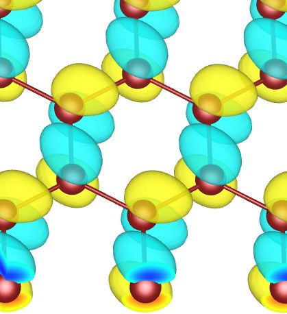
High-Throughput Computational Screening of Two-Dimensional Semiconductors
7

                   (a)                                        (b)                                      (c)

                   (d)                                      (e)                                        (f)

FIG. 5. (Color online) Classification of predicted two-dimensional semiconductors in term of (a) prototypes, (b) lattice type,
(c) Youngs’s modulus, (d) Poisson’s ratio, (e) band gap character and (f) band gap magnitude.

                      (a)                                     (b)                                      (c)

FIG. 6. (Color online) Calculated orientation-dependent (a) Youngs’s modulus E(θ), (b) Poisson’s ratio ν(θ) and (c) shear
modulus G(θ) for phosphorene respectively.

TABLE II. PBE-calculated in-plane elastic stiffness constants, Youngs’s modulus Y (θ), shear modulus G(θ) (in units of N/m),
and Poisson’s ratio ν(θ). For comparison purposes, the available theoretical or experimental values from the previous literature
are also shown.
                          C11                  C22                   C12             E(ϕ)           G(ϕ)             ν(ϕ)
  Systems         Calc.       Refs.    Calc.      Refs.      Calc.      Refs.    Max Min         Max Min          Max Min
 Graphene         349       342 [67]    349     342 [67]      60          -      339     339     144    144       0.17   0.17
Phosphorene       106       105 [68]    34       26 [68]      22       18 [68]    92      29      28     17       0.63   0.08
    BN            292       289 [67]    292     289 [67]      64          -      277     277     114    114       0.22   0.22
   MoS2           131       124 [69]    131     124 [69]      33          -      122     122      49     49       0.26   0.26
   TiS3            88        83 [69]    137     134 [69]      14          -      137      71      47     25       0.42   0.10
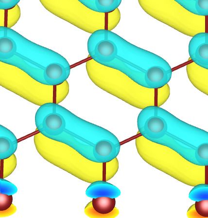
High-Throughput Computational Screening of Two-Dimensional Semiconductors
8

serve that the VBM and CBM to be derived from the                                 C.     Photocatalysis
bonding π and anti-bonding π ∗ states respectively, due
to the interaction of pz -pz orbitals of carbon atoms. In          Hydrogen generation by photocatalytic water splitting
addition, we also reproduce the semi-metallic character         presents a promising method for solar energy conversion.
of graphene, silicene and germanene, and stanene when           2D materials possess inherent advantages to improve
ignored the effect of spin-orbit coupling. The HSE06 cal-       photocatalytic performance for water splitting because of
culated band gap of 1.61 eV for phosphorene, 5.70 eV            their large surface-volume ratio and short diffusion dis-
for h-BN, 2.13 eV for MoS2 and 1.15 eV for TiS3 , well          tance for photo-generated electrons and holes.77–79 To
agreement with previous reports.14,18,70,71                     become a promising candidate semiconductor for water
                                                                splitting, three basic conditions need to be satisfied si-
                                                                multaneously: (i) the semiconductor must be insoluble
   Electron          Vacuum level
   energy                                                       in an aqueous solution; (ii) sufficient band gap must ex-
                                                                ceed the free energy of water splitting of 1.23 eV and be
                                                                smaller than around 3 eV to enhance solar absorption;
                                                                and (iii) proper band edge position must straddle the re-
                                                                dox potentials of water,80 namely, the position of CBM
                      IE   EA        WF                         must be more positive than the reduction potential of
                                                                H+ /H2 (-4.44 eV at pH=0) and the VBM must be more
                                                                than the oxidation potential (O2 /H2 ) (-5.67 eV at pH=0).
                                                                The redox potentials depend on the pH value in the
                                                                water splitting reaction. Specifically, the pH-dependent
              CBM
                                                                reduction potential for H+ /H2 and oxidation potential
               EF                                               for O2 /H2 are EH   + /H2 = −4.44eV + pH · 0.059eV and
                                                                                  red
                                Eg                              EO2 /H2 O = −5.67eV + pH · 0.059eV respectively.81
                                                                  ox

              VBM                                                  On the basis of these criteria, we extend the applica-
                                                                tions of the photocatalysis screening procedure to the 2D
                                                                semiconductors. We determine the band edge positions
                                                                relative to the vacuum level using the HSE06 as schemat-
                                                                ically shown in Fig. 7. Figure 11 compares the band edge
FIG. 7. (Color online) Schematic diagram of ionization energy   positions of 2D candidates for photocatalytic water split-
IE, electron affinity EA and work function WF defined as the    ting with the redox potentials at pH 0 or/and 7. Further
VBM, CBM and Fermi level EF with respect to the vacuum          details about the exact band edge values are given in the
level.                                                          Supplemental Material. Our computations show excel-
                                                                lent agreement with the previous reports. Interestingly,
   To analyze the anisotropic band dispersions near             Zhang and co-workers reported that the semiconductors
the VBM and CBM, we also provided the orientation-              with indirect band gap character are more suitable for
dependent effective mass m∗ (θ) and Fermi velocity νf (θ)       photocatalytic activity because the presence of different
of both holes and electrons for several candidates. As          k-vectors for the CBM and VBM in such cases reduces
illustrated examples, the PBE-calculated 2D polar rep-          the possibility of recombination of photogenerated elec-
resentation curves are presented in Fig. 10 respectively.       trons and holes.82
One can find that both the effective mass and Fermi
velocity curves at band edges for TiS3 monolayer show
highly anisotropic. Specifically, the calculated m∗ along                           V.    SUMMARY
Γ-X and Γ-Y are 0.32 (1.52) m0 and 1.06 (0.38) m0 for
hole (electron) in TiS3 monolayer, which are in good              In conclusion, we identified 93 direct- and 253 indirect-
agreement with previous results, 0.32 (1.47) m0 and 0.98        gap 2D nonmagnetic semiconductors from near 1000 2D
(0.41) m0 .72 Interestingly, the anisotropy of Fermi ve-        monolayers by performing high-throughput calculations
locity curves show an opposite trend. The calculated            together with density-functional theory. The calculated
effective mass ratios of hole γh (mxh divided by myh ) and      properties including lattice constants, formation energy,
electron γe (mxe divided by mye ) are 0.30 and 4.00, re-        Young’s modulus, Poisson’s ratio, band gap, band struc-
spectively, which show large anisotropy of effective mass       ture, ionization energy and electron affinity are available
when shifting the propagation direction from 0◦ (along          online for each candidate.
x axis) to 90◦ (along y axis). In contrast, the effective
mass of hole (electron) in MoS2 slightly increases from
0.54 (0.44) m0 along K-Γ to 0.61 (0.47) m0 along K-M                           ACKNOWLEDGMENTS
due to the higher hexagonal symmetry. The Fermi veloc-
ity of MoS2 monolayer is predicted to be around 0.5 ×             This work is supported by the support of Natural
105 m/s.                                                        Science Basic Research Plan in Shaanxi Province of
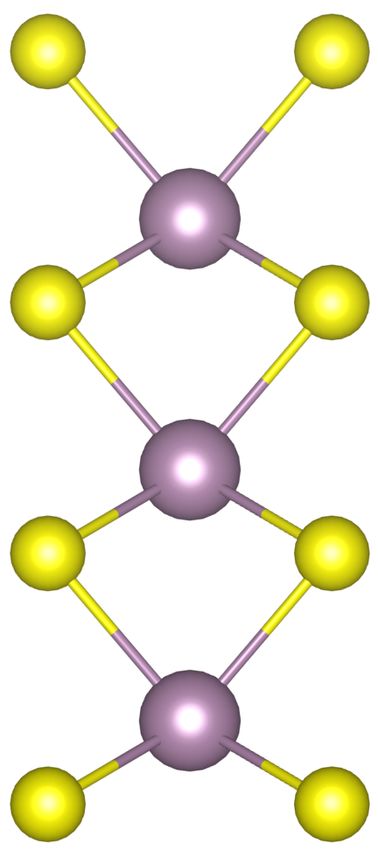
High-Throughput Computational Screening of Two-Dimensional Semiconductors
9

                            (a)                      (b)                                  (c)                     (d)

FIG. 8. (Color online) PBE calculated (a) global band structure in the vicinity of the Dirac point, (b) projected band structure,
(c) projected density of states, and (d) real part of wave function for band edges in graphene.

                    (a)                                    (b)                          (c)                      (d)

                                                                                                        Wavefunction@CBM

                3D Dirac cone
                                                                                                       Wavefunction@VBM

FIG. 9. (Color online) PBE calculated (a) global band structure in the vicinity of the Dirac point, (b) projected band structure,
(c) projected density of states, and (d) real part of wave function for band edges in graphene.

China (Program No. 2017JM1008), National Natural                  11604261) and by the Institute for Materials Research of
Science Foundation of China (Grant Nos. 11904285 and              Tohoku University for High Performance Computing.
High-Throughput Computational Screening of Two-Dimensional Semiconductors
10

                      (a)                                          (b)                                         (c)

FIG. 10. (Color online) PBE calculated orientation-dependent effective masses (in units of electron mass m0 ) and Fermi velocity
(in units of 105 m/s) of holes for (a, c) TiS3 and MoS2 and (b) electrons for TiS3 monolayers. The purple and blue lines indicate
the effective mass and Fermi velocity curves, respectively.

TABLE III. HSE06-calculated band gap, alignment of valence band maximum (VBM) and conduction band minimum (CBM)
with respect to the vacuum level. For comparison purposes, the available theoretical values from the previous literature are
also shown.
                            Band gap (eV)                      Ionization energy (eV)                      Electron affinity (eV)
 Material              Our work      Literature              Our work        Literature                  Our work        Literature
Phosphorene              1.57         1.52 [73]               -5.46           -5.43 [73]                  -3.89           -3.91 [73]
    BN                   5.71         5.68 [74]               -6.60           -6.56 [74]                  -0.89           -0.88 [74]
   MoS2                  2.18         2.15 [74]               -6.38           -6.33 [74]                  -4.20           -4.18 [74]
   WSe2                  2.04         1.98 [75]               -5.49           -5.82 [75]                  -3.45           -3.84 [75]
   TiS3                  1.15         1.06 [76]               -5.87           -5.34 [76]                  -4.72           -4.28 [76]

∗
    wangvei@icloud.com.                                                      M. G. Spencer, M. Terrones, W. Windl, and J. E. Gold-
†
    geng@ustb.edu.cn.                                                        berger, ACS Nano 7, 2898 (2013).
1                                                                        9
    K. S. Novoselov, A. K. Geim, S. V. Morozov, D. Jiang,                    Q. Zeng, H. Wang, W. Fu, Y. Gong, W. Zhou, P. M.
    Y. Zhang, S. V. Dubonos, I. V. Grigorieva, and A. A.                     Ajayan, J. Lou, and Z. Liu, Small 11, 1868 (2015).
                                                                     10
    Firsov, Science 306, 666 (2004).                                         S. Balendhran, S. Walia, H. Nili, S. Sriram,           and
2
    K. Novoselov, A. K. Geim, S. Morozov, D. Jiang, M. Kat-                  M. Bhaskaran, Small 11, 640 (2015).
                                                                     11
    snelson, I. Grigorieva, S. Dubonos, and A. Firsov, Nature                X. Wang, A. M. Jones, K. L. Seyler, V. Tran, Y. Jia,
    438, 197 (2005).                                                         H. Zhao, H. Wang, L. Yang, X. Xu, and F. Xia, Nat.
3
    L. Song, Z. Liu, A. L. M. Reddy, N. T. Narayanan, J. Taha-               Nano. 10, 517 (2015).
                                                                     12
    Tijerina, J. Peng, G. Gao, J. Lou, R. Vajtai, and P. M.                  H. Liu, Y. Du, Y. Deng, and P. D. Ye, Chem. Soc. Rev.
    Ajayan, Adv. Mater. 24, 4878 (2012).                                     44, 2732 (2015).
4                                                                    13
    Q. H. Wang, K. Kalantar-Zadeh, A. Kis, J. N. Coleman,                    H. Wang, H. Yuan, S. Sae Hong, Y. Li, and Y. Cui, Chem.
    and M. S. Strano, Nat. Nano. 7, 699 (2012).                              Soc. Rev. 44, 2664 (2015).
5                                                                    14
    Y. Zhang, Y.-W. Tan, H. L. Stormer, and P. Kim, Nature                   K. F. Mak, C. Lee, J. Hone, J. Shan, and T. F. Heinz,
    438, 201 (2005).                                                         Phys. Rev. Lett. 105, 136805 (2010).
6                                                                    15
    M. Chhowalla, H. S. Shin, G. Eda, L.-J. Li, K. P. Loh, and               S. Manzeli, D. Ovchinnikov, D. Pasquier, O. V. Yazyev,
    H. Zhang, Nat. Chem. 5, 263 (2013).                                      and A. Kis, Nat. Rev. Mater. 2, 17033 (2017).
7                                                                    16
    M. Xu, T. Liang, M. Shi, and H. Chen, Chem. Rev. 113,                    L. Li, Y. Yu, G. J. Ye, Q. Ge, X. Ou, H. Wu, D. Feng, X. H.
    3766 (2013).                                                             Chen, and Y. Zhang, Nat. Nanotechnol. 9, 372 (2014).
8                                                                    17
    S. Z. Butler, S. M. Hollen, L. Cao, Y. Cui, J. A. Gupta,                 H. Liu, A. T. Neal, Z. Zhu, Z. Luo, X. Xu, D. Tománek,
    H. R. Gutiérrez, T. F. Heinz, S. S. Hong, J. Huang, A. F.                and P. D. Ye, ACS Nano 8, 4033 (2014).
                                                                     18
    Ismach, E. Johnston-Halperin, M. Kuno, V. V. Plashnitsa,                 K. Watanabe, T. Taniguchi, and H. Kanda, Nat. Mater.
    R. D. Robinson, R. S. Ruoff, S. Salahuddin, J. Shan, L. Shi,             3, 404 (2004).
11

                                                       (a)                   0

                                                                                                                                                                                                                                                                                                     TeRhCl (Pm)
                                                                                                                                                                         PdS2 (P1)
                                                                                  GeP (P-6m2)
                                                                                                InSe (P3m1)
                                                                                                              SiP (P-6m2)
                                                                                                                            SnP (P-6m2)

                                                                                                                                                                                        PtSe2 (Pm)

                                                                                                                                                                                                                    RuSe2 (Pm)
                                                                                                                                                                                                                                 RhBr3 (P1)
                                                                                                                                                                                                                                              Bi2Se3 (Pm)
                                                                                                                                          MoS2 (P3m1)

                                                                                                                                                                                                                                                            Sb2S3 (Pm)
                                                                                                                                                                                                                                                                         PPdSe (P1)
                                                                                                                                                                                                                                                                                      PPdS (P1)

                                                                                                                                                                                                                                                                                                                   ZrBrN (Pmmn)
                                                                                                                                                                                                                                                                                                                                  CuTe2Br (P1)
                                                                                                                                                        OsSe2 (P2_1/m)

                                                                                                                                                                                                     PtSe2 (P3m1)

                                                                                                                                                                                                                                                                                                                                                 Bi2Te2Se (P3m1)
                                                                                                                                                                                                                                                                                                                                                                   Bi2Te2S (P3m1)
                                                                                                                                                                                                                                                                                                                                                                                    Nb3TeCl7 (P3m1)
                                                                                                                                                                                                                                                                                                                                                                                                      Ta3SeI7 (P3m1)
                                                                          −2

                                                      Energy level (eV)   −4
                                                                                          H+/H2
                                                                                                                                                                                           pH=0
                                                                                          O2/H2O
                                                                                                                                                         1.7                                                                                                                                                                          1.4
                                                                          −6                                                                                  I                      1.6                                                          1.7
                                                                                                                                                                                                                                               1.8 I 2.0                                                                           1.8 I 1.5   1.4
                                                                                                                                                                                                                                                                                                                                          I 1.7 D
                                                                                   2.2          2.2 I 2.2
                                                                                                                             2.2                                          2.2 1.9 1.9 I                                                                                                                                                I                                                D
                                                                                          I 2.3        D                                                                      I             I             I                                        I                           I 2.1 2.3
                                                                                             I   I                                                                                                                                                                                I   I
                                                                                                                                                                                                                                  2.9                                                                               2.9
                                                                                                                                                                                                                                     I                                                                                  D
                                                                          −8

                                                                                                         (b)                                                                                                                                                                                                                                              (c)
                          0                                                                                                                                                                               0

                                                                                                                                                                                                                                                                                                                                     SiP2 (Pm)

                                                                                                                                                                                                                                                                                                                                                                        AsI3 (P1)

                                                                                                                                                                                                                                                                                                                                                                                                                                     AlSiTe3 (Cm)
                                                                                                                                                                                                                    As (P-3m1)
                                                                                                                                                                                                                                  P (P-3m1)

                                                                                                                                                                                                                                                                                                                        PtI2 (P1)

                                                                                                                                                                                                                                                                                                                                                                                                                        TaI2O (Pm)
                                                                                                                                                                                                                                                              GaTe (P-6m2)
                                                                                                                                                                                                                                                                             SiAs (P-6m2)

                                                                                                                                                                                                                                                                                                           PdSe2 (P1)

                                                                                                                                                                                                                                                                                                                                                      WS2 (P3m1)

                                                                                                                                                                                                                                                                                                                                                                                                           P4Se5 (P1)

                                                                                                                                                                                                                                                                                                                                                                                                                                                                                    Al3Te3I (Pm)
                                                                                                                                                                                                                                               GaSe (P-6m2)

                                                                                                                                                                                                                                                                                            MoSe2 (P3m1)

                                                                                                                                                                                                                                                                                                                                                                                                                                                    MgPSe3 (P1)
                                                                                                                                                                                                                                                                                                                                                                                         As4S3 (P2_1/m)

                                                                                                                                                                                                                                                                                                                                                                                                                                                                  PdSeO3 (P2_1/m)
                              As (P1)
                                        P (Pmna)
                                                   GeAs (P-6m2)
                                                                  InN (P1)

                                                                                                                                                                         TlPt2S3 (P1)
                                                                             SiH (P3m1)
                                                                                          SnAs (P-6m2)
                                                                                                         RuTe2 (Pm)
                                                                                                                      WSe2 (P3m1)
                                                                                                                                     Al2Te3 (P1)
                                                                                                                                                    HfIN (P3m1)

                                                                                                                                                                                                     −2
                         −2
     Energy level (eV)

                                                                                                                                                                                                     −4 H+/H                                                                                                                                                                                                                                                         pH=7
                                                                                                                                                                                                             2
                         −4
                                H+/H           2
                                                                                                           pH=7                                                                                         O2/H2O                                                                                                                                                                                                                                                      pH=0
                               O2/H2O                                                                                                                                                                                                                                                                                                                                                                                    1.8 2.0
                                                                                                          1.2                         2.4                                                            −6 2.2    2.1 2.1 2.0
                                                                                                                                                                                                                           2.2                                                                                                                                                                               2.5 I                                                                   2.7
                              1.4         1.6                                                                                                                                                            I                                                         I              I            D                    2.3     3.0                        2.4                                                                                I
                                D 1.6 1.6 D 2.8 1.7                                                           I        2.0                  I           1.7 2.4                                                                                 2.7                                                            I 2.5 D D        I                                                                                                                                                        I
                         −6        D   I      I  I                                                                          D                                                 I                                                    2.7 I                                                                          I      2.8 D                                                                                                                       3.0 2.9
                                                                                                                                                            I                                                                                                                                                                                                                                                                                                           I
                                                                                                                                                                                                                                      I                                                                                   D                                                                                                                            D

                                                                                                                                                                                                     −8

FIG. 11. (Color online) HSE06 calculated band edge positions of 2D candidates relative to the vacuum level for photocatalytic
water splitting at (a) pH 0, (b) pH 7 and (c) pH 0-7. The redox potentials of water splitting at pH 0 (red dotted line) and pH
7 (green dashed line) are shown for comparison.

19
     Y. Sugiyama, H. Okamoto, T. Mitsuoka, T. Morikawa,                                                                                                                                                                                                 1020 (2015).
                                                                                                                                                                                                                                               26
     K. Nakanishi, T. Ohta, and H. Nakano, JACS 132, 5946                                                                                                                                                                                               T. Inoshita, S. Jeong, N. Hamada, and H. Hosono, Phys.
     (2010).                                                                                                                                                                                                                                            Rev. X 4, 031023 (2014).
20                                                                                                                                                                                                                                             27
     H. Okamoto, Y. Kumai, Y. Sugiyama, T. Mitsuoka,                                                                                                                                                                                                    M. Ashton, J. Paul, S. B. Sinnott, and R. G. Hennig,
     K. Nakanishi, T. Ohta, H. Nozaki, S. Yamaguchi, S. Shirai,                                                                                                                                                                                         Phys. Rev. Lett. 118, 106101 (2017).
                                                                                                                                                                                                                                               28
     and H. Nakano, JACS 132, 2710 (2010).                                                                                                                                                                                                              A. Jain, S. P. Ong, G. Hautier, W. Chen, W. D. Richards,
21
     A. O?hare, F. Kusmartsev, and K. Kugel, Nano Lett. 12,                                                                                                                                                                                             S. Dacek, S. Cholia, D. Gunter, D. Skinner, G. Ceder, and
     1045 (2012).                                                                                                                                                                                                                                       K. A. Persson, APL Mater. 1, 011002 (2013).
22                                                                                                                                                                                                                                             29
     P. Vogt, P. De Padova, C. Quaresima, J. Avila,                                                                                                                                                                                                     K. Choudhary, I. Kalish, R. Beams, and F. Tavazza, Sci.
     E. Frantzeskakis, M. C. Asensio, A. Resta, B. Ealet, and                                                                                                                                                                                           Rep. 7, 5179 (2017).
                                                                                                                                                                                                                                               30
     G. Le Lay, Phys. Rev. Lett. 108, 155501 (2012).                                                                                                                                                                                                    N. Mounet, M. Gibertini, P. Schwaller, D. Campi,
23
     E. Bianco, S. Butler, S. Jiang, O. D. Restrepo, W. Windl,                                                                                                                                                                                          A. Merkys, A. Marrazzo, T. Sohier, I. E. Castelli, A. Ce-
     and J. E. Goldberger, ACS Nano 7, 4414 (2013).                                                                                                                                                                                                     pellotti, G. Pizzi, and N. Marzari, Nat. Nanotechnol. 13,
24
     L. Li, S.-z. Lu, J. Pan, Z. Qin, Y.-q. Wang, Y. Wang, G.-y.                                                                                                                                                                                        246 (2018).
                                                                                                                                                                                                                                               31
     Cao, S. Du, and H.-J. Gao, Adv. Mater. 26, 4820 (2014).                                                                                                                                                                                            P. M. Larsen, M. Pandey, M. Strange, and K. W. Jacob-
25
     F.-f. Zhu, W.-j. Chen, Y. Xu, C.-l. Gao, D.-d. Guan, C.-h.                                                                                                                                                                                         sen, Phys. Rev. Materials 3, 034003 (2019).
     Liu, D. Qian, S.-C. Zhang, and J.-f. Jia, Nat. Mater. 14,
12

32                                                                  60
     J. Heyd, G. E. Scuseria, and M. Ernzerhof, J. Chem. Phys.           F. A. Rasmussen and K. S. Thygesen, J. Phys. Chem. C
     118, 8207 (2003).                                                   119, 13169 (2015).
33                                                                  61
     A. V. Krukau, O. A. Vydrov, A. F. Izmaylov, and G. E.               D. Pacilé, J. C. Meyer, Ç. Ö. Girit, and A. Zettl, Appl.
     Scuseria, J. Chem. Phys. 125, 224106 (2006).                        Phys. Lett. 92, 133107 (2008).
34                                                                  62
     M. Marsman, J. Paier, A. Stroppa, and G. Kresse, J.                 J. O. Island, M. Barawi, R. Biele, A. Almazán, J. M. Cla-
     Phys.: Condens. Matter 20, 064201 (2008).                           magirand, J. R. Ares, C. Sánchez, H. S. J. van der Zant,
35
     G. Kresse and J. Furthmüller, Phys. Rev. B 54, 11169                J. V. Álvarez, R. D’Agosta, I. J. Ferrer, and A. Castel-
     (1996).                                                             lanos?Gomez, Adv. Mater. 27, 2595 (2015).
36                                                                  63
     G. Kresse and J. Furthmüller, Comput. Phys. Sci. 6, 15              C. Lee, X. Wei, J. W. Kysar, and J. Hone, Science 321,
     (1996).                                                             385 (2008).
37                                                                  64
     P. E. Blöchl, Phys. Rev. B 50, 17953 (1994).                        F. Liu, P. Ming, and J. Li, Phys. Rev. B 76, 064120 (2007).
38                                                                  65
     G. Kresse and D. Joubert, Phys. Rev. B 59, 1758 (1999).             C. Jasiukiewicz, T. Paszkiewicz, and S. Wolski, physica
39
     J. P. Perdew, K. Burke, and M. Ernzerhof, Phys. Rev.                status solidi (b) 245, 562 (2008).
                                                                    66
     Lett. 77, 3865 (1996).                                              C. Jasiukiewicz, T. Paszkiewicz, and S. Wolski, physica
40
     S. Grimme, J. Comput. Chem. 27, 1787 (2006).                        status solidi (b) 247, 1247 (2010).
41                                                                  67
     T. Bučko, J. Hafner, S. Lebègue, and J. Ángyán, J. Phys.            A. Falin, Q. Cai, E. J. G. Santos, D. Scullion, D. Qian,
     Chem. A 114, 11814 (2010).                                          R. Zhang, Z. Yang, S. Huang, K. Watanabe, T. Taniguchi,
42
     H. J. Monkhorst and J. D. Pack, Phys. Rev. B 13, 5188               M. R. Barnett, Y. Chen, R. S. Ruoff, and L. H. Li, Nat.
     (1976).                                                             Commun. 8, 15815 (2017).
43                                                                  68
     A. D. Becke, J. Chem. Phys. 98, 1372 (1993).                        L. Wang, A. Kutana, X. Zou, and B. I. Yakobson,
44
     J. P. Perdew, M. Ernzerhof, and K. Burke, J. Chem. Phys.            Nanoscale 7, 9746 (2015).
                                                                    69
     105, 9982 (1996).                                                   J. Kang, H. Sahin, and F. M. Peeters, Phys. Chem. Chem.
45
     J. Paier, M. Marsman, K. Hummer, G. Kresse, I. C. Ger-              Phys. 17, 27742 (2015).
                                                                    70
     ber, and J. G. Angyan, J. Chem. Phys. 124, 154709                   V. Wang, Y. Kawazoe, and W. T. Geng, Phys. Rev. B 91,
     (2006).                                                             045433 (2015).
46                                                                  71
     V. Wang, N. Xu, J.-C. Liu, G. Tang, and W. Geng, arXiv              D. Jun, L. Ming, and Z. X. Cheng, WIREs Comput. Mol.
     preprint arXiv:1908.08269 (2019).                                   Sci. 6, 211 (2016).
47                                                                  72
     A. J. Mannix, X.-F. Zhou, B. Kiraly, J. D. Wood, D. Al-             Y. Jin, X. Li, and J. Yang, Phys. Chem. Chem. Phys. 17,
     ducin, B. D. Myers, X. Liu, B. L. Fisher, U. Santiago, J. R.        18665 (2015).
                                                                    73
     Guest, M. J. Yacaman, A. Ponce, A. R. Oganov, M. C.                 Y. Cai, G. Zhang, and Y.-W. Zhang, Scientific Reports 4,
     Hersam, and N. P. Guisinger, Science 350, 1513 (2015).              6677 (2014).
48                                                                  74
     J. T. Paul, A. K. Singh, Z. Dong, H. Zhuang, B. C.                  V. O. Özçelik, J. G. Azadani, C. Yang, S. J. Koester, and
     Revard, B. Rijal, M. Ashton, A. Linscheid, M. Blonsky,              T. Low, Phys. Rev. B 94, 035125 (2016).
                                                                    75
     D. Gluhovic, J. Guo, and R. G. Hennig, J. Phys.: Con-               J. Kang, S. Tongay, J. Zhou, J. Li, and J. Wu, Appl. Phys.
     dens. Matter 29, 473001 (2017).                                     Lett. 102, 012111 (2013).
49                                                                  76
     O. I. Malyi, K. V. Sopiha, and C. Persson, ACS Appl.                J. Dai and X. C. Zeng, Angew. Chem. Int. Ed. 54, 7572
     Mater. Interfaces 11, 24876 (2019).                                 (2015).
50                                                                  77
     M. Pandey and K. W. Jacobsen, Phys. Rev. B 91, 235201               A. K. Singh, K. Mathew, H. L. Zhuang, and R. G. Hennig,
     (2015).                                                             J. Phys. Chem. Lett. 6, 1087 (2015).
51                                                                  78
     M. Maździarz, 2D Mater. 6, 048001 (2019).                           X. Zhang, Z. Zhang, D. Wu, X. Zhang, X. Zhao, and
52
     L. D. Landau and E. M. Lifshitz, Course of Theoretical              Z. Zhou, Small Methods 2, 1700359 (2018).
                                                                    79
     Physics Vol 7: Theory and Elasticity (Pergamon press,               P. Ganguly, M. Harb, Z. Cao, L. Cavallo, A. Breen,
     1959).                                                              S. Dervin, D. D. Dionysiou, and S. C. Pillai, ACS En-
53
     Y. Le Page and P. Saxe, Phys. Rev. B 63, 174103 (2001).             ergy Letters 4, 1687 (2019).
54                                                                  80
     M. Born and K. Huang, “Dynamic theory of crystal lattice,           M. G. Walter, E. L. Warren, J. R. McKone, S. W.
     clarendon,” (1954).                                                 Boettcher, Q. Mi, E. A. Santori, and N. S. Lewis, Chem.
55
     K. Parlinski, Z. Q. Li, and Y. Kawazoe, Phys. Rev. Lett.            Rev. 110, 6446 (2010).
                                                                    81
     78, 4063 (1997).                                                    V. Chakrapani, J. C. Angus, A. B. Anderson, S. D. Wolter,
56
     S. Baroni, S. de Gironcoli, A. Dal Corso, and P. Giannozzi,         B. R. Stoner, and G. U. Sumanasekera, Science 318, 1424
     Rev. Mod. Phys. 73, 515 (2001).                                     (2007).
57                                                                  82
     A. Togo and I. Tanaka, Scr. Mater. 108, 1 (2015).                   P. Zhang, J. Zhang, and J. Gong, Chem. Soc. Rev. 43,
58
     E. S. Penev, A. Kutana, and B. I. Yakobson, Nano Lett.              4395 (2014).
     16, 2522 (2016).
59
     C. Ataca, H. ?ahin, and S. Ciraci, J. Phys. Chem. C 116,
     8983 (2012).
You can also read