How good are 2D transistors? An application-specific benchmarking study
←
→
Page content transcription
If your browser does not render page correctly, please read the page content below
Applied Physics Letters                                                                   PERSPECTIVE             scitation.org/journal/apl

    How good are 2D transistors? An
    application-specific benchmarking study
    Cite as: Appl. Phys. Lett. 118, 030501 (2021); doi: 10.1063/5.0029712
    Submitted: 15 September 2020 . Accepted: 4 January 2021 .
    Published Online: 21 January 2021

    Hattan Abuzaid,1               Nicholas X. Williams,1      and Aaron D. Franklin1,2,a)

    AFFILIATIONS
    1
        Department of Electrical and Computer Engineering, Duke University, Durham, North Carolina 27708, USA
    2
        Department of Chemistry, Duke University, Durham, North Carolina 27708, USA

    a)
         Author to whom correspondence should be addressed: aaron.franklin@duke.edu

    ABSTRACT
    The research community has invested heavily in semiconducting two-dimensional (2D) materials, such as transition metal dichalcogenides
    (TMDs). Their stability when scaled down to a few atoms thick makes them attractive candidates to replace or supplement silicon in many
    future technologies. Although this sentiment is prevalent, demonstrations of 2D field-effect transistors (FETs) often do not present their data
    in a way that enables a straightforward comparison. For example, some papers solely use mobility as the figure of merit, while others focus
    on unnormalized device on-current. Here, we benchmark the performance of a selection of 2D FETs with field-corrected metrics that allow a
    more accurate projection of their potential; while the demonstrated methods are by no means comprehensive, they provide insight into
    improved benchmarking of 2D FETs going forward. Importantly, we show that appropriate benchmarking requires consideration of the spe-
    cific application, with the three dominant potential application areas of front-end-of-line (FEOL) high-performance FETs, back-end-of-line
    (BEOL) 3D-integrated FETs, and low-cost thin-film FETs (or TFTs) each demonstrated. We find that 2D materials have the potential to
    compete with silicon as the channel in scaled FEOL high-performance devices. Meanwhile, in BEOL applications, FETs from in situ synthe-
    sized 2D materials have performance limited by their low crystal quality – a result of the stringent thermal budget of BEOL fabrication, which
    necessitates the use of transferred 2D materials. In the TFT area, 2D materials are simpler to fabricate than their silicon-based counterparts
    and they are competitive with other material alternatives. As promising as these findings are, there remain many hurdles for 2D materials to
    overcome, including poor reliability, performance variability, and fabrication scalability. Continuous research effort, combined with appro-
    priate benchmarking, is strongly encouraged.
    Published under license by AIP Publishing. https://doi.org/10.1063/5.0029712

          Semiconducting two-dimensional (2D) materials, including tran-      intrinsic quality of 2D channels14–19 even though devices with the
    sition metal dichalcogenides (TMDs) and X-enes such as black phos-        highest reported mobilities do not necessarily have the highest on-
    phorous (BP), are promising candidates for next-generation,               state performance in terms of on-current (ION).
    aggressively scaled field-effect transistors (FETs).1–3 Their layered            There are two main concerns for placing a high value on mobility
    nature preserves their general behavior down to a monolayer, and          in scaled, high-performance 2D transistors. First, the process of
    their atomic thinness enables excellent electrostatic gating control of   extracting field-effect mobility is known for being unreliable20,21 due
    the channel.4–9 Among 2D materials, the TMD, molybdenum disulfide         to the high contact resistance (forming at metal-2D interfaces),22–25
    (MoS2), stands out as a strong choice for n-type transistors toward       which dominates the total resistance of the device and obscures the
    complementary logic, as evidenced by the numerous experimental            intrinsic channel performance. Although most reports point to the
    demonstrations in the literature.10–13 Being the front-runner of 2D       likelihood of mobility underestimation, some also predict mobility
    FETs, high-performance MoS2 FETs are often employed as the indica-        overestimation from contact gating and other effects.26,27 These com-
    tor for progress of 2D FETs toward replacing or supplementing state-      plications manifest in a broad range of experimentally reported mobi-
    of-the-art silicon technology. However, published reports frequently      lities from as low as 0.02 cm2/(V s)28 to as high as 320 cm2/(V s)29 for
    make that comparison using metrics that touch upon limited aspects        monolayer MoS2. Second, because mobility describes the frequency of
    of device performance instead of forming a holistic picture. For exam-    scattering events during carrier transport, its relevance in ultra-scaled
    ple, mobility is widely used as an ultimate figure of merit for the       devices with ballistic channels is questionable.30 Altogether, these two

Appl. Phys. Lett. 118, 030501 (2021); doi: 10.1063/5.0029712                                                                                118, 030501-1
Published under license by AIP Publishing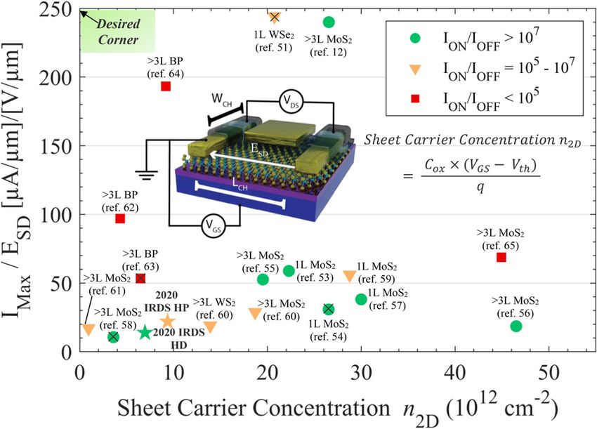
Applied Physics Letters PERSPECTIVE scitation.org/journal/apl
issues demonstrate that the widely adopted mobility metric is inade- thin-film transistors (TFTs), all of which have disparate processing
quate for singularly describing the promise of 2D FETs. and performance requirements (see Fig. 1). HP transistors power the
For evaluating the off-state performance of 2D devices, it is useful most demanding applications, like server chipsets or state-of-the-art
to look at the subthreshold swing (SS) and the on/off-current ratio CPUs—maximizing performance and minimizing size are of para-
(ION/IOFF).31–35 Nevertheless, these two metrics alone are not compre- mount importance in these applications.30 BEOL transistors are
hensive indicators. The IEEE International Roadmap for Devices and embedded during the final chip processing steps for added functional-
Systems (IRDS)36 specifies absolute current value requirements such ity or enhanced performance.39 By utilizing 3D monolithic integration,
that IOFF is small enough for an acceptable leakage power consump- BEOL transistors are added in the upper interconnect layers on top of
tion and ION is large enough for a sufficient switching speed. Hence, the finished front-end-of-line (FEOL) stack. Process compatibility is
ratios and swings are most meaningful when the terminal values are the main consideration for this device category because of the process
considered. Reporting ION as a measure for active device performance thermal budget and fabrication cost limits. Finally, TFTs sacrifice high
is a good starting point, but there needs to be a thoughtful normaliza- performance and miniaturization for low cost and versatility, with fab-
tion to enable comparison across various technology platforms and rication simplicity being a major requirement.30 TFTs are better suited
different device configurations. For instance, it is unrealistic to com- for applications like large-area and flexible electronics. An example of
pare the ION magnitude of a dual-gated, high-k dielectric encapsulated, improved benchmarking for each of these 2D device application areas
short-channel device with a SiO2 back-gated, long-channel one.37,38 It is provided herein, drawing from recently reported advances in the lit-
is also unmethodical to compare the performance of devices at largely erature, including from the Applied Physics Letters special collection.
disparate gate voltage overdrives (gate-source voltage minus threshold It has been a common practice to normalize ION by dividing it by
voltage, VGS – Vth) or drain-source voltages. the device width. Expressing ION in mA/lm or lA/lm makes it possi-
In addition to the important considerations for on- and off-state ble to correlate devices with an unequal width or integration density
performance metrics, it is also critical to focus on the most relevant and is a critical part of proper benchmarking; however, this normaliza-
deliverables for a particular application. 2D devices have been moti- tion is still insufficient for a straightforward comparison. Si FinFETs
vated as having broad applicability in the transistor space; yet, their are extremely miniaturized owing to state-of-the-art fabrication capa-
performance requirements differ significantly between areas from bilities, which are not available to scientists creating research-grade
high-performance computing to thin-film applications. The most nanoelectronics; thus, 2D FETs typically have longer channels. This
effective benchmarking approach must make appropriate comparisons device geometry disparity is still not captured by expressing current
among 2D device options while also putting these in the context of the per unit width. On the other hand, densely integrated, commercial Si
target application. FinFETs must adhere to the power density limit, which caps their
In this work, we propose and demonstrate a benchmarking drain-source voltage supply to a low value (0.7 V at the 5-nm technol-
approach utilizing relevant and cross-compatible metrics to investigate ogy node as per IEEE IRDS36), while 2D FETs are frequently reported
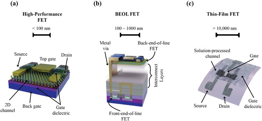
the potential of 2D materials for use in high-performance (HP) tran- with large drain-source voltages to display their saturation behavior or
sistors, back-end-of-line (BEOL, 3D-integrated) transistors, and compensate for their high total device resistance. We propose that
FIG. 1. Schematic illustration of different device applications where 2D materials can be employed. Scale bars indicate typical channel length dimensions. (a) HP transistor. (b)
BEOL transistor. (c) TFT.
Appl. Phys. Lett. 118, 030501 (2021); doi: 10.1063/5.0029712 118, 030501-2
Published under license by AIP Publishing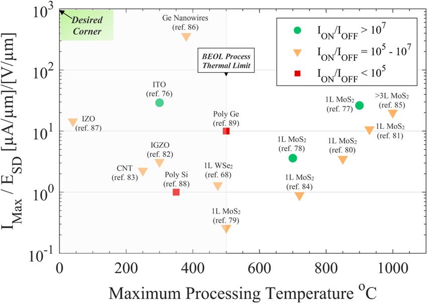
Applied Physics Letters                                                                                 PERSPECTIVE              scitation.org/journal/apl

    these disparities can be normalized through extracting ION from the                     basic, yet insightful, way to examine how devices with quite distinctive
    saturation regime and including the source-to-drain electric field (ESD)                dimensions and configurations compare to one another.
    averaged across the channel length, which is expressed in V/lm, in the                        The BP devices (Refs. 62–64) reported in Fig. 2 clearly outper-
    on-current metric. Hence, the maximum width-normalized on-cur-                          form silicon in terms of normalized drive current; unfortunately, they
    rent (IMax, lA/lm) over ESD has units of (lA/lm)/(V/lm) ¼ lA/                           suffer from a poor on/off-current ratio (less than 104 for these specific
    V ¼ lS. Although ION can also be extracted from the linear region,                      devices) due to the small bandgap of BP. This has been a fundamental
    that approach would introduce subjectivity into the selection of the                    limitation of BP along with its instability in air. There is still promise
    point of extraction (the point of highest IMax/ESD in the linear regime                 for BP as researchers tackle these problems,40–45 and further invest-
    could have impractically low ION). Devices that do not saturate will                    ment in BP is warranted due to its unique position as a proven p-type
    also have their performance exaggerated vs the ones that saturate as                    2D material.46 Quantum transport simulations on sub-10 nm mono-
    desired for logic transistors. While there are shortcomings to this                     layer BP FETs predict that they have the potential to meet the require-
    metric, including the nonuniformity of the electric field from source-                  ments of future technology nodes.47
    to-drain particularly in short-channel devices, the improvements it                           Another promising p-type material is WSe2, which unlike BP,
    provides in including the impact of applied fields and relative lengths                 has a sizable bandgap. WSe2 exhibits ambipolar conduction (having
    are considerable. This proposed benchmarking performance metric is                      similar electron and hole Schottky barriers) that can be pushed toward
    used throughout this paper to analyze the potential of 2D FETs in                       favorable hole transport using high-work function metals such as Pd
    each of the previously mentioned device categories.                                     and Au.48–50 The monolayer WSe2 device reported by Liu et al.51 com-
          To begin, we investigated 2D FETs targeted for applications as                    fortably exceeds 2020 IRDS HP requirements, albeit at a higher n2D.
    scaled, HP transistors. Benchmarking of the performance of a selection                  That result indicates hope for p-type 2D FETs to compete with current
    of HP 2D FET demonstrations is shown in Fig. 2 against the 2020                         technology. In comparison, n-type 2D FET demonstrations are domi-
    IEEE IRDS projection for Si FinFETs. IMax/ESD is presented (as                          nated by MoS2 as it is the highest-performing TMD thus far.52 The
    extracted from the saturation regime) with regard to the average sheet                  majority of MoS2 devices depicted in Fig. 2 had high ION/IOFF ratios
    carrier concentration in the channel, n2D ¼ Cox"(VGS – Vth)/q, where                    that met or exceeded the 2020 IRDS HD requirement. Notably, the
    Cox is the gate oxide capacitance and q is the elementary charge. The                   device demonstrated by Das et al.12 had substantial normalized
    use of n2D streamlines comparison of devices with a dissimilar gate                     drive current that outperformed its silicon counterpart. Further, that
    dielectric thickness, gate dielectric constant, gating configuration, and               device12 is still expected to maintain its superior position at the same
    gate voltage overdrive. Finally, the legend in Fig. 2 highlights the devi-              reduced n2D of IRDS projections. This is all assuming its current does
    ce’s on/off-current ratio. This whole benchmarking scheme provides a                    not saturate as its ESD increases (moving downward in the plot). This
                                                                                            assumption seems to be feasible considering that MoS2 FETs are pro-
                                                                                            jected to have Isat > 1 mA/lm for n2D # 20 " 1012 cm$2 at room tem-
                                                                                            perature.53 This is higher than the ION value of 0.854 mA/lm for 2020
                                                                                            IRDS HP.
                                                                                                  While this benchmarking example for HP 2D FETs is not com-
                                                                                            prehensive, it does have distinct advantages compared to traditional
                                                                                            approaches; for instance, if we were to use mobility as a sole perfor-
                                                                                            mance indicator, the device described by Liu et al.58—with a reported
                                                                                            field-effect mobility of 517 cm2/V s—would be deemed the best device
                                                                                            even though it has a low active on-state performance, as per the y-axis
                                                                                            in Fig. 2. This inflated mobility likely stems from an extraction error,
                                                                                            which is the main drawback for the adoption of mobility as a reliable
                                                                                            metric despite its appeal as a material-related property. It is important
                                                                                            to note that this benchmarking exercise ideally utilizes transistors that
                                                                                            are operating in the same regime. If all benchmarked devices had their
                                                                                            IMax/ESD extracted from the linear regime of the output characteristics,
                                                                                            then the relationship between the y-axis and the x-axis in the plot in
                                                                                            Fig. 2 would include isometric lines of constant mobility, which should
                                                                                            be extracted in the linear regime. However, most devices in Fig. 2 have
     FIG. 2. Performance benchmarking of a selection of 2D FET demonstrations in the        IMax/ESD extracted from the saturation regime, making their compari-
     category of HP transistors using the width-normalized on-current divided by the
     source-to-drain electric field vs the gate field-induced carrier concentration. 1 L:
                                                                                            son to the saturated silicon benchmarks reasonable and any compari-
     monolayer. >3 L: more than three layers thick. 2020 IRDS HP: IRDS projected            son to mobility unrealistic. Only the devices proposed by Zhang
     specifications for high-performance logic transistors at the 5 nm node. 2020 IRDS      et al.54, Liu et al.58, Liu et al.,51 and Wang et al.63 have metrics from
     HD: IRDS projected specifications for high-density or low-power logic transistors at   the linear regime, which could suggest that their performance is over-
     the 5 nm node. The data points with a superimposed “"” indicate cases where            estimated; nevertheless, their incorporation in the comparison does
     IMax/ESD was extracted from the linear region of the output characteristics (IDS vs    not alter the findings. The use of the IMax/ESD metric does carry the
     VDS) and, thus, may be exaggerated compared to the other points, which are from
     the saturation regime. Inset: schematic of a bottom-gated 2D FET (with an added        risk of negatively impacting devices where IMax is extracted at VDS
     top gate that is used in some reported devices) with key parameters                    > VDS,sat, particularly if the current truly does completely saturate (i.e.,
     highlighted.12,51,53–65                                                                zero output resistance). However, there are several factors that mitigate

Appl. Phys. Lett. 118, 030501 (2021); doi: 10.1063/5.0029712                                                                                                118, 030501-3
Published under license by AIP Publishing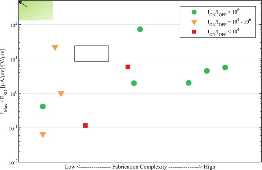
Applied Physics Letters                                                                               PERSPECTIVE               scitation.org/journal/apl

    this risk: (1) most 2D FETs do not completely saturate; (2) extraction                 either the device can be processed at a temperature below the process
    of IMax in the saturation regime is most often done just after VDS,sat                 limit (left side of figure) or (2) it can be grown with full coverage on a
    (true for all devices in Fig. 2 except for Bolshakov et al.61); and (3)                sacrificial substrate and subsequently transferred and patterned on the
    even when changing the extraction of IMax/ESD for the 5 nm node Si                     target chip (right side of the figure). The transfer approach appears to
    FinFETs to occurr at VDS ¼ Vt,sat, they still fall below 50 on the IMax/               be more promising for 2D materials due to the aforementioned tem-
    ESD axis, which is still below many of the 2D FET demonstrations.                      perature constraint. The BEOL stack performance requirement
    Overall, it is best if IMax is extracted as close to VDS,sat as possible for           depends on the FEOL stack it is integrated onto, and there is more
    this benchmarking approach, but it is also not absolutely critical.                    focus on functionality for this type of application. Therefore, it is more
    Hence, the use of this IMax/ESD vs n2D approach alleviates some of the                 informative to benchmark 2D FETs against other alternatives rather
    confusion stemming from incorrectly extracted mobility values and                      than a fixed roadmap projection.
    focuses more on on-current performance for a particular drain and                            The left-hand side of Fig. 3 (with maximum processing tempera-
    gate field, with some consideration of different channel lengths.                      tures
Applied Physics Letters PERSPECTIVE scitation.org/journal/apl
similar performance. While this says nothing of the challenges related
to synthesis, reproducibility, and process integration, at least from a
device performance Perspective, the vision is clearer with this bench-
marking approach.
A more feasible implementation for 2D materials in the nearer
term is in BEOL applications. However, the crystal quality of 2D mate-
rials suffers from the thermal constraint of a BEOL process. Ex situ
synthesis at higher temperatures and subsequent transfer appear to be
a promising route toward commercial implementation. With growing
interest in the added functionality of monolithic 3D-integrated devi-
ces, 2D materials are strong contenders for continuous consideration.
The advantageous properties of 2D materials and their compati-
bility with solution-phase processing make them a strong candidate
for TFTs. Their fabrication cost efficiency and satisfactory perfor-
mance in that category are a powerful combination. However, there
are many requisites for technological success that could not be cap-
FIG. 4. Performance benchmarking of a selection of 2D device demonstrations in tured in our analysis. 2D materials are notorious for their performance
the category of TFTs. a-IGZO: amorphous IGZO. a-Si: amorphous silicon. CNT: variability,108 and their scalable fabrication techniques are not
carbon nanotube. ALD: atomic layer deposition. Globally gated devices are indi-
cated as these would require additional fabrication complexity in order to achieve completely mature.85,109,110 A paradigm shift in current fabrication
local gates for virtually any application.97–107 approaches might be needed instead of striving to fit the mold of
incumbent methods. Nonetheless, the results reported so far by the
community of researchers are encouraging and they warrant substan-
steps to increase IMax/ESD. The same could be said about the in-place
tial investment into the betterment of this exciting class of semicon-
printed carbon nanotube (CNT) demonstration by Lu et al.98 It is
ductor materials. We propose that researchers perform more targeted
important to highlight that the devices reported by Gomes et al.,99 Xi
benchmarking in the analysis of their 2D devices, by considering the
et al.,97 and Higgins et al.100 were controlled using a global gate. While
impact of relative electric fields and focusing on the appropriate met-
that configuration is common in research demonstrations due to its
rics for a specific application.
simplicity, it is not viable in commercial circuits where individual con-
trol via a local gate is compulsory. Therefore, the fabrication complex- SUPPLEMENTARY MATERIAL
ity of these demonstrations might actually be higher if they follow that See the supplementary material for a detailed breakdown on fab-
mandate. Moreover, globally gated devices falsely enjoy lower contact rication complexity scoring for reported TFTs in Fig. 4.
resistance through the effect of contact gating. Consequently, their per-
formance is slightly exaggerated.6 The widely used amorphous silicon The authors would like to acknowledge the usefulness of the
(a-Si) (Refs. 102 and 103) provided reasonable performance yet suf- 2D Device Trends database (http://2d.stanford.edu/2D_Trends)
fered from a high fabrication complexity with a lengthy and compli- created by researchers in the Pop Lab at Stanford while preparing
cated procedure. Overall, 2D materials show some promise for TFT this work. This work was supported in part by the National Science
applications owing to their fabrication simplicity; however, there are Foundation (Grant No. ECCS-1915814). This work was performed
some key factors still to overcome in terms of reproducibility and scal- in part at the Duke University Shared Materials Instrumentation
ability of the processes. Hence, significant further research is needed to Facility (SMIF), a member of the North Carolina Research Triangle
optimize their processing to elevate their performance to viable levels. Nanotechnology Network (RTNN), which was supported by the
To summarize, we benchmarked the performance of 2D FETs National Science Foundation (Grant No. ECCS-1542015) as part of
across three distinct device categories using proposed, field-corrected the National Nanotechnology Coordinated Infrastructure (NNCI).
metrics. Our proposed scheme made it possible to compare devices
with a dissimilar structure and under varying bias conditions. Even DATA AVAILABILITY
though these benchmarking exercises were not exhaustive and do have The data that support the findings of this study are available
shortcomings, we were able to extract useful insight into the competi- from the corresponding author upon reasonable request.
tiveness of 2D-layered materials in distinct future technologies by
taking the specific needs of each technology into consideration. An REFERENCES
even more comprehensive approach to appropriate benchmarking 1
K. S. Novoselov, A. Mishchenko, A. Carvalho, and A. H. Castro Neto, Science
that may address lingering challenges with the approach herein would 353(6298), aac9439 (2016).
be welcome; in the meantime, the proposed benchmarking methods 2
W. Cao, J. Jiang, X. Xie, A. Pal, J. H. Chu, J. Kang, and K. Banerjee, IEEE
provide a distinct improvement over benchmarking with a single Trans. Electron Devices 65(10), 4109 (2018).
3
performance metric, such as unnormalized on-current or mobility. Y. Su, C. U. Kshirsagar, M. C. Robbins, N. Haratipour, and S. J. Koester, 2D
Mater. 3(1), 011006 (2016).
When 2D FETs are scaled down to the same dimensions as state- 4
Z. Ni, M. Ye, J. Ma, Y. Wang, R. Quhe, J. Zheng, L. Dai, D. Yu, J. Shi, and J.
of-the-art Si FinFETs, we expect them to be a viable contender in HP Yang, Adv. Electron. Mater. 2(9), 1600191 (2016).
transistors. MoS2 appears to be the front-runner for n-type devices, 5
R. Quhe, Q. Li, Q. Zhang, Y. Wang, H. Zhang, J. Li, X. Zhang, D. Chen, K.
while more work is needed to pinpoint a p-type material that offers Liu, and Y. Ye, Phys. Rev. Appl. 10(2), 024022 (2018).
Appl. Phys. Lett. 118, 030501 (2021); doi: 10.1063/5.0029712 118, 030501-5
Published under license by AIP PublishingApplied Physics Letters PERSPECTIVE scitation.org/journal/apl
6 43
Z. Cheng, K. Price, and A. D. Franklin, IEEE Trans. Electron Devices 65(10), X.-B. Li, P. Guo, T.-F. Cao, H. Liu, W.-M. Lau, and L.-M. Liu, Sci. Rep. 5,
4073 (2018). 10848 (2015).
7 44
H. Liu, A. T. Neal, and P. D. Ye, ACS Nano 6(10), 8563 (2012). B. Deng, V. Tran, Y. Xie, H. Jiang, C. Li, Q. Guo, X. Wang, H. Tian, S. J.
8
Y. Yoon, K. Ganapathi, and S. Salahuddin, Nano Lett. 11(9), 3768 (2011). Koester, and H. Wang, Nat. Commun. 8, 14474 (2017).
9 45
M. Perucchini, E. G. Marin, D. Marian, G. Iannaccone, and G. Fiori, Appl. J.-W. Jiang and H. S. Park, Phys. Rev. B 91(23), 235118 (2015).
46
Phys. Lett. 113(18), 183507 (2018). Q. He, Y. Liu, C. Tan, W. Zhai, G-h Nam, and H. Zhang, ACS Nano 13(11),
10
B. Radisavljevic, A. Radenovic, J. Brivio, V. Giacometti, and A. Kis, Nat. 12294 (2019).
47
Nanotechnol. 6(3), 147 (2011). R. Quhe, X. Peng, Y. Pan, M. Ye, Y. Wang, H. Zhang, S. Feng, Q. Zhang, J.
11
S. B. Desai, S. R. Madhvapathy, A. B. Sachid, J. P. Llinas, Q. Wang, G. H. Ahn, Shi, and J. Yang, ACS Appl. Mater. Interfaces 9(4), 3959 (2017).
48
G. Pitner, M. J. Kim, J. Bokor, and C. Hu, Science 354(6308), 99 (2016). H. Fang, S. Chuang, T. C. Chang, K. Takei, T. Takahashi, and A. Javey, Nano
12
S. Das, H.-Y. Chen, A. V. Penumatcha, and J. Appenzeller, Nano Lett. 13(1), Lett. 12(7), 3788 (2012).
49
100 (2013). P. M. Campbell, A. Tarasov, C. A. Joiner, M.-Y. Tsai, G. Pavlidis, S. Graham,
13
Y. Liu, J. Guo, Y. Wu, E. Zhu, N. O. Weiss, Q. He, H. Wu, H.-C. Cheng, Y. W. J. Ready, and E. M. Vogel, Nanoscale 8(4), 2268 (2016).
50
Xu, and I. Shakir, Nano Lett. 16(10), 6337 (2016). H. Zhou, C. Wang, J. C. Shaw, R. Cheng, Y. Chen, X. Huang, Y. Liu, N. O.
14
W. Bao, X. Cai, D. Kim, K. Sridhara, and M. S. Fuhrer, Appl. Phys. Lett. Weiss, Z. Lin, and Y. Huang, Nano Lett. 15(1), 709 (2015).
51
102(4), 042104 (2013). W. Liu, J. Kang, D. Sarkar, Y. Khatami, D. Jena, and K. Banerjee, Nano Lett.
15
J. Wang, Q. Yao, C. -W. Huang, X. Zou, L. Liao, S. Chen, Z. Fan, K. Zhang, 13(5), 1983 (2013).
52
W. Wu, and X. Xiao, Adv. Mater. 28(37), 8302 (2016). S. Zhang, S. T. Le, C. A. Richter, and C. A. Hacker, Appl. Phys. Lett. 115(7),
16
D. Jariwala, V. K. Sangwan, D. J. Late, J. E. Johns, V. P. Dravid, T. J. Marks, L. 073106 (2019).
53
J. Lauhon, and M. C. Hersam, Appl. Phys. Lett. 102(17), 173107 (2013). K. K. Smithe, C. D. English, S. V. Suryavanshi, and E. Pop, Nano Lett. 18(7),
17
W. Wu, D. De, S.-C. Chang, Y. Wang, H. Peng, J. Bao, and S.-S. Pei, Appl. 4516 (2018).
54
Phys. Lett. 102(14), 142106 (2013). Z. Zhang, X. Xu, J. Song, Q. Gao, S. Li, Q. Hu, X. Li, and Y. Wu, Appl. Phys.
18
H. Li, J.-K. Huang, Y. Shi, and L.-J. Li, Adv. Mater. Interfaces 6(24), 1900220 Lett. 113(20), 202103 (2018).
55
(2019). X. Zou, J. Wang, C.-H. Chiu, Y. Wu, X. Xiao, C. Jiang, W.-W. Wu, L. Mai, T.
19
J. Qiao, X. Kong, Z.-X. Hu, F. Yang, and W. Ji, Nat. Commun. 5(1), 4475 Chen, and J. Li, Adv. Mater. 26(36), 6255 (2014).
56
(2014). M. Si, C.-J. Su, C. Jiang, N. J. Conrad, H. Zhou, K. D. Maize, G. Qiu, C.-T.
20
H.-Y. Chang, W. Zhu, and D. Akinwande, Appl. Phys. Lett. 104(11), 113504 Wu, A. Shakouri, and M. A. Alam, Nat. Nanotechnol. 13(1), 24 (2018).
57
(2014). D. Lembke and A. Kis, ACS Nano 6(11), 10070 (2012).
21 58
M. S. Fuhrer and J. Hone, Nat. Nanotechnol. 8(3), 146 (2013). H. Liu and D. Ye Peide, IEEE Electron Device Lett. 33(4), 546 (2012).
22 59
S. McDonnell, R. Addou, C. Buie, R. M. Wallace, and C. L. Hinkle, ACS Nano C. J. McClellan, E. Yalon, K. K. Smithe, S. V. Suryavanshi, and E. Pop,
8(3), 2880 (2014). “Effective n-type doping of monolayer MoS2 by AlOx,” in 2017 75th Annual
23
F. Giubileo and A. Di Bartolomeo, Prog. Surf. Sci. 92(3), 143 (2017). Device Research Conference (DRC) (IEEE, 2017), pp. 1–2.
24 60
Y. Du, H. Liu, Y. Deng, and P. D. Ye, ACS Nano 8(10), 10035 (2014). L. Yang, K. Majumdar, H. Liu, Y. Du, H. Wu, M. Hatzistergos, P. Y. Hung, R.
25
D. Seo, D. Y. Lee, J. Kwon, J. J. Lee, T. Taniguchi, K. Watanabe, G.-H. Lee, K. Tieckelmann, W. Tsai, and C. Hobbs, Nano Lett. 14(11), 6275 (2014).
61
S. Kim, J. Hone, and Y. D. Kim, Appl. Phys. Lett. 115(1), 012104 (2019). P. Bolshakov, A. Khosravi, P. Zhao, P. K. Hurley, C. L. Hinkle, R. M. Wallace,
26
C. Liu, G. Li, R. Di Pietro, J. Huang, Y.-Y. Noh, X. Liu, and T. Minari, Phys. and C. D. Young, Appl. Phys. Lett. 112(25), 253502 (2018).
62
Rev. Appl. 8(3), 034020 (2017). H. Liu, A. T. Neal, Z. Zhu, Z. Luo, X. Xu, D. Tom"anek, and P. D. Ye, ACS
27
J. R. Nasr, D. S. Schulman, A. Sebastian, M. W. Horn, and S. Das, Adv. Mater. Nano 8(4), 4033 (2014).
63
31(2), 1806020 (2019). C.-H. Wang, J. A. C. Incorvia, C. J. McClellan, A. C. Yu, M. J. Mleczko, E.
28
Y.-H. Lee, X.-Q. Zhang, W. Zhang, M.-T. Chang, C.-T. Lin, K.-D. Chang, Y.-C. Pop, and H.-S. P. Wong, Nano Lett. 18(5), 2822 (2018).
64
Yu, J. T.-W. Wang, C.-S. Chang, and L.-J. Li, Adv. Mater. 24(17), 2320 (2012). L. Li, M. Engel, D. B. Farmer, S-j Han, and H.-S. P. Wong, ACS Nano 10(4),
29
B. Radisavljevic, M. B. Whitwick, and A. Kis, ACS Nano 5(12), 9934 (2011). 4672 (2016).
30 65
A. D. Franklin, Science 349(6249), aab2750 (2015). J. Kang, W. Liu, and K. Banerjee, Appl. Phys. Lett. 104(9), 093106 (2014).
31 66
Q. A. Vu, S. Fan, S. H. Lee, M.-K. Joo, W. J. Yu, and Y. H. Lee, 2D Mater. N. Briggs, S. Subramanian, Z. Lin, X. Li, X. Zhang, K. Zhang, K. Xiao, D.
5(3), 031001 (2018). Geohegan, R. Wallace, and L.-Q. Chen, 2D Mater. 6(2), 022001 (2019).
32 67
Y. Pan, K. Jia, K. Huang, Z. Wu, G. Bai, J. Yu, Z. Zhang, Q. Zhang, and H. D. Neumaier, S. Pindl, and M. C. Lemme, Nat. Mater. 18(6), 525 (2019).
68
Yin, Nanotechnology 30(9), 095202 (2019). A. Kozhakhmetov, J. R. Nasr, F. Zhang, K. Xu, N. C. Briggs, R. Addou, R.
33
S. Bhattacharjee, K. L. Ganapathi, S. Mohan, and N. Bhat, Appl. Phys. Lett. Wallace, S. K. Fullerton-Shirey, M. Terrones, and S. Das, 2D Mater. 7(1),
111(16), 163501 (2017). 015029 (2019).
34 69
C. Li, X. Yan, W. Bao, S. Ding, D. W. Zhang, and P. Zhou, Appl. Phys. Lett. D. Zhou, H. Shu, C. Hu, L. Jiang, P. Liang, and X. Chen, Cryst. Growth Des.
111(19), 193502 (2017). 18(2), 1012 (2018).
35 70
F. A. McGuire, Z. Cheng, K. Price, and A. D. Franklin, Appl. Phys. Lett. F. Chen and W. Su, CrystEngComm 20(33), 4823 (2018).
71
109(9), 093101 (2016). M.-W. Kim, J.-Y. Kim, Y.-H. Cho, H.-S. Park, and M.-K. Kwon, J. Nanosci.
36
See https://irds.ieee.org/editions/2020/more-moore for “IEEE International Nanotechnol. 18(3), 2140 (2018).
72
Roadmap for Devices and Systems 2020 Edition.” Z. Zhu, S. Zhan, J. Zhang, G. Jiang, M. Yi, and J. Wen, Mater. Res. Express
37
P. Bolshakov, P. Zhao, A. Azcatl, P. K. Hurley, R. M. Wallace, and C. D. 6(9), 095011 (2019).
73
Young, Appl. Phys. Lett. 111(3), 032110 (2017). J. Mun, Y. Kim, I.-S. Kang, S. K. Lim, S. J. Lee, J. W. Kim, H. M. Park, T. Kim,
38
D. Dev, A. Krishnaprasad, H. Kalita, S. Das, V. Rodriguez, J. C. Flores, L. and S.-W. Kang, Sci. Rep. 6(1), 21854 (2016).
74
Zhai, and T. Roy, Appl. Phys. Lett. 112(23), 232101 (2018). Y. Gong, Z. Lin, G. Ye, G. Shi, S. Feng, Y. Lei, A. L. El"ıas, N. Perea-Lopez, R.
39
S. Datta, S. Dutta, B. Grisafe, J. Smith, S. Srinivasa, and H. Ye, IEEE Micro Vajtai, and H. Terrones, ACS Nano 9(12), 11658 (2015).
75
39(6), 8 (2019). Y. Zhao, J.-G. Song, G. H. Ryu, K. Y. Ko, W. J. Woo, Y. Kim, D. Kim, J. H.
40
Y. Abate, D. Akinwande, S. Gamage, H. Wang, M. Snure, N. Poudel, and S. B. Lim, S. Lee, and Z. Lee, Nanoscale 10(19), 9338 (2018).
76
Cronin, Adv. Mater. 30(29), 1704749 (2018). S. Li, M. Tian, C. Gu, R. Wang, M. Wang, X. Xiong, X. Li, R. Huang, and Y.
41
Y. Y. Illarionov, M. Waltl, G. Rzepa, J.-S. Kim, S. Kim, A. Dodabalapur, D. Wu, “BEOL compatible 15-nm channel length ultrathin indium-tin-oxide
Akinwande, and T. Grasser, ACS Nano 10(10), 9543 (2016). transistors with Ion ¼ 970 lA/lm and on/off ratio near 1011 at Vds ¼ 0.5 V,”
42
S. P. Koenig, R. A. Doganov, H. Schmidt, A. H. Castro Neto, and B. in 2019 IEEE International Electron Devices Meeting (IEDM) (IEEE, 2019),
€
Ozyilmaz, Appl. Phys. Lett. 104(10), 103106 (2014). pp. 3–5.
Appl. Phys. Lett. 118, 030501 (2021); doi: 10.1063/5.0029712 118, 030501-6
Published under license by AIP PublishingApplied Physics Letters PERSPECTIVE scitation.org/journal/apl
77 93
X. Xu, G. Das, X. He, M. N. Hedhili, E. Di Fabrizio, X. Zhang, and H. N. X. Gao, G. Bian, and J. Zhu, J. Mater. Chem. C 7(41), 12835 (2019).
94
Alshareef, Adv. Funct. Mater. 29(32), 1901070 (2019). G. Hu, J. Kang, L. W. Ng, X. Zhu, R. C. Howe, C. G. Jones, M. C. Hersam,
78
C. J. McClellan, C. Y. Andrew, C.-H. Wang, H.-S. P. Wong, and E. Pop, and T. Hasan, Chem. Soc. Rev. 47(9), 3265 (2018).
95
“Vertical sidewall MoS2 growth and transistors,” in 2019 Device Research Z. Zhu, I. Murtaza, H. Meng, and W. Huang, RSC Adv. 7(28), 17387 (2017).
96
Conference (DRC) (IEEE, 2019), pp. 65–66. C. Tan, Z. Liu, W. Huang, and H. Zhang, Chem. Soc. Rev. 44(9), 2615
79
Y. Pan, H. Yin, K. Huang, Z. Zhang, Q. Zhang, K. Jia, Z. Wu, K. Luo, J. Yu, (2015).
97
and J. Li, IEEE J. Electron Devices Soc. 7, 483 (2019). Y. Xi, M. I. Serna, L. Cheng, Y. Gao, M. Baniasadi, R. Rodriguez-Davila, J.
80
K. A. Patel, R. W. Grady, K. K. Smithe, E. Pop, and R. Sordan, 2D Mater. Kim, M. A. Quevedo-Lopez, and M. Minary-Jolandan, J. Mater. Chem. C
7(1), 015018 (2019). 3(16), 3842 (2015).
81 98
H. Yu, M. Liao, W. Zhao, G. Liu, X. J. Zhou, Z. Wei, X. Xu, K. Liu, Z. Hu, and S. Lu, J. A. Cardenas, R. Worsley, N. X. Williams, J. B. Andrews, C. Casiraghi,
K. Deng, ACS Nano 11(12), 12001 (2017). and A. D. Franklin, ACS Nano 13(10), 11263 (2019).
82 99
K. Kaneko, N. Inoue, S. Saito, N. Furutake, H. Sunamura, J. Kawahara, M. F. O. V. Gomes, A. Pokle, M. Marinkovic, T. Balster, R. Anselmann, V.
Hane, and Y. Hayashi, “Highly reliable BEOL-transistor with oxygen-con- Nicolosi, and V. Wagner, Solid-State Electron. 158, 75 (2019).
100
trolled InGaZnO and gate/drain offset design for high/low voltage bridging I/ T. M. Higgins, S. Finn, M. Matthiesen, S. Grieger, K. Synnatschke, M.
O operations,” in 2011 International Electron Devices Meeting (IEEE, 2011), Brohmann, M. Rother, C. Backes, and J. Zaumseil, Adv. Funct. Mater. 29(4),
pp. 7–4. 1804387 (2019).
83 101
C.-C. Cheng, C.-C. Lu, T.-A. Chao, A.-S. Chou, H.-L. Chiang, T.-C. Chen, T. S. J. Lim, S.-J. Kwon, H. Kim, and J.-S. Park, Appl. Phys. Lett. 91(18), 183517
Gao, J. Zhao, Z. Cui, and L.-J. Li, “Monolithic heterogeneous integration of (2007).
102
BEOL power gating transistors of carbon nanotube networks with FEOL Si C.-M. Lee and B.-Y. Tsui, IEEE Electron Device Lett. 31(7), 683 (2010).
103
ring oscillator circuits,” in 2019 IEEE International Electron Devices Meeting J. H. Park, G. S. Jang, H. Y. Kim, S. K. Lee, and S. K. Joo, IEEE Electron
(IEDM) (IEEE, 2019), pp. 19.2.1–19.2.4. Device Lett. 36(9), 920 (2015).
84 104
P. Yang, X. Zou, Z. Zhang, M. Hong, J. Shi, S. Chen, J. Shu, L. Zhao, S. Jiang, M. Kim, J. H. Jeong, H. J. Lee, T. K. Ahn, H. S. Shin, J.-S. Park, J. K. Jeong, Y.-
X. Zhou et al., Nat. Commun. 9(1), 979 (2018). G. Mo, and H. D. Kim, Appl. Phys. Lett. 90(21), 212114 (2007).
85 105
I. Jahangir, G. Koley, and M. V. S. Chandrashekhar, Appl. Phys. Lett. C. J. Chiu, S. P. Chang, and S.-J. Chang, IEEE Electron Device Lett. 31(11),
110(18), 182108 (2017). 1245 (2010).
86 106
A. B. Greytak, L. J. Lauhon, M. S. Gudiksen, and C. M. Lieber, Appl. Phys. J. Yang, Y. Gu, E. Lee, H. Lee, S. H. Park, M.-H. Cho, Y. H. Kim, Y.-H. Kim,
Lett. 84(21), 4176 (2004). and H. Kim, Nanoscale 7(20), 9311 (2015).
87 107
Y.-L. Wang, F. Ren, W. Lim, D. P. Norton, S. J. Pearton, I. I. Kravchenko, and K. Xiong, L. Li, R. J. Marstell, A. Madjar, N. C. Strandwitz, J. C. Hwang, Z.
J. M. Zavada, Appl. Phys. Lett. 90(23), 232103 (2007). Lin, Y. Huang, X. Duan, and A. G€ oritz, IEEE Electron Device Lett. 39(9), 1453
88
A. Pecora, L. Maiolo, M. Cuscun#a, D. Simeone, A. Minotti, L. Mariucci, and (2018).
108
G. Fortunato, Solid-State Electron. 52(3), 348 (2008). W. Choi, D. Yin, S. Choo, S.-H. Jeong, H.-J. Kwon, Y. Yoon, and S. Kim,
89
T. Sadoh, H. Kamizuru, A. Kenjo, and M. Miyao, Appl. Phys. Lett. 89(19), Appl. Phys. Lett. 115(3), 033501 (2019).
109
192114 (2006). D. Kotekar-Patil, J. Deng, S. Liang Wong, C. Siong Lau, and K. E. J. Goh,
90
Q. H. Wang, K. Kalantar-Zadeh, A. Kis, J. N. Coleman, and M. S. Strano, Appl. Phys. Lett. 114(1), 013508 (2019).
110
Nat. Nanotechnol. 7(11), 699 (2012). J. Robertson, D. Blomdahl, K. Islam, T. Ismael, M. Woody, J. Failla, M.
91
J. Cheng, C. Wang, X. Zou, and L. Liao, Adv. Opt. Mater. 7(1), 1800441 (2019). Johnson, X. Zhang, and M. Escarra, Appl. Phys. Lett. 114(16), 163102
92
H. Zhan, D. Guo, and GXin Xie, Nanoscale 11(28), 13181 (2019). (2019).
Appl. Phys. Lett. 118, 030501 (2021); doi: 10.1063/5.0029712 118, 030501-7
Published under license by AIP PublishingYou can also read