How to Use Imaging Colorimeters to Correct OLED, MicroLED, and Other Emissive Displays for Improved Production Efficiency and Yields - WHITE PAPER
←
→
Page content transcription
If your browser does not render page correctly, please read the page content below
WHITE PAPER

How to Use Imaging Colorimeters to Correct
OLED, MicroLED, and Other Emissive Displays
for Improved Production Efficiency and Yields
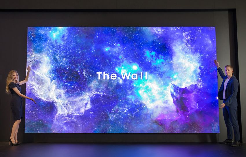
WHITE PAPER

How to Use Imaging Colorimeters to Correct
OLED, MicroLED, and Other Emissive Displays
for Improved Production Efficiency and Yields

Introduction
Emissive OLED, microLED (μLED), and miniLED are emerging as the next wave of
technology in the display market. This is exciting because these displays promise            Both OLEDs and microLEDs have

improved display performance and visual appearance with greater efficiency than other        superior contrast ratios and sharper

display technologies, thanks to their individually emitting pixel elements. Both OLEDs       images with deeper blacks and more

and microLEDs have superior contrast ratios and sharper images with deeper blacks            vibrant colors than LCDs. They require no

and more vibrant colors than traditional LCDs. These emissive displays require no            backlight, resulting in a thinner, lighter-

backlight, resulting in thinner, lighter-weight displays that use less electricity. OLEDs    weight display that uses less electricity.

also bring a dramatic boost in responsiveness, about 1,000 times faster than existing
technologies, virtually eliminating blur on fast-moving and 3D video. MicroLEDs match
OLED technology for response time and view-angle performance, but exceed OLED in
brightness and ruggedness, with even lower power consumption.

Figure 1 - The 219-inch microLED display “The Wall” by Samsung. (Source: Samsung)1

As manufacturers work to launch commercially viable emissive display products, high
costs due to material prices and manufacturing yield issues have hindered widespread
technology adoption—most dramatically in large-format implementations, as they drive
up end-customer prices. The smartphone market has been the most successful segment
for OLED technology to date and will likely be the catalyst that drives long-term adoption
of OLEDs and microLEDs for other applications. Display Supply Chain Consultants
(DSCC) cites smartphones as the dominant OLED market, accounting for around
91% of units per year with revenue share around 79% by 2022.2 Yole Développement
(Yole) projects a similar trend for microLEDs, with a longer ramp up period, and a
market reaching up to 330 million units by 2025.3 With this type of growth in demand,
improvements in manufacturing efficiency are needed.

2   I   Radiant Vision Systems, LLC
WHITE PAPER

Figure 2 - The smartphone market leads the way for OLED adoption. [Source: DSCC’s
Quarterly OLED Shipment and Fab Utilization Report]2

                                                                                          For both OLED and microLED, low
                                                                                          production yields due to manufacturing
                                                                                          complexity and—once manufactured—
                                                                                          visual quality issues impact the timing
                                                                                          of viable market entry and drive up retail
                                                                                          prices for finished display panels.

Figure 3 - Smartphones are similarly forecast to drive the microLED market. [Source:
Yole’s MicroLED Displays report]3

Although the near-term market size is small, analysts at DSCC predict that large-format
OLED TVs will take second seat to smartphones, rising to 42% market share by 2022,
overtaking LCDs by as soon as 2021.2 A limited sample of large-format microLED
displays have been showcased by manufacturers like Samsung (The Wall) and Sony
(Crystal-LED), whereas small-format displays continue to be more viable for mass

3   I   Radiant Vision Systems, LLC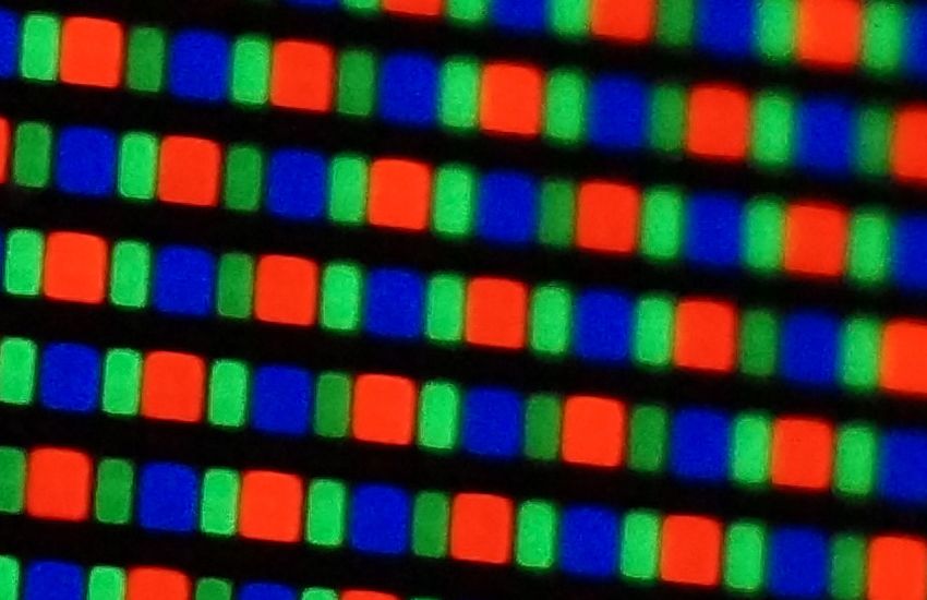
WHITE PAPER

production. For both OLED and microLED, low production yields due to manufacturing
complexity and—once manufactured—visual quality issues impact the timing of viable
market entry and drive up retail prices for finished display panels. Current commercially
available, large-format OLED TVs are priced into the thousands of dollars (USD), while
microLED screens remain cost prohibitive to most consumers, making lower-cost,
high-definition LCD and LED options more appealing to the budgets of price-minded
buyers. The price point for volume market adoption of new emissive display types and
replacement of current technologies must be significantly lower, demanding greater
efficiency and control in manufacture.

Display Manufacturing Challenges
OLED and microLED technologies add several unique challenges to the manufacturing
process, regardless of the size of display.

Large-format OLED screen manufacturing has been somewhat costly to date due to
inefficiency of deposition methods for adding organic molecules to their substrate (with
the exception of new inkjet printing methods), which has limited the application of OLED
technology primarily to smaller screen sizes like smartphones. Likewise, producing
an entire television screen out of microLED chips has so far proven to be challenging.
MicroLEDs require new assembly technologies, die structure, and manufacturing
infrastructure. For commercialization, fabricators must find methods that yield high
quality with microscopic accuracy while also achieving mass-production speeds. As
a point of comparison, a miniLED backlight screen may be made up of thousands of
individual miniLED units; a microLED screen is composed of millions of tiny LEDs.

To fabricate a microLED display, each individual microLED must be transferred to a
backplane that holds the array of units in place. The transfer equipment used to place
microLED units is required to have a high degree of precision, with placement accurate
to within ±1.5 µm. Existing pick & place LED assembly equipment can only achieve
±34 µm accuracy (multi-chip per transfer). Flip chip bonders typically feature accuracy
of ±1.5 µm—but only for a single unit at a time. Both of these traditional LED transfer
methods are not accurate enough for mass production of microLEDs.
                                                                                            It is necessary to measure and quantify
                                                                                            every pixel and subpixel element of an
There are also visual quality and performance issues. Inspecting OLED and microLED
                                                                                            emissive display to identify defects and
displays is in many ways more challenging than inspecting LCDs. Traditional LCD
                                                                                            ensure uniformity, to produce the level of
displays using LED backlights produce only a mostly uniform luminance (brightness)
                                                                                            quality that consumers expect at these
and color output across the display screen. With emissive display types, however, every
                                                                                            displays’ higher price points.
individual emitter in the display can be subject to a high a degree of variability. For
instance—although microLEDs are LEDs—traditional binning processes are virtually
impossible for microLEDs, which can be as small as 1/100th the size of a conventional
LED. Without these controls in place, ensuring brightness and color uniformity in
microLEDs can be extremely challenging. It is necessary to be able to measure and
quantify every pixel and subpixel element of an emissive display to identify defects
and ensure uniformity, to produce the level of quality that consumers expect at these
displays’ higher price points.

4   I   Radiant Vision Systems, LLC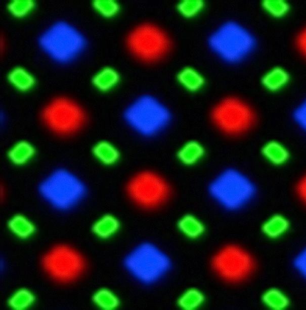
WHITE PAPER

Visual Quality Issues

Line Mura
In the OLED manufacturing process, material is deposited on a substrate to form the
individual subpixels, while extremely tiny microLEDs are transferred to backplanes
with the goal of achieving extreme precision. If this process is not completely uniform,
implications emerge in terms of visual quality. One such issue is line mura, which
appears as well-defined horizontal and/or vertical orientation in the display.

                                                                                               Extreme precision is needed to deposit
                                                                                               the individual emissive elements of a
                                                                                               display onto a substrate or backplane
                                                                                               to form the subpixel elements. If this
                                                                                               process is not completely uniform, the
                                                                                               end result may be line mura, which
                                                                                               appears as well-defined horizontal
                                                                                               and/or vertical orientation in the display.

Figure 4 - Image of an OLED display with uncorrected line mura.

Subpixel Luminance Performance
Emissive display pixels are composed of red, green, and blue subpixels. When current
is applied, each subpixel lights up individually, and the output of each subpixel is also
individually controlled. The brightness and color of each pixel in the display is determined
by combining the subpixel outputs. Due to production discrepancies in the manufacture
of emissive display types, there may be variations in luminance when the same electrical
signal is applied throughout the population of same-colored subpixels on the display. This
results in differences in brightness from pixel to pixel of the same color. When combined,
subpixels of each color—outputting light together at various brightness levels—produce
display pixels that exhibit even more variability in brightness and color, and consequently
the overall visual quality of the display appears poor.

Figure 5 - Subpixels combine to create pixels with various colors and brightness levels.

5   I   Radiant Vision Systems, LLC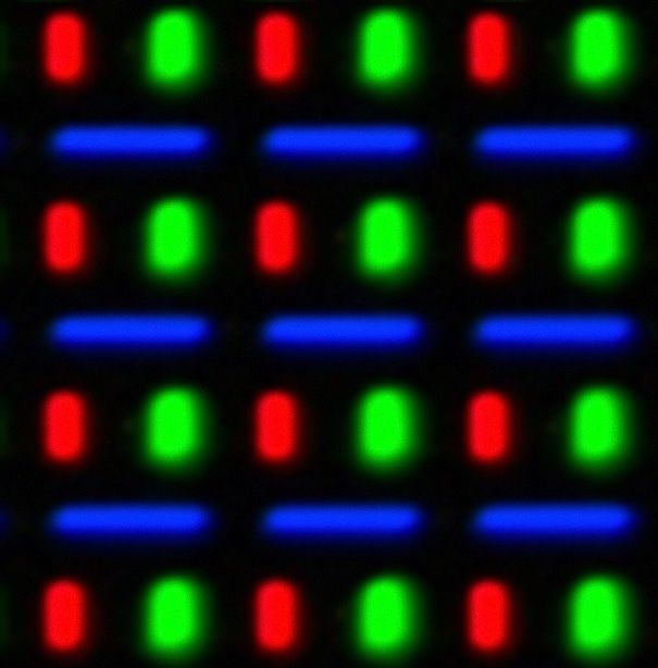
WHITE PAPER

This subpixel-level variability in OLED and other emissive displays results in different
performance issues than those that occur in LCDs. In LCD panels, all pixels rely on light
from the same backlight, so adjacent pixels generally have the same luminance and the
brightness across the display will be fairly uniform.

Color Nonuniformity
Another impact of inconsistent brightness levels at the display subpixels is reduced color
                                                                                                 To achieve accurate and uniform colors,
accuracy and color nonuniformity across the display. To achieve accurate and uniform
                                                                                                 the brightness of each individual subpixel
colors, the brightness of each individual same-colored subpixel must be tightly controlled.
                                                                                                 must be tightly controlled.
The reality is that even within a well-controlled manufacturing process, subpixels of emissive
displays will have significant variations in brightness levels. When these variations are not
compensated for, it may manifest as nonuniformity of color across the display, reducing
visual quality to potentially unacceptable levels and so reducing production yields.

Calibrated “White” display                         Uncalibrated “White” display
				                                               Green subpixel brightness is 10% too low

Figure 6 - Incorrect brightness levels create nonuniformity in color across an emissive
display. Variations in uniformity may increase as subpixels of various outputs are
combined to produce a single display color, such as white.

Imaging Colorimeter Applications for Emissive Displays
Imaging colorimetry-based display test systems have demonstrated success in improving
quality and reducing production costs for traditional LCD and LED display screens.
Testing applications span smartphones, tablets, laptops, TVs, and digital signage.
These proven techniques can be adapted to emissive display production testing as well,
enabling manufacturers to incorporate this technology into the same devices for visual
quality of OLED and microLED displays, with the same positive return on investment.

The two primary components of a display test system are:

1.       Imaging Colorimeters, which provide accurate measurement of display visual
         performance that matches human perception of brightness, color, and spatial (or
         angular) relationships. High-performance imaging colorimeters can accurately
         measure the luminance (brightness) of individual subpixels in an emissive display
         as well as overall display luminance and color uniformity.

6    I   Radiant Vision Systems, LLC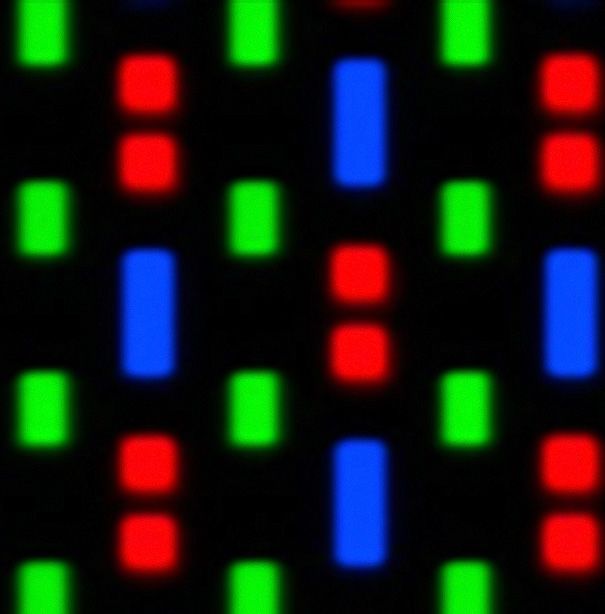
WHITE PAPER
2. Test Execution and Analysis Software, which is production-line software for
image analysis to identify defects and quality issues, quantify their magnitude, and
assess the measurements to make pass/fail determinations. This software can also
include display performance correction methods that can be adapted to identify
variabilities in subpixel output, calculate correction factors, and correct variations
that are unique to emissive displays.
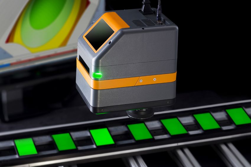
Figure 7 - Example of an imaging colorimeter in a production display test application.
(Product shown: Radiant Vision Systems ProMetric® I Imaging Colorimeter).
Improving End-of-Line Quality to Enhance
Customer Experience
In traditional manufacturing processes, display visual performance is tested by human
inspectors, resulting low control of the visual quality of delivered product. With the
innate variability, extremely high resolutions, and elevated quality expectations of
emissive displays, ensuring visual quality is becoming an even more significant issue.
Human inspectors are not able to consistently and repeatably evaluate the visual In traditional manufacturing processes,
qualities of these displays to an objective and quantitative level, which is necessary to display visual performance is tested by
determine overall performance. human inspectors, resulting low control of
the visual quality of delivered product.
Automated visual inspection (AVI) (also referred to as automated optical inspection
(AOI)) using imaging colorimeters has multiple benefits, elevating quality control
operations to increase efficiency in manufacturing, safeguard brand perception, and
ultimately enhance the user experience.
Benefits of automated display inspection using imaging colorimeters include:
• Improved consistency in display visual performance testing—from line to line,
and location to location—since all systems share the same calibration and test
definitions
7 I Radiant Vision Systems, LLC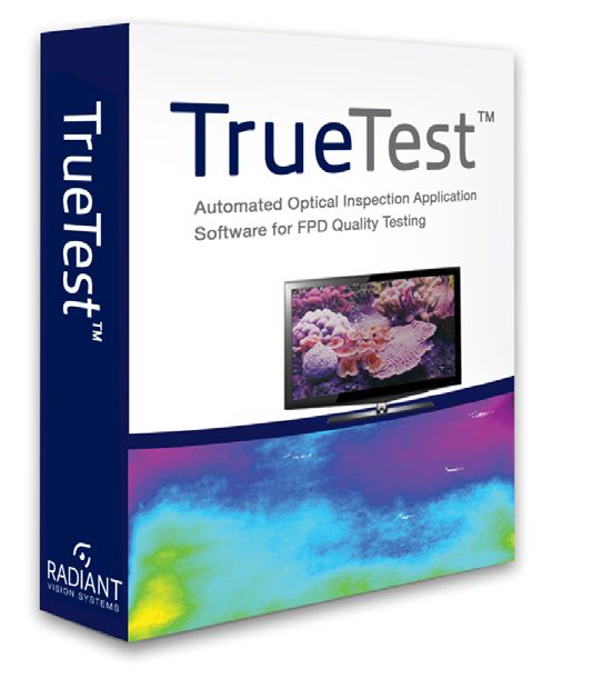
WHITE PAPER

     •     Quantitative assessment of defects, with precise tolerances for objectively
           “good” or “bad” displays (pass/fail)
     •     Increased testing speed, which allows more tests to be run within the same time
           interval, increasing throughput while ensuring a more careful assessment and a
           better end product
     •     Simultaneous assessment of contextual (full-display) quality inspection (e.g.,
           check uniformity and color accuracy) and fine-scale quality inspection (e.g.,
           detect pixel- and subpixel-level defects)

When applied in OLED and microLED display testing, imaging colorimeter-based AVI
simplifies testing while optimizing delivered product quality and production expense.

Correcting Emissive Displays to Improve Yield
As display size scales, yields decline drastically, and the cost of each component
is much higher. At a certain point it becomes viable for manufacturers to perform
correction (electronic compensation, or calibration) to improve display image quality.        As display size scales, yields decline
The concept is simple: by modifying the inputs to individual subpixels of an emissive         drastically, and the cost of each
display, previously identified dim subpixels can be adjusted to a uniform brightness          component is much higher. At a certain
level resulting in improved luminance uniformity and correct color across the display.        point it becomes viable for manufacturers
                                                                                              to perform correction (electronic
Display pixel uniformity correction requires, first, having in-display electronics that can   compensation, or calibration) to improve
control brightness of the individual subpixels and adjust this based on the calculated        display image quality.
correction factors for each subpixel. Second, a measurement system is required to
accurately quantify individual subpixel brightness and color, and compute specific
correction factors for each of them. This method has been widely used for LED display
screens made up of individual LEDs, and has been adapted for emissive displays like
OLED and microLED using a correction technique called “demura.”

Figure 8 - Side-by-side measurement images showing the results of a demura method
applied for correction of emissive displays, captured by a Radiant Vision Systems
ProMetric I Imaging Colorimeter; before demura (left) and after (right).

The demura method employs three distinct steps:

1.       Measurement of each subpixel in the display to calculate luminance values at
         each pixel location (performed on different test images to measure each series of
         same-colored subpixels) using a high-resolution imaging colorimeter.

8    I   Radiant Vision Systems, LLC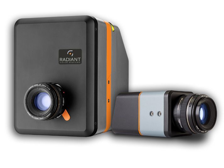
WHITE PAPER

2.       Calculation of correction factors needed to normalize luminance discrepancies
         between subpixels in the display using test analysis software.

3.       Application of correction factors to the display signals using an external control
         IC (integrated circuit) system.

Once a display is completely assembled, test images can be displayed on-screen to
target specific output color values. These images enable measurements and calibration
to be computed for each of these values. For example, a “green screen” with all green
subpixels turned on can be used as a sample image and the imaging colorimeter can
measure and record the brightness of each individual green subpixel. This is repeated          To adapt a measurement method for
for all the primary colors and, usually, white. This data can be gathered in the course of     any arbitrary size or resolution display,
ordinary quality testing of the emissive display.                                              a demura method may employ a
                                                                                               measurement process that combines
Calculating luminance values of each and every subpixel in extremely pixel-dense               data from a Spaced Pixel Test Pattern
OLED and microLED displays, however, can be challenging. For Full High Definition              analysis, a patented method that enables
(FHD, 1920 x 1080 pixel) and lower-resolution displays, a single 29-megapixel imaging          measurement using a single photometric
system offers sufficient resolution for testing. However, for higher-resolution displays       or colorimetric imaging system.
(for example, Quad High Definition or QHD, 4K, and now 8K), even very high-resolution
imaging systems may be unable to capture all pixels in a single image for complete
analysis, especially for today’s increasingly large displays (where a larger spatial area
must be measured). To overcome this challenge and adapt a measurement method for
any arbitrary size or resolution display, a demura method may employ a measurement
process that combines data from a Spaced Pixel Test Pattern analysis, a patented
method (US Patent 9135851 by Radiant Vision Systems) that enables measurement
using a single photometric or colorimetric imaging system.

Pattern 1			                               Pattern 2

Figure 9 - Examples of the first two patterns used in the Spaced-Pixel Test Pattern
method of pixel-level luminance measurement for extremely high-resolution displays.

Using a Spaced Pixel Test Pattern, dot matrix patterns of pixels are illuminated at
intervals and measured by the imaging system in multiple passes. Measurements are
repeated for all dot-matrix patterns until each display pixel is analyzed in its illuminated
state. When using an imaging system with sensor resolution higher than the display
itself, each display pixel can be tested over many sensor pixels, ensuring the highest
accuracy of the associated display pixel’s measured luminance value.

9    I   Radiant Vision Systems, LLC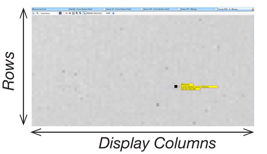
WHITE PAPER

Figure 10 - During the Space-Pixel Test Pattern method, each illuminated display
pixel is automatically registered by the analysis software and defined within a region of
interest (ROI). Because the imaging system resolution is much higher than the display
resolution, each display pixel may be measured across an ROI captured by multiple
sensor pixels, in this case about 10x10 sensor pixels to a single display pixel.

Once all patterns of illuminated pixels have been analyzed, the test and analysis
software of the demura solution combines all measurement images into a single
“synthetic image” with the same resolution as the measured display (one sensor pixel
to every display pixel). This image depicts every display pixel in rows and columns,
providing accurate x,y coordinates for each pixel and their associated luminance values.
This step in the demura process enables accurate detection of non-uniform pixels and
their exact coordinates where correction coefficients for luminance may be applied.

                                                                                            Figure 11 – Additionally, ROI are
                                                                                            dynamically defined regardless of OLED
                                                                                            subpixel layout or shape, meaning any
                                                                                            arbitrary pixel pattern can be measured to
                                                                                            apply demura to any display design.

Figure 12 - Software locates the defective pixels in the display using a synthetic image
that combines the data from multiple high-resolution measurement images of the
display, taken by the imaging system.

Once luminance values at each pixel are known, correction factors can be computed
and applied to the electrical input of each individual subpixel, ensuring that brightness
and color will be accurate and uniform across the entire display (including at all
gray levels). When this demura correction process is applied to the finished OLED
or microLED display, there is a significant improvement in display visual quality.
The net effect of demura is that displays that would have failed quality inspection
without electronic compensation will now be able to pass, thereby reducing waste in
manufacturing, improving cost efficiency, and increasing production yield.

10   I   Radiant Vision Systems, LLC
WHITE PAPER
The net effect of demura is that displays
that would have failed quality inspection
without electronic compensation will now
be able to pass, thereby reducing waste
and increasing production yield.
Figure 13 - Measurement images of a blue test screen on an OLED display, before and
after demura correction (shown in a false-color scale to illustrate luminance levels).
Radiant Vision Systems Solutions
Emissive technologies are ushering in the next generation of displays from flat-panel
to curved, but technical issues related to image quality and production yields need
to be resolved before display types like OLED and microLED can be considered
commercially viable, especially in large formats. The issues facing manufacturers—
although unique for emissive display types—are similar to technical issues that have
already been solved by Radiant Vision Systems in traditional LCD production and for
LED screens.
ProMetric® Imaging Colorimeters
Radiant Vision Systems ProMetric
Imaging Colorimeters are highly sensitive,
highly accurate, scientific-grade imaging
systems calibrated to match human
visual perception of spatial and angular
distributions of brightness and color.
Radiant Vision Systems offers more
than twice as many models of imaging
colorimeters as competitive solution
providers in the industry—with multiple options for resolution and sensitivity. The
appropriate system for specific display testing scenarios will depend on the desired The issues facing OLED manufacturers,
measurement accuracy and resolution requirements. although unique, are similar to technical
issues that have already been solved
TrueTest™ Software by Radiant Vision Systems in LCD
Accurate measurement of emissive display performance is important, but an equally- production and for LED screens.
important component is the analysis of the measurement data. Radiant Vision Systems
TrueTest Automated Visual Inspection (AVI) Software completes the display test solution
and makes data actionable by implementing test sequences against user-defined pass/
fail criteria. TrueTest is a software test suite and sequencer with built-in tests available
for display uniformity testing, line defect detection, pixel defect detection, contrast
11 I Radiant Vision Systems, LLCWHITE PAPER
measurement, mura analysis, and more. TrueTest
allows the user to select from a test library and
order tests in any sequence for rapid analysis of
multiple characteristics. The user can also specify
test parameters and pass/fail criteria. TrueMURA™
is an optional license for TrueTest that adds JND
(“just noticeable difference”) mura and blob analysis
techniques for evaluating over 15 types of mura.
TrueTest incorporates software alignment, display
registration, and moiré pattern removal functions
to simplify test setup. On the production line, the software runs in Operator mode
where access to test parameters is locked, preventing changes. TrueTest also stores
configuration information, test parameters, and pass/fail criteria for multiple models of
displays; the correct data file can be applied or changed on the fly during production.
Integration and Support
Practical implementation of the Radiant Vision Systems display test solution requires
both hardware and software integration on the production line. Radiant Vision Systems
is experienced at working with customer-selected fixture providers, or providing full
turnkey solutions that include fixtures. TrueTest Software can operate in a standalone
mode, but more typically it is integrated with the Production Control System (PCS) of
a manufacturer’s line. This integration can provide fully-automated testing, wherein
Radiant’s software is triggered by the PCS, or simply provides a reporting interface
for pass/fail results (and testing data). TrueTest can also be set up to work with video
pattern generators and barcode readers (or the equivalent).
Radiant Vision Systems offers global support for all ProMetric and TrueTest solutions.
Support includes engineering, installation, training, maintenance, and calibration
services. Radiant Vision Systems support personnel are located throughout the US,
China, Taiwan, Japan, Korea, Asia-Pacific, and Europe, supporting thousands of
imaging colorimeters currently deployed on hundreds of production lines worldwide.
References
1. Samsung. (2019, September 6). IFA 2019: Samsung Electronics celebra cinco
décadas de diseñar el futuro. Retrieved from: https://news.samsung.com/ar/ifa-
2019-samsung-electronics-celebra-cinco-decadas-de-disenar-el-futuro
2. DSCC. (2018, March). DSCC Releases Latest OLED Forecast. Retrieved from:
https://www.displaysupplychain.com/blog/dscc-releases-latest-oled-forecast
3. Yole Développement. (2017, February). MicroLED Displays report. Retrieved from:
http://www.yole.fr/MicroLEDDisplays_Market.aspx
12 I Radiant Vision Systems, LLCImaging colorimetry-based display test systems have demonstrated success
in improving quality and reducing production costs for LCD displays and
LED display screens. Radiant Vision Systems has extended these proven
techniques to production testing of other emissive displays like OLED and
microLED. Contact us to learn more about “demura” display correction and
how it can improve your production efficiency.
GLOBAL OFFICE LOCATIONS
Radiant maintains direct sales, engineering, and support offices and personnel throughout
North America, China, and Korea. Radiant is also sold and supported in other areas of the
world by our sister offices in the Konica Minolta Sensing Business.
AMERICAS EUROPE
Global HQ Radiant Vision Systems Europe HQ Nieuwegein, Netherlands
18640 NE 67th Ct.
Redmond, WA 98052 USA Regional Offices Diegem, Belgium
+1 425 844-0152 Paris, France
Info@RadiantVS.com Munich, Germany
Milan, Italy
Regional Offices Cupertino, California Wrocław, Poland
Novi, Michigan Vastra Frolunda, Sweden
Dietikon, Switzerland
Istanbul, Turkey
ASIA
Warrington, United Kingdom
China HQ Shanghai, China
Regional Offices Shenzhen, China
Suzhou, China
Japan Tokyo, Japan
Korea Seongnam, South Korea
Taiwan Zhubei, Taiwan
Asia-Pacific Singapore
Contact your local Radiant office at www.RadiantVisionSystems.com.
Copyright ©2020 Radiant Vision Systems LLC. All rights reserved. Specifications are subject to change without notice.
Radiant, Radiant Vision Systems, ProMetric, ProSource, VisionCAL, and Source Imaging Goniometer are registered
A Konica Minolta Company trademarks of Radiant Vision Systems LLC. 2020/01/29You can also read