Interface-engineering enhanced light emission from Si/Ge quantum dots
←
→
Page content transcription
If your browser does not render page correctly, please read the page content below
PAPER • OPEN ACCESS

Interface-engineering enhanced light emission from Si/Ge quantum dots
To cite this article: Zhi-Min Ji et al 2020 New J. Phys. 22 093037

View the article online for updates and enhancements.

                                 This content was downloaded from IP address 176.9.8.24 on 25/09/2020 at 19:02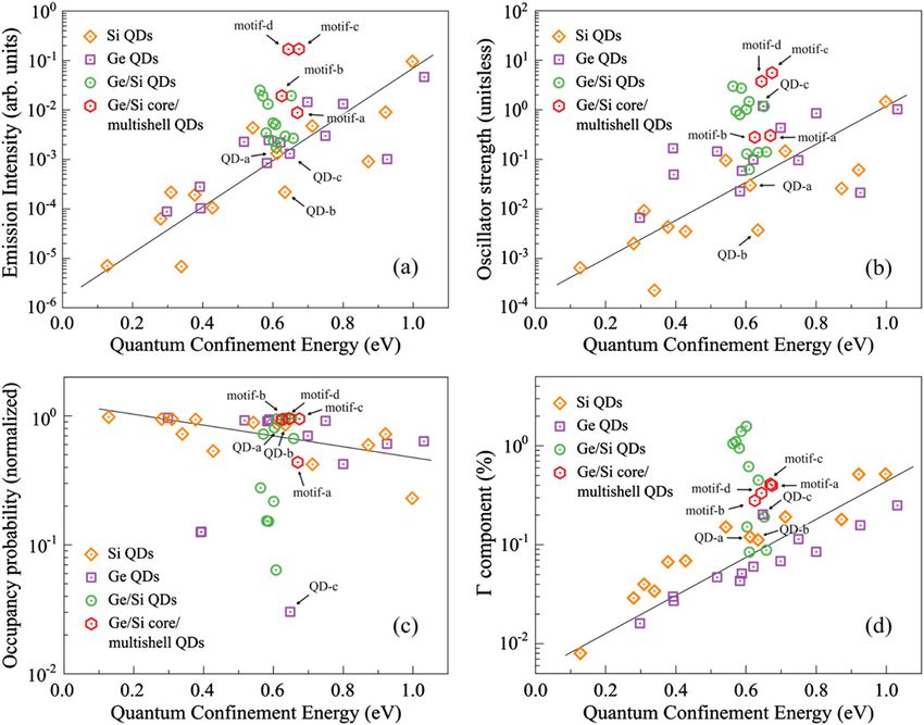
New J. Phys. 22 (2020) 093037                                                                 https://doi.org/10.1088/1367-2630/abafe7

                                 PAPER

                                 Interface-engineering enhanced light emission from Si/Ge
O P E N AC C E S S
                                 quantum dots
R E C E IVE D
15 May 2020
                                 Zhi-Min Ji1 , 2 , Jun-Wei Luo1 , 2 , 3 , 4    and Shu-Shen Li1 , 2
R E VISE D
                                 1
3 August 2020                        State Key Laboratory of Superlattices and Microstructures, Institute of Semiconductors, Chinese Academy of Sciences, Beijing
                                     100083, People’s Republic of China
AC C E PTE D FOR PUBL IC ATION   2
17 August 2020                       Center of Materials Science and Optoelectronics Engineering, University of Chinese Academy of Sciences, Beijing 100049, People’s
                                     Republic of China
PUBL ISHE D                      3
14 September 2020
                                     Beijing Academy of Quantum Information Sciences, Beijing 100193, People’s Republic of China
                                 4
                                     Author to whom any correspondence should be addressed.

Original content from            E-mail: jwluo@semi.ac.cn
this work may be used
under the terms of the           Keywords: silicon, germanium, quantum dot, interface effect, Γ -component, luminescence
Creative Commons
Attribution 4.0 licence.
Any further distribution
of this work must                Abstract
maintain attribution to
the author(s) and the            Si quantum dots (QDs) have a significant improvement in luminous efficiency compared with
title of the work, journal
citation and DOI.                bulk Si, achieved by alleviating the forbiddance of no-phonon Γ –Γ radiative transition
                                 determined by the law of momentum conservation. Two divergent mechanisms have been
                                 proposed to account for the breakdown of momentum conservation in Si QDs, one is due to the
                                 space-confinement-induced spread of k-space wave functions associated with Heisenberg
                                 uncertainty principle Δr · Δk > 1/2, and the other is due to the interface-effect-induced
                                 intervalley mixing between indirect and direct bandgap states. Both mechanisms could cause a
                                 small overlap of the electron and hole wave functions in k-space and make vertical transitions
                                 allowed, which leads to the zero-phonon light emission. In this work, we unravel the hierarchical
                                 relationship between these two primary mechanisms in the process of zero-phonon light emission
                                 from indirect bandgap QDs, by performing semiempirical pseudopotential calculation including
                                 many-body interaction on the room-temperature luminescent properties of a series of Si, Ge, and
                                 Ge/Si core/shell QDs. We show that the space confinement mechanism is dominant in both Si and
                                 Ge indirect bandgap QDs, and the interface-induced intervalley coupling mechanism plays a
                                 minor role. While in Ge/Si core/shell QDs, the interface-induced intervalley coupling mechanism
                                 has a more pronounced contribution to enhanced light emission, implying one can further
                                 enhance light emission via engineering interface based on the intervalley coupling mechanism.
                                 Given this, we further engineer the Ge QD interface by bringing four motifs of Si/Ge multiple
                                 layers from previously inverse designed Si/Ge superlattices and core/shell nanowires for light
                                 emitters. We show that two out of four motifs always give rise to two orders of magnitude
                                 enhancement in light emission relative to the Ge and Si QDs. We demonstrate that the interface
                                 engineering can enhance light emission in indirect bandgap QDs substantially and regulate the
                                 intervalley coupling mechanism as the primary factor over the space confinement mechanism in
                                 breaking the momentum conservation law.

                                 1. Introduction

                                 The discovery of visible photoluminescence (PL) from porous Si [1–3] and diverse types of Si
                                 nanostructures [4–8] has stimulated tremendous interest in their optical properties, which bear the hope of
                                 overcoming the inefficiency of light emission of bulk Si [9, 10] for developing Si-based light sources towards
                                 integrating both electronic and photonic devices on a single Si chip [10–15]. Bulk Si is an indirect bandgap
                                 material with the valence band maximum (VBM) at the Brillouin zone (BZ) center (i.e., Γ -point), like in
                                 the most semiconductors, whereas, the conduction band minimum (CBM) settled at six equivalent
                                 Δ-points at 0.85 × (2π/a0 ) from the Γ -point toward the X-point of the BZ (a0 ≈ 5.43 Å is the lattice

                                 © 2020 The Author(s). Published by IOP Publishing Ltd on behalf of the Institute of Physics and Deutsche Physikalische Gesellschaft
New J. Phys. 22 (2020) 093037                                                                                                     Z-M Ji et al

   Figure 1. (a) Diagrammatic sketch of the envelope functions of the highest-energy hole state and the lowest-energy electronic
   state along the Γ –X direction in k-space of Si QDs. (b) Schematic diagram of the electronic state energy levels in Si QDs. The six
   lowest unoccupied states are mainly composed of the six X-valleys of bulk Si transforming according to three irreducible
   representations (a1 , e, and t 2 ) under the operations of the point group T d . The triplet-degenerate t 2 state and the nondegenerate
   a1 state at the high energy position are folded by the Γ15 and Γ2  state of bulk Si, respectively. Coupling occurs between the
   electronic states with the same symmetry in QDs. (c) Band alignment of unstrained bulk Si and Ge. We take these values from
   empirical pseudopotential to the first principle calculations and the experimental data [34, 49]. Spin–orbit interaction is not
   taken into account. All energy levels are referenced to the VBM of bulk Si. Bandgap (Eg ) and direct–indirect bandgap energy
   difference (ΔEd – i ) are also marked in the figure.

constant of Si) [9]. For convenience, starting now, we refer Δ-valley to X-valley. In semiconductors, the free
electrons usually sit at the CBM and free holes at the VBM. As a result, the optical transitions are forbidden
unless phonons take part to supply the momentum difference between electron and hole to ensure the
momentum conservation [10]. Since the phonon-assisted transition is a second-order process with 4–5
orders longer in the radiative lifetime than the first-order zero-phonon radiative recombination as occurred
in the direct bandgap semiconductors [16], indirect bandgap semiconductors are not efficient light emitters.
Besides the frequently observed radiative recombination transitions related to surface defect states [17, 18],
it is now generally accepted that quantum confinement effect induced by the size reduction corresponds to
the observed light emission from Si nanostructures [18–25]. Despite over 30 years of intensive research, Si
nanostructure-based light source remains in its early stages for commercial applications, because Si
nanocrystals still behave as indirect semiconductors even though their luminous efficiency is superior to
bulk Si [20, 23].
     Two divergent mechanisms have been proposed to account for the quantum-confinement-induced
breakdown of the momentum-conservation rule in Si nanostructures [21, 24, 25]. One is the
space-confinement-induced spread of electron and hole in reciprocal space according to the Heisenberg
uncertainty principle Δr · Δk > 1/2 [19, 20]. The small overlap of the electron and hole wave functions in
k-space makes vertical transitions allowed (as illustrated in figure 1(a)), leading to the zero-phonon light
emission [19, 20]. We call this mechanism the space confinement mechanism. The other mechanism, which
we refer to as the intervalley coupling mechanism, is briefly described as follows. According to the zone
folding theory, the BZ of QD shrinks into a single Γ̄ -point, and all k-points in bulk BZ are folded onto this
Γ̄ -point [26, 27]. Once bulk Si X-valley folded onto Γ̄ -point, the surface potential of Si QD deviated from
the bulk Si crystal potential can probably induce mixing between the states belong to the same irreducible
representation derived from bulk Γ - and X-valley [23, 24, 28]. In this way, incorporating Γ -component
into the low-lying (in energy) X-derived QD electron states makes zero-phonon recombination with the
Γ -derived holes possible. The spherical Si QDs centered on a Si atom have the symmetry of the T d point
group [29–31]. The six lowest conduction band states folded from the six equivalent X-valleys of bulk Si
transform according to irreducible representations a1 (nondegenerate), e (twofold degenerate), and t 2
(threefold degenerate) of the T d point group (in the single group without considering spin–orbit coupling)
[29, 31]. Subsequently, the surface perturbation potential HQD of QDs couples X-derived electronic states
ψα (X) to high-lying Γ -derived electronic states ψα (Γ ) if they belong to the same representation α,
(here, α = a1 , e, t 2 ) [16]:

                                                  ψα (X) |HQD  |ψα (Γ )
                                        SαΓ −X =                          .                                  (1)
                                                        EΓ − E X

It is worth noting that without intervalley coupling (i.e., SαΓ −X = 0), the zone-folding alone does not break
the momentum conservation rule. The zero-phonon transition intensity is proportional to the
                    2
Γ -component SαΓ −X  in the X-derived QD electron state, which is inversely proportional to the square of
energy separation EΓ − EX between X-valley and Γ -valley in bulk Si. In this respect, Ge QDs are more
promising than Si QDs to archive high-efficiency light emission [32, 33]. In indirect bandgap Ge, the

                                                         2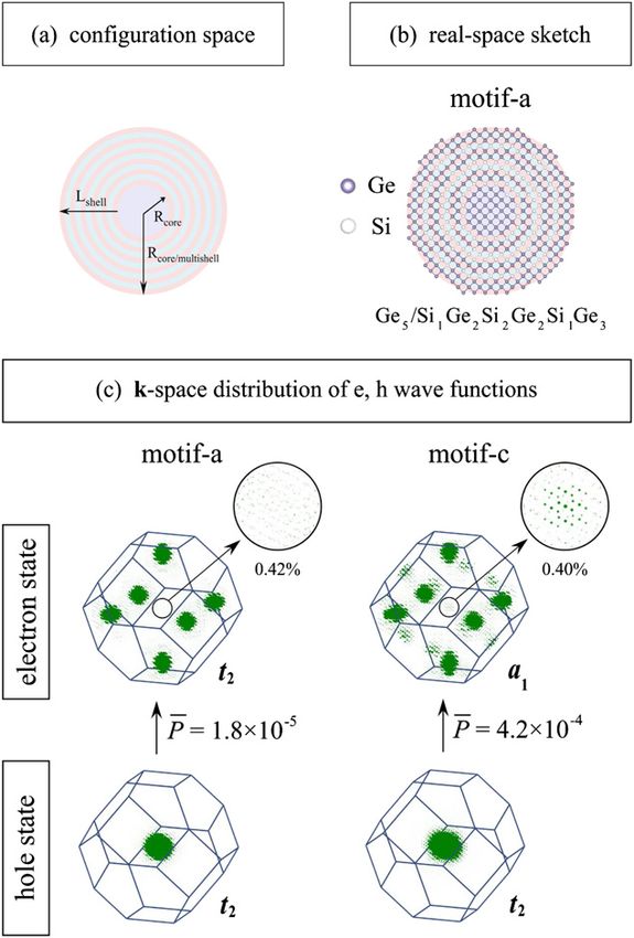
New J. Phys. 22 (2020) 093037                                                                                        Z-M Ji et al

indirect bandgap (L-valley) is fairly close to the direct bandgap (Γ -valley) with a small energy separation
EΓ − EL ≈ 0.14 eV relative to EΓ − EX ≈ 2.38 eV in Si (see reference [34], and figure 1(c)). Hence, even
when Ge QDs are relatively large, L- and Γ -valley are anticipated to be strongly coupled [35], giving rise to
intense zero-phonon transitions [33]. Unfortunately, such expected intense light emission in Ge QDs has
not been confirmed experimentally. Specifically, the reported radiative recombination lifetime is about 18
μs for 3.5 nm Ge QDs [33], and in a 1–1000 μs wide range for Si QDs depending on particle size [20, 36,
37]. This unexpected result is probably because other factors hinder the luminescence of Ge QDs, such as
the emission quenching from Ge QDs observed frequently in experiments is considered as a result of the
presence of Ge oxide at QD surface [38–43]. The lack of high-quality native oxide makes it formidable to
passivate the dangling bonds of Ge QDs [44, 45]. The ambiguous surface chemistry leads to the studying of
the effects of surface states and defects on the optical properties of Ge QDs in a greater challenge than those
of Si QDs [46]. To eliminate this surface defect, researchers suggested covering the Ge core with a thin Si
shell, which can enhance the luminous performance by improving the surface passivation [38–43].
Nevertheless, the type-II band edge alignment in the Ge/Si heterojunction separates the electron–hole pairs
(electrons in Si whilst holes in Ge), adding a factor obstructing the unraveling of light emission from Si and
Ge indirect bandgap QDs [41, 43].
    Distinguishing the divergent mechanisms underlying the light emission from indirect bandgap QDs is
crucial to develop design principles for enhancing light emission toward Si QD-based light emitters. In this
work, we study the intrinsic optical properties of Si and Ge QDs by performing semi-empirical
pseudopotential calculations with ignoring the complex associated with surface defects. We find that the
quantum-confinement-enhanced emission in Si QDs is similar to that in Ge QDs since the light emission
intensity data of Si QDs plotted against the confinement energy crosses with that of Ge QDs. This finding
implies that the space confinement mechanism dominates the optical emission from indirect bandgap Si
and Ge QDs over the intervalley coupling mechanism. We further show that through interface engineering,
we can enhance the light emission of Ge QDs utilizing Si/Ge multiple shells by two orders of magnitude in
intensity without changing the confinement energy. This compelling enhancement arises from a
significantly increased Γ -component in the X-derived QD electronic states as a result of the
interface-scattering-induced intervalley coupling. These findings shed new light on light emission from Si
and Ge QDs.

2. Computational methods

To study quantum-confinement-induced optical properties of QDs, we consider nearly spherical QDs
centered on an atom and embedded in the supercell composed of an artificial wide bandgap material with a
lattice same as bulk Si or Ge [30]. These dots are generated by cutting out a sphere of a given radius in the
fictitious matrix and replacing the atoms of artificial material within the sphere by Si or Ge. For Si and Ge
QDs, all atoms are assumed to be in their ideal bulk positions. For the Si/Ge heterostructures, atomic
positions are relaxed by minimizing the lattice-mismatch-induced strain energy based on the valence force
field model [47, 48]. Since we focus on the near band edge states, the saturation of all dangling bonds at the
surface is essential in order to remove the localized surface states associated with dangling bonds away from
the bandgap [28]. Here, the fictitious lattice-match matrix material plays the role of saturating the dangling
bonds. The conduction and valence band offsets of both Si/matrix and Ge/matrix are about 3.5 and 2.0 eV,
respectively. It has been demonstrated that the effective mass of carriers in the artificial matrix is so large
that the modest change in band offsets has little influence on the electronic state of QDs [30].
    The single-particle energy levels εi and wave functions ψ i of QDs are then obtained by solving the
atomistic semi-empirical pseudopotential Schrödinger equation [30, 49]:

                                    2 2
                                  − ∇ + V (r) + V̂ NL ψi (r, σ) = εi ψi (r, σ) ,                               (2)
                                    2m
here the local potential V(r) is the superposition
                                                  of screened atomic potentials ṽμ of atom type μ located at
the relaxed atomic site Rn,μ : V(r) = ṽμ (r − Rn,μ ), and V̂ NL represents the nonlocal potential that accounts
                                           n,μ
for spin–orbit coupling [50]. To solve the system containing a large number of atoms efficiently and
quickly, we adopt the folded spectrum method to calculate the electronic states right near bandgap instead
of diagonalizing the entire matrix [51, 52].
    After obtaining the single-particle electronic states, the configuration interaction (CI) method [30, 49] is
used to account for the many-body effect to acquire the excitonic properties of QDs. The many-body
exciton wave functions Ψ(γ) are the linear combinations of single-substitution Slater determinant basis set
{Φv,c (r1 , σ 1 , . . . , rN , σ N ) = A[ψ 1 (r1 , σ 1 ) · · · ψ N (rN , σ N )]} (γ represents the exciton quantum number, and A

                                                    3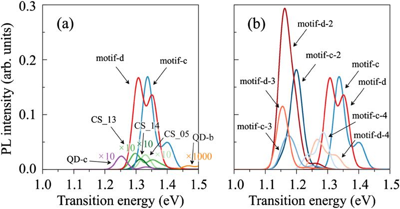
New J. Phys. 22 (2020) 093037                                                                                        Z-M Ji et al

is the antisymmetrizing operator):

                                                                Nv
                                                                   Nc
                                                  Ψ(γ) =                       (γ)
                                                                              Cv,c Φv,c ,                                   (3)
                                                                v =1 c =1

where N c and N v (N = N c + N v ) are the numbers of electron and hole states included in the expansion of
Ψ(γ) , respectively. The coefficients Cv,c
                                      (γ)
                                          are the eigenstates of the CI Hamiltonian:


                                              Nv
                                                 Nc
                                                                          (γ)       (γ)
                                                              Ĥvc,v c Cv,c = Eγ Cv,c .                                   (4)
                                              v  =1 c  =1

The CI matrix elements are expressed as:

                     Ĥvc,vc = Φv,c Ĥ  Φv,c = (εc − εv ) δv,vδc,c − Jvc,vc + Kvc,vc ,                          (5)

herein Jvc,v c are the Coulomb integrals and Kvc,v c are the exchange integrals. The exciton transition energy
E0 is defined as the difference in the total energy of a QD in a dominant configuration of an electron in level
e0 and a hole in level h0 and a QD in the ground state [53]:

                                                  E0 = E1,1 e10 , h10 − E0,0 ,                                              (6)

where E1,1 (e10 , h10 ) = εe0 − εh0 − Je0 h0 ,e0 h0 + Ke0 h0 ,e0 h0 , εe0 and εh0 are the single-particle energy level of lowest
unoccupied state (i.e., CBM) and highest occupied state (i.e., VBM), respectively. By directly diagonalizing
                                                                                          (γ)
the CI Hamiltonian, we are ready to get the excitonic eigenvalues Cv,c                        and then the many-body optical
transition dipole matrix elements [49],

                                                      (γ)
                                                    Mcv   =             (γ)
                                                                      Cc,v  ψc |r̂|ψv  ,                                   (7)
                                                                c,v

here r̂ is the position operator and ψc |r̂|ψv  is the single-particle transition matrix element.
    The QD emission spectrum is calculated from Fermi’s golden rule occupying the lowest energy initial
states according to the Boltzmann distribution at temperature T [54, 55]:
                                                                       E −E
                                                                      −( γk T 0 ) −( E−Eγ )2
                                                                  γ fγ e         e λ
                                                                           B
                                           I (E, T) =                         E −E            ,                            (8)
                                                                             −( γk T 0 )
                                                                           γe
                                                                                  B


                   (γ) 2
                 2Mcv
wherein fγ = mEγ is the oscillator strength which is unitless, λ is the Gaussian broadening, and kB the
Boltzmann’s constant. At thermal equilibrium under temperature T, photoexcited exciton occupies the
exciton states unequally according to the Boltzmann distribution; the probability of an excitonic state of
energy Eγ relative to the probability of the ground exciton state of energy E0 is determined by the
Boltzmann’s factor exp − Eγ − E0 /kB T . In the actual, the spectral line type should be the so-called
Voigt profile, which is the convoluted form of either Gaussian broadening due to its own oscillations and
Lorentz broadening due to natural lifespan and particle collision [56]. The broadening is temperature
dependent as a result of phonon scattering and impacted by size distribution in a QD ensemble. In this
work, for simplicity, we fix the spectral line to a Gaussian type with a broadening parameter of λ = 20 meV
as usual [30, 57, 58].

3. Results and discussions

3.1. Size-dependent scaling law of optical bandgap of Si and Ge QDs
Before going to identify the real mechanism underlying the light emission from Si and Ge QDs, it is
necessary to examine the variation of the bandgap as a function of dot size, which is one of the most
famous scaling laws of semiconductor QDs [9, 35, 59, 60]. Emission photon energy is higher when
electron–hole pairs are confined to a smaller volume [59, 60]. Many factors contribute to the precise scaling
of bandgap versus QD size, including variations of the quantum-confinement-induced shift in electron and
hole energy levels, intervalley and interband coupling, tunneling of electrons and holes through finite
confinement barriers, and the Coulomb and exchange interactions between electron and hole [61]. These
factors come into play in deciding the PL energy as well as light emission of a size tuning series of QDs
[30, 31, 62]. Figure 2 presents the calculated optical bandgap as a function of dot diameter for both Si and
Ge QDs, in comparison with the results obtained using the effective mass approximation (EMA) [60] and

                                                     4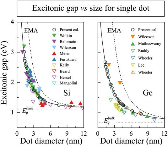
New J. Phys. 22 (2020) 093037                                                                                               Z-M Ji et al

   Figure 2. Atomistic pseudopotential method calculated excitonic gap (or optical gap) against dot diameter D for (a) single pure
   Si QDs and (b) single pure Ge QDs, in comparison with the corresponding experimental values. We use regular triangles for
   optical bandgap deduced from optical absorption data [4, 63, 71, 73], and inverted triangles for PL data [18, 63, 65–71, 73]. We
   also use solid triangles to indicate hydrogen passivated QDs, hollow triangles for QDs passivated by alkyl ligand, and striped
   triangles for passivated by OAM/ODE ligand. The dotted lines are the bandgap of the bulk materials, the dashed lines are the
   bandgap sizing curves calculated by the EMA model [60], and the solid lines are the fitting curves of our calculation results.
   Experimental data are taken from references [4, 18, 63–68] for Si QDs and references [69–74] for Ge QDs.

experimental data from various samples and groups [4, 18, 63–74]. Note that such a comparison has been
repeatedly conducted out in considerable literature (for example, references [9, 30, 35, 59, 73]). However,
the fundamental purpose here is to illustrate the reliability of the adopted semi-empirical pseudopotential
method, which has been extensity used for a wide variety of semiconductors nanostructures [55], for
prediction of optical properties of both Si and Ge QDs. Remarkably, in Ge QDs, besides the easily
size-tunable red-NIR emission with microsecond to millisecond scale, the more frequently observed
UV-green PL with nanosecond scale is less size-dependent [32, 35]. Such size-independent PL band has
been well explained as the recombination of surface state electron with QD core hole or the directly
radiative recombination of electron–hole pairs bonded on the surface [17, 18, 35, 36].
    Our primary motivation in this work purpose here is to reveal the light emission from the QD core.
Therefore, we chose the experimental data with reasonable size-dependent PL energy to avoid data
associated with surface defects. From the bandgap-size relationship shown in figure 2, we can see that the
effective mass model has a comparatively accurate description of the bandgap at larger QD sizes, but is
significantly overestimated at smaller QD size. In striking contrast, our predicted optical gaps based on the
semi-empirical pseudopotential method are consistent with the experimental results in the whole range of
dot diameter D. The fitting curves of the calculation results are carried out according to the following
expression proposed by Allen and Delerue [76]:

                                                                           1
                                              EgQD (D) = Egbulk −                  .                                                  (9)
                                                                      aD2 + bD + c

For Si QDs, Egbulk = 1.12 eV, a = 0.109, b = 0.158, and c = 0.159; and for Ge QDs, Egbulk = 0.67 eV,
a = 0.039, b = 0.153, and c = 0.223. These good agreements establish that the atomistic pseudopotential
method is a suitable choice for studying light emission from Si and Ge QDs.
    Although the size scaling law has attracted much attention, the absolute QD size is not an appropriate
parameter in the comparison of optical properties between Si and Ge QDs. For instance, as we mentioned
in the introduction section, with the decrease of the size of indirect bandgap QD, the
space-confinement-induced spread of the electron/hole wave functions in k-space increases, making the
zero-phonon vertical transition more possible [19]. This phenomenon is more pronounced when the
particle size is smaller than the exciton Bohr radius of the bulk counterpart as the quantum confinement
effect emerges. Nonetheless, the Bohr radius of Ge (∼11.5–24 nm) is much bigger than that of
Si (∼4.5 nm) [35]. Therefore, for Si and Ge QDs of the same size, the quantum confinement effect should
be more significant in the latter. This expectation of energy is clearly illustrated in the sizing curve in
figure 2. Bear this in mind: we will use the confinement energy ΔE = EgQD − Egbulk rather than the
commonly used dot size as the measuring parameter for quantum confinement effect in different QDs.

                                                      5
New J. Phys. 22 (2020) 093037                                                                                                 Z-M Ji et al

   Figure 3. Calculated optical properties of Si and Ge QDs with comparable quantum confinement energy. (Top) emission spectra
   at room temperature. The green profile represents the spectral line with a Gaussian broadening of 20 meV, and the orange
   vertical lines denote that without broadening. (middle) the absorption spectra without widening (black vertical lines) and the
   probability of an exciton state being thermally excited (red curve). The black dashed line marks the position of the first excitonic
   energy. (bottom) single-particle momentum matrix element of the transitions between the near band edge states (electron to
   hole).

3.2. Light emission from Si and Ge QDs
In bulk Si and Ge, zero-phonon radiative transitions are forbidden because both materials are indirect
bandgap semiconductors [16]. As we discussed in the introduction section, no-phonon emission becomes
possible in their nanocrystal counterparts [1–8]. In this case, the optical properties of Si and Ge QDs
depend on the result of the competition between zero-phonon quasi-direct recombination and
phonon-associated indirect recombination channels [9, 16]. Particularly, in Si QDs, the radiative transitions
transform from being governed by phonon-associated indirect recombination to be dominated by
no-phonon quasi-direct processes when confinement energy above 0.7 eV [20]. As we are interested in the
mechanism underlying the quantum-confinement-enhanced light emission from Si and Ge QDs, we
consider only the zero-phonon radiative recombination with neglecting the phonon-related recombination.
    Figure 3 compares the calculated zero-phonon emission spectra of Si and Ge QDs with confinement
energy slightly larger than 0.6 eV at room temperature. From the figure, one can see that two Si QDs with
the same shape and lattice symmetry but tiny size difference have a considerable disparity in PL intensity
(named as ‘QD-a’ for the one with stronger in PL and ‘QD-b’ for the one with weaker in PL). Moreover, the
PL intensity of the Ge QD (designated as ‘QD-c’) is not stronger than that of QD-a. Regarding the
intervalley coupling mechanism, the no-phonon transition intensity is inversely proportional to the square
of the energy separation between direct and indirect bandgap of the bulk material [16]. Such an energy
difference in bulk Ge is one order of magnitude smaller than that in bulk Si (0.14 vs 2.38 eV) [34].
Therefore, we may speculate that the space confinement mechanism is dominant over the intervalley
coupling mechanism in no-phonon light emission from indirect bandgap QDs. Besides, we can see multiple
peaks in the no-phonon PL spectra of both Si and Ge QDs at room temperature. Particularly in the Ge QD
(QD-c), PL has two main peaks. Although the lower one has a much larger thermal occupation than the
higher one, the latter even has a greater intensity than the former.

                                                       6
New J. Phys. 22 (2020) 093037 Z-M Ji et al
Table 1. Possible symmetry of the excitons (capital letters) formed
from the CBM and VBM (lower case letters) of Si and Ge QDs with
of T d symmetry in the single group notation by neglecting the
spin–orbit coupling. The asterisk represents the exciton state being a
‘bright’ state.
CBM
Exciton manifold
a1 e t2
t1 T1 T1+ T2∗ T 1 + T 2 ∗ + E + A2
VBM
t2 T2∗ T1+ T2∗ T 1 + T 2 ∗ + E + A1
According to the emission spectrum expression equation (8), the peak luminous intensity depends
mainly on the oscillator strength fγ of the corresponding energy states and the probability of these states
being thermal accessed. As can be seen from the absorption spectra in figure 3, the apparent distinction
(one order of magnitude) in PL intensity between two Si QDs of pretty close size about 3 nm in diameter
must chiefly arise from the significant difference in the oscillator strength of the low energy transition. As
(γ) 2
we know, the transition matrix element Mcv is the primary determinant of oscillator strength [16, 77]. In
the framework of CI, the many-body transition matrix element is a linear combination of the single-particle
transition matrix elements (See reference [49], and equation (7)). The lowest-energy many-body transitions
are usually composed of the single-particle transitions between CBM and VBM.
For Si and Ge QDs with the symmetry of the T d point group, the VBM is threefold degenerate (without
regard to spin–orbit coupling, otherwise splits into twofold and non-degenerate states [61]) with t 2
symmetry and occasionally with t 1 symmetry. Whereas the CBM could be an a1 , e, or t 2 state derived from
six equivalent bulk X-valleys for Si QDs, or an a1 or t 2 state derived from four equivalent bulk L-valleys for
Ge QDs, depending on the QD size [28, 29, 31, 62, 78]. The resulting manifold of excitonic states is
obtained in light of the multiplication table of the T d point group (e.g., t2 ⊗ a1 = T2 , t2 ⊗ e = T1 ⊕ T2 ,
t2 ⊗ t2 = A1 ⊕ E ⊕ T1 ⊕ T2 , and more details see table 1) [31, 62]. Since the electric dipole transition
operator er̂ possesses T2 symmetry, only the T2 exciton is optically active or ‘bright’, and remaining excitons
are optically passive or ‘dark’ [16]. The electron–hole exchange interaction will further split the bright
exciton T2 into a lower-energy spin-forbidden ‘dark’ triplet and a higher-energy spin-allowed ‘bright’
singlet [31, 62]. Many experiments evidence an anomalous lengthening of the decay times at low
temperatures, attributed to such exchange-interaction-induced dark–bright splitting, which are greatly
enhanced by quantum confinement [33, 79]. In our previous work, we have illustrated that in the direct gap
QDs (such as InAs QDs), the electron–hole exchange interaction is dominated by the long-range
component. In contrast, in the indirect gap QDs (such as Si QDs), only the short-range component
survives. Consequently, the exciton dark/bright splitting scales as ∼D−2 in InAs dots and ∼D−3 (enlarge
from 2 meV to 12 meV as dot size reduced from 4 nm to 2 nm) in Si dots [50].
Considering that the exchange-induced dark/bright splitting has a good relationship with dot size, it is
unlikely to have a dramatic difference in the dark/bright splittings between two spherical QDs (made by the
same material) with a similar size. In the case of two size-comparable Si QDs, as shown in figure 3, the large
scatter in their PL intensity is mainly because of their substantial difference in the oscillator strength of the
transitions between CBM and VBM. Since the CBM of both dots is a1 state and VBM is t 2 state, the
potential change of energy ordering of X-derived states does not occur here. Regarding the
space-confinement-induced PL intensity depends only on dot size, the remarkable disparity between the
oscillator strength of these two Si QDs with very similar size must be attributed to the effect of the
intervalley coupling mechanism. More frankly, the surface potential between the two Si QDs may be
different in atomic scale although they are both cut out using spheres with a tiny change in radius. In QD-b,
the intervalley coupling mechanism cancels the contribution of the space confinement mechanism partially.
To disentangle the contributions from the space confinement mechanism and intervalley coupling
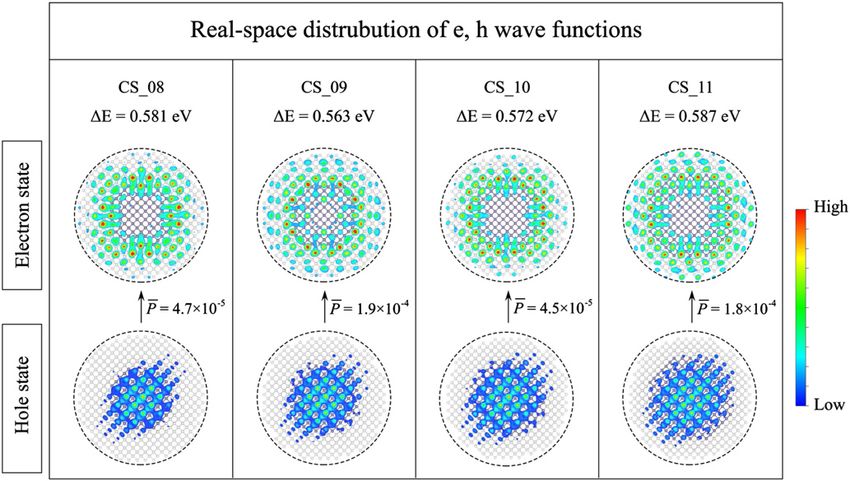
mechanism to light emission, we have compiled a size series of spherical Si and Ge QDs. Figure 4(a) gathers
the calculated PL intensity as a function of confinement energy in the range of 0–1.1 eV. This trend closely
resembles that of the oscillator strength against quantum confinement energy in figure 4(b). The strong
dependence of the oscillator strength on size and shape yields the large scatter, but a robust overall trend.
This scatter has also been found in previous calculations of Si QDs [19, 28]. Besides the intervalley coupling
induced remarkable change in oscillator strength, the change of energy ordering among the band edge states
[28, 31] will influence the thermal occupation of bright states, as shown in figure 4(c), which may also yield
fluctuation in PL intensity as varying dot size or shape. Both Si and Ge QDs sharing the same overall trend
is in sharp contrast to the expectation of much stronger light emission occurred in Ge QDs relative to Si
QDs according to the intervalley coupling mechanism. It thus rules out the mechanism of
7New J. Phys. 22 (2020) 093037 Z-M Ji et al
Figure 4. (a) The calculated emission intensity, (b) the sum of the oscillator strengths of the transitions corresponding to the
emission peak, (c) the thermal occupation probability of these excitonic states, (d) the Γ -component of conduction states that
genuinely contribute to the luminescence at room temperature as a function of quantum confinement energy for spherical Si and
Ge QDs, in comparison with the results of Ge/Si core/shell QDs as well as Ge/Si core/multishell QDs. Orange diamond: Si QD,
violet square: Ge QD, green point: Ge/Si core/shell QD, and red hexagonal: Ge/Si core/multishell QD. The solid line is the result
of a linear fitting of data from Si and Ge QDs. The QDs we focus on are marked.
interface-scattering-induced intervalley coupling as the primary factor for breaking the momentum
conservation rule in Si and Ge QDs. Therefore, we have demonstrated unambiguously that the space
confinement mechanism dominates the light emission from indirect bandgap QDs.
3.3. Enhanced light emission from Ge/Si core/shell QDs
Figure 4(a) shows that some scatter points deviate from the overall trend of PL intensity, which should arise
from the effect of surface-potential-induced intervalley coupling. These scatter points imply that one may
engineer the crystal potential to enhance the light emission of Si or Ge QDs significantly. For instance,
Dohnalová et al [25] have demonstrated that replacing the oxygen or hydrogen surface termination by
carbon surface termination can enhance the radiative rate of Si QDs by about two orders of magnitude.
Moreover, Miyazaki et al [39, 40] have also presented encouraging results in their experiments that cladding
Ge QD with Si shell can improve the luminescence efficiency, despite the type-II band alignment (spatial
separation of electrons and holes in the Si shell and Ge core, respectively) generally results in reduced
emission intensity [80, 81]. Miyazaki et al argued that the suppression of non-radiative recombination in
Ge/Si core/shell QDs is the principal reason for the luminescence enhancement [39, 40]. An alternative
explanation came up that the improved localization of electron and hole carriers in the Ge core is
responsible for enhanced luminescence in Ge/Si core/shell QDs [39, 40, 82, 83]. But in our view, this
argument does not hold water.
Figure 4(a) also presents the calculated emission intensity of Ge/Si core/shell QDs with total QD radius
fixed to 16 monolayers (MLs) but varying the Si shell from 11 ML to 1 ML in a step of 1 ML
(correspondingly, the Ge core radius increased from 5 ML to 15 ML). We name these 11 core/shell QDs as
CS_05–CS_15, where CS is the abbreviation of ‘core/shell’ and the number is for Ge core radius units in
ML. The confinement energy of the Ge/Si core/shell QDs is defined as the energy difference between the
QD optical gap and Ge bulk bandgap. Here, we take the bulk Ge as the reference regarding the quantum
confinement of Ge/Si core/shell QDs comes mostly from holes. The holes are highly confined in the Ge core
region by the 0.5 eV valence-band offset between Si and Ge, while the electrons are rather delocalized with a
slightly larger component in the Si region because of the small conduction-band offset (∼5 meV). One can
see from figure 4(a) that the calculated emission intensity changes by order of magnitude as varying Si shell
8New J. Phys. 22 (2020) 093037 Z-M Ji et al
Figure 5. The real-space charge density of energy states with the principal contribution to the most potent transitions in four
different core/shell QDs CS_08, CS_09, CS_10, and CS_11 with comparable diameter but different shell thickness. The
cross-section contours are plotted on the [001] atomic plane, with the intensity increasing from blue to red. The boundary of
quantum dots (QDs) is outlined with black dashed rings. Silicon and germanium atoms are represented by white and grey
spheres, respectively. It also includes the moment transition matrix element between the electron state and the hole state in the
figure.
thickness. Because the surface defects are absent in all calculated QDs, the enhanced emission intensity of
Ge/Si core/shell QDs is not merely attributed to the suppression of non-radiative recombination, as
suggested by Miyazaki et al [39, 40]. Meanwhile, Miyazaki et al [39, 40] also deemed that the localization of
holes may lead to the enhancement of luminescence. But the nonmonotonic dependence of emission
intensity on Si shell thickness further proves that this view is unreasonable. Figure 5 displays the wave
function distributions of electron and hole of four selected Ge/Si core/shell QDs. We find that their small
variation in wave function distributions is hard to yield several-fold differences in moment transition
matrix element among the investigated Ge/Si core/shell QDs.
So far, we have demonstrated that there are two factors raised the variation in luminescence intensity
around the strong overall trend: (i) the oscillator strength and (ii) the thermal occupation of the bright
excitons, as shown in figures 4(b) and (c), respectively.
The oscillator strength is proportional to the overlap of wave functions of electron and hole in k-space.
Given that the hole is most spread around the Γ -point in bulk BZ, we can analyze the oscillator strength by
accessing the component of the QD electron state around the Γ -point. In doing so, we can project QD’s
electron state ψi (r) into the Bloch states ϕn,k (r) of the underlying bulk crystal, say Si or Ge [24]:
∞
1 k N
ψi (r) = √ ci,n (k) · ϕn,k (r) , (10)
N n k
here ϕn,k (r) = exp(ik · r)un,k(r), k and n are bulk wave vector and band index in the bulk BZ, respectively,
and ci,n (k) is the expansion coefficient for QD energy level i. Consequently, the single-particle momentum
matrix element in QDs is [24]:
∞ ∞
1 k k N N
∗
Pc,v = ψc |p̂|ψv = cc,n c
(kc ) · cv,nv (kv ) · Pnc ,nv · δkc ,kv , (11)
N n n
c v kc kv
where Pnc ,nv = unc ,kc (r)|p̂|unv ,kv (r) is the momentum matrix element of the bulk Bloch wave functions. A
relationship between the momentum matrix element and the dipole matrix element is [75]
ψc |p̂|ψv = imωvc ψc |r̂|ψv . (12)
ωvc is the single-particle transition energy. According to equation (11), the quantum confinement effect
causes a finite overlap between cc,nc (kc ) and cv,nv (kv ), as depicted in figure 1(a). This finite overlap is
responsible for the quantum confinement effect induced breaking of the momentum conservation law δkc ,kv ,
and making the zero-phonon transition possible. Since the holes are mostly spread around the Γ -point, the
9New J. Phys. 22 (2020) 093037 Z-M Ji et al
zero-phonon Γ –Γ transition depends heavily on the Γ -component in the QD electron states. To quantify
the weight of each bulk Bloch wave function mixed into the QD electron states, we use the ‘majority
representation’ approach [84] with the projection technique:
pi (k) = |ψi (r)|ϕn,k (r)|2 (13)
n
Besides, we employ a more intuitive weight function ωiΓ (X,L) for estimating band mixing, by summing pi (k)
of all k points in a spherical region centered on Γ (X, L) points [85]:
ωiΓ (X,L) = pi (k) , (14)
k∈ΩΓ (X,L)
where the radii of the spheres ΩΓ , ΩX and ΩL are identical.
Figure 4(d) depicts the Γ -component of the conduction band states (usually the CBM) that dominate
the light-emitting for Ge/Si core/shell QDs as well as Si and Ge QDs. The overall trend of the Γ -component
data points against the confinement energy for all investigated QDs is closely following the oscillator
strength. This good agreement indicates a strong correlation between light emission and Γ -component of
electronic states. Hence, we can attribute the enhancement of light emission in Ge/Si core/shell QDs to the
increase in the Γ -component of band edge electron states. There is no need to invoke the real-space
distribution of wave functions, and the suppression of nonradiative recombination associated with surface
defects for the observed stronger light emission from Ge/Si core/shell QDs [39, 40].
We also note in figure 4 that, compared with the emission intensity, the oscillator strength and the
Γ -component of electron states of Ge/Si core/shell QDs are more significant above the overall trend of Si
and Ge QDs. This is because the transitions corresponding to the strongest PL peak in core/shell structures
are often from the higher energy electron state with a smaller thermal occupation rather than CBM. The
unsurprisingly reduced thermal occupation is presented in figure 4(c). For Si and Ge QDs, the data points
are less scattered in Γ -component than those in the emission intensity. Specifically, the above discussed two
Si QDs (QD-a and QD-b) have one order of magnitude difference in both emission intensity and oscillator
strength but have similar Γ -component, implying the sum over Γ -point does not precisely reflect the detail
overlap between electron and hole wave functions. The Γ -component data of QD-c is well above the overall
trend, which is twice as large as that of QD-a, as shown in figure 4(d). However, the reduced thermal
occupation renders it has a comparable light emission as the latter. These findings imply we can further
enhance light emission via enhancing both the thermal occupation and CBM Γ -component.
3.4. Enhance light emission via interface-engineering in Ge/SiGe core/multishell QDs
In previous works, we have designed direct bandgap Si/Ge superlattices [58] and core/multishell nanowires
[57] with substantially enhanced light absorption using a genetic algorithm inverse band structure
approach. Here, we simply take Si/Ge motifs responsible for the enhanced light absorption from
superlattices and nanowires into the Ge/SiGe core/multishell QDs without conducting additional inverse
design, which demands much more computationally cost for QDs. Specifically, we take
[Si1 Ge2 Si2 Ge2 Si1 Gej ] motif (motif-a) from direct bandgap Si/Ge superlattices [58], [Ge1 Si2 Ge1 Si2 Gej ] motif
(motif-b) from inverse designed [100] oriented Ge/SiGe core/multishell nanowires, and [Si1 Ge3 Si2 Gej ]
(motif-c) and [Ge4 Si2 Gej ] (motif-d) motifs from [110] oriented Ge/SiGe core/multishell nanowires [57].
First, we attach these four motifs to a Ge core with a size of 5 ML from the center atom to the interface, and
varying j in each motif to ensure 16 ML in total from the central atom to the outermost surface atom (the
configuration space is illustrated in figure 6(a)). It will produce four Ge/SiGe core/multishell QDs (motif-a
is shown as an example in figure 6(b)). We compare the light emission of these four core/multishell QDs
with Si, Ge, and Ge/Si core/shell QDs in figure 4(a). Interestingly, motif-c and motif-d core/multishell QDs
exhibit one order of magnitude enhancement in light emission relative to the Ge/Si core/shell QDs with the
strongest luminescence. Whereas, motif-a and motif-b core/multishell QDs have comparable light emission
with Ge/Si core/shell QDs.
As seen in figure 4, motif-c and motif-d with the strongest luminescence among the four core/multishell
QDs have not only strong oscillator strength but also high thermal occupancy. The QD (motif-b) with the
medium PL intensity possesses nearly the same thermal occupation probability as motif-c and motif-d.
However, the oscillator strength is less than one-tenth of the latter two. As for the QD (motif-a) with the
weakest luminescence, the thermal occupation probability is far less than that of motif-b, although their
oscillator strengths are comparable. The comparison of the two factors, oscillator strength and thermal
occupation, explains the light emission behavior of core/multishell QDs well, which is in line with our
previous argument.
10New J. Phys. 22 (2020) 093037 Z-M Ji et al
Figure 6. (a) Schematic diagram of the configuration space of Ge/SiGe core/multishell QDs. (b) Cross-section of atom structure
through the QD center for Ge/SiGe core/multishell QD with a motif-a. Grey and white spheres, respectively represent
germanium and silicon atoms. (c) The reciprocal-space projection of electron state and hole state that dominate the
luminescence into the bulk fcc BZ for motif-a and motif-c. The inset zooms in the k-space distribution of electronic states
around the Γ -point, and numbers label the bulk Γ -component in percentage. The partially-preserved symmetry of the states is
presented. Here we also give the corresponding moment matrix element P (unit in a.u.).
Nevertheless, we find in figure 4(d) that there is little variance in the Γ -component of the four
core/multishell QDs, which cannot explain one order of magnitude differences in their oscillator strength.
In the last paragraph of the previous section, we have pointed out that the Γ -component may fail to reflect
the k-space distribution of the wave function accurately. In this paragraph, we will take core/multishell QDs
motif-a and motif-c as examples to clarify this contradiction. Among the four core/multishell QDs, motif-a
and motif-c have the closest quantum confinement energies, and the Γ -components of the electron states
that dominate their respective light-emitting are nearly the same, while the corresponding oscillator
strengths differ by more than one order of magnitude. Figure 6(c) exhibits a detailed comparison of the
k-space wave functions of the electron states and hole states that are top contributors to the luminescence of
motif-a and motif-c. One can find a stark contrast between the k-space wave functions of the two electronic
states from the figure. In particular, the k-space wave function of motif-a displays a minor component with
a uniform distribution around the Γ -point. Whereas, the k-space wave function of motif-c has a local
maximum (with more substantial component) around the Γ -point, evidencing the effect of the intervalley
coupling mechanism. In the computation of Γ -component, we may use too large integration radius Ω, so
that a part of Bloch components in Γ -component do not give rise to no-phonon vertical transition with the
hole. Subsequently, motif-a has a slightly larger Γ -component but one order of magnitude weaker in
oscillator strength than motif-d. The same argument can also explain that the oscillator strengths in some
core/shell QDs are less than one tenth of those in motif-c or motif-d, regardless of the advantage of the
former in the Γ -component of the electronic state.
To access the robust of motif-c and motif-d for intense light emission, we increase the Ge core radius
from 5 ML to 10 ML for motif-c and motif-d core/multishell QDs (labeled as motif-c-2 and motif-d-2). We
also add six Ge MLs to the outermost of motif-c and motif-d core/multishell QDs (labeled as motif-c-3 and
11New J. Phys. 22 (2020) 093037 Z-M Ji et al
Figure 7. Comparison of the simulated room-temperature emission spectra of core/multishell QDs motif-c and motif-d with
(a) Si, Ge, Ge/Si core/shell QDs whose quantum confinement energy close to them; (b) core/multishell QDs derived from each of
them. The spectral line is a Gauss type with a broadening of 20 meV. Too weak lines are amplified to be seen.
motif-d-3). Finally, we alternatively change the outermost six Ge MLs to two Si MLs (labeled as motif-c-4
and motif-d-4). Figure 7 depicts the calculated emission spectra of these modified QDs. Interestingly, we
find a further enhancement in light emission from motif-c-2 and motif-d-2 core/multishell QDs. In other
cases, the luminescence is reduced about three times but is still hundreds of times stronger than that of
corresponding Ge QDs. In this way, we have shown explicitly that based on the valley coupling mechanism,
the light emission can be significantly improved through interface engineering.
4. Conclusion
By performing atomistic semiempirical pseudopotential calculations, in this work, we attempt to unravel
the hierarchical relationship between two primary mechanisms proposed to explain the light emission in
both Si and Ge indirect bandgap QDs. We find that in both Si and Ge QDs, the space confinement
mechanism originating from the Heisenberg uncertainty principle dominates the zero-phonon light
emission. While the surface-potential-induced intervalley coupling mechanism plays a minor role, which
causes scattering of QDs away from the strong overall trend of light emission intensity against the
confinement energy. This implies that one may engineer the surface potential to enhance the light emission
of Si or Ge QDs significantly. In Ge/Si core/shell QDs we discover that the emission intensity could indeed
change by one order of magnitude as varying Si shell thickness. Because the surface defects are absent in all
calculated QDs, and the emission intensity does not monotonically change with the Si shell thickness, the
enhanced emission intensity in Ge/Si core/shell QDs is due to neither the suppression of non-radiative
recombination nor the severe localization of holes, which are suggested by Miyazaki et al [39, 40]. We
further engineer the Ge QD interface by bringing four motifs of Si/Ge multiple layers, which were designed
to have intense light absorption for superlattices or nanowires. We find two out of four motifs always give
rise to two orders of magnitude enhancement in light emission relative to the Ge and Si QDs. So far, we
study ideal Si and Ge QDs in spherical shapes. Note that complex structures on QDs’ surfaces are reported
in voluminous literature [86–89]. For instance, in our previous work [89], we have found that the surface of
Si QDs embedded in an oxide matrix can contain numerous interface defects, which will strongly affect the
QD PL efficiency and optical absorption. It indicates one may further enhance the light emission from Ge
and Si QDs via surface engineering by considering these complex surface factors. Our findings shed new
light on light emission from Si and Ge QDs and undoubtedly give good prospects to realize high-efficiency
Si-based light sources.
Acknowledgments
This work was supported by the National Key Research and Development Program of China under Grant
No. 2018YFB2200105, Key Research Program of Frontier Sciences, CAS under Grant No. ZDBS-LY-JSC019,
and the National Natural Science Foundation of China (NSFC) under Grant No. 61811530022.
12New J. Phys. 22 (2020) 093037 Z-M Ji et al
ORCID iDs
Zhi-Min Ji https://orcid.org/0000-0001-5446-0748
Jun-Wei Luo https://orcid.org/0000-0002-1147-8267
References
[1] Cullis A G and Canham L T 1991 Visible light emission due to quantum size effects in highly porous crystalline silicon Nature 353
335–8
[2] Canham L T 1990 Silicon quantum wire array fabrication by electrochemical and chemical dissolution of wafers Appl. Phys. Lett.
57 1046–8
[3] Lehmann V and Gösele U 1991 Porous silicon formation: a quantum wire effect Appl. Phys. Lett. 58 856–8
[4] Furukawa S and Miyasato T 1988 Quantum size effects on the optical band gap of microcrystalline Si:H Phys. Rev. B 38 5726
[5] Takagi H, Ogawa H, Yamazaki Y, Ishizaki A and Nakagiri T 1990 Quantum size effects on photoluminescence in ultrafine Si
particles Appl. Phys. Lett. 56 2379–80
[6] Kim T-Y, Park N-M, Kim K-H, Sung G Y, Ok Y-W, Seong T-Y and Choi C-J 2004 Quantum confinement effect of silicon
nanocrystals in situ grown in silicon nitride films Appl. Phys. Lett. 85 5355–7
[7] Holmes J D, Ziegler K J, Doty R C, Pell L E, Johnston K P and Korgel B A 2001 Highly luminescent silicon nanocrystals with
discrete optical transitions J. Am. Chem. Soc. 123 3743–8
[8] Rosso-Vasic M, Spruijt E, van Lagen B, De Cola L and Zuilhof H 2008 Alkyl-functionalized oxide-free silicon nanoparticles:
synthesis and optical properties Small 4 1835–41
[9] Belyakov V A, Burdov V A, Lockwood R and Meldrum A 2008 Silicon nanocrystals: fundamental theory and implications for
stimulated emission Adv. Opt. Technol. 2008 1–32
[10] Iyer S S and Xie Y-H 1993 Light emission from silicon Science 260 40–6
[11] Baehr-Jones T, Pinguet T, Lo Guo-Qiang P, Danziger S, Prather D and Hochberg M 2012 Myths and rumours of silicon
photonics Nat. Photon. 6 206–8
[12] Asghari M and Krishnamoorthy A V 2011 Energy-efficient communication Nat. Photon. 5 268–70
[13] Hirschman K D, Tsybeskov L, Duttagupta S P and Fauchet P M 1996 Silicon-based visible light-emitting devices integrated into
microelectronic circuits Nature 384 338–41
[14] Ng W L, Lourenco M A, Gwilliam R M, Ledain S, Shao G and Homewood K P 2001 An efficient room-temperature silicon-based
light-emitting diode Nature 410 192–4
[15] Green M A, Zhao J, Wang A, Reece P J and Gal M 2001 Efficient silicon light-emitting diodes Nature 412 805–8
[16] Peter Y U and Cardona M 2010 Fundamentals of Semiconductors: Physics and Materials Properties (Berlin: Springer)
[17] Godefroo S, Hayne M, Jivanescu M, Stesmans A, Zacharias M, Lebedev O I, Van Tendeloo G and Moshchalkov V V 2008
Classification and control of the origin of photoluminescence from Si nanocrystals Nat. Nanotechnol. 3 174
[18] Wolkin M V, Jorne J, Fauchet P M, Allan G and Delerue C 1999 Electronic states and luminescence in porous silicon quantum
dots: the role of oxygen Phys. Rev. Lett. 82 197–200
[19] Hybertsen M S 1994 Absorption and emission of light in nanoscale silicon structures Phys. Rev. Lett. 72 1514
[20] Kovalev D, Heckler H, Ben-Chorin M, Polisski G, Schwartzkopff M and Koch F 1998 Breakdown of the k-conservation rule in Si
nanocrystals Phys. Rev. Lett. 81 2803
[21] Barbagiovanni E G et al 2014 Role of quantum confinement in luminescence efficiency of group IV nanostructures J. Appl. Phys.
115 044311
[22] De Boer W D A M, Timmerman D, Dohnalová K, Yassievich I N, Zhang H, Buma W J and Gregorkiewicz T 2010 Red spectral
shift and enhanced quantum efficiency in phonon-free photoluminescence from silicon nanocrystals Nat. Nanotechnol. 5 878
[23] Luo J-W, Li S-S, Sychugov I, Pevere F, Linnros J and Zunger A 2017 Absence of redshift in the direct bandgap of silicon
nanocrystals with reduced size Nat. Nanotechnol. 12 930
[24] Lee B G, Luo J-W, Neale N R, Beard M C, Hiller D, Zacharias M, Stradins P and Zunger A 2016 Quasi-direct optical transitions in
silicon nanocrystals with intensity exceeding the bulk Nano Lett. 16 1583–9
[25] Dohnalová K, Poddubny A N, Prokofiev A A, de Boer W D, Umesh C P, Paulusse J M, Zuilhof H and Gregorkiewicz T 2013
Surface brightens up Si quantum dots: direct bandgap-like size-tunable emission Light: Sci. Appl. 2 e47
[26] Pearsall T P, Vandenberg J M, Hull R and Bonar J M 1989 Structure and optical properties of strained Ge–Si superlattices grown
on (001) Ge Phys. Rev. Lett. 63 2104
[27] Hapala P, Kůsová K, Pelant I and Jelı́nek P 2013 Theoretical analysis of electronic band structure of 2- to 3-nm Si nanocrystals
Phys. Rev. B 87 195420
[28] Delley B and Steigmeier E F 1993 Quantum confinement in Si nanocrystals Phys. Rev. B 47 1397
[29] Ren S Y 1997 Quantum confinement of edge states in Si crystallites Phys. Rev. B 55 4665
[30] Luo J-W, Stradins P and Zunger A 2011 Matrix-embedded silicon quantum dots for photovoltaic applications: a theoretical study
of critical factors Energy Environ. Sci. 4 2546–57
[31] Reboredo F A, Franceschetti A and Zunger A 2000 Dark excitons due to direct Coulomb interactions in silicon quantum dots
Phys. Rev. B 61 13073
[32] Niquet Y M, Allan G, Delerue C and Lannoo M 2000 Quantum confinement in germanium nanocrystals Appl. Phys. Lett. 77
1182–4
[33] Robel I, Shabaev A, Lee D C, Schaller R D, Pietryga J M, Crooker S A, Efros A L and Klimov V I 2015 Temperature and
magnetic-field dependence of radiative decay in colloidal germanium quantum dots Nano Lett. 15 2685–92
[34] Madelung O 2012 Semiconductors: Data Handbook (Berlin: Springer)
[35] Carolan D 2017 Recent advances in germanium nanocrystals: synthesis, optical properties and applications Prog. Mater. Sci. 90
128–58
[36] Sykora M, Mangolini L, Schaller R D, Kortshagen U, Jurbergs D and Klimov V I 2008 Size-dependent intrinsic radiative decay
rates of silicon nanocrystals at large confinement energies Phys. Rev. Lett. 100 067401
[37] Sangghaleh F, Sychugov I, Yang Z, Veinot J G C and Linnros J 2015 Near-unity internal quantum efficiency of luminescent silicon
nanocrystals with ligand passivation ACS Nano 9 7097–104
13New J. Phys. 22 (2020) 093037 Z-M Ji et al
[38] Nestoklon M O, Poddubny A N, Voisin P and Dohnalova K 2016 Tuning optical properties of Ge nanocrystals by Si shell J. Phys.
Chem. C 120 18901–8
[39] Miyazaki S, Makihara K, Ohta A and Ikeda M 2016 Processing and characterization of Si/Ge quantum dots 2016 IEEE Int. Electron
Devices Meeting (IEDM) (Piscataway, NJ: IEEE) pp 33.2.1–4
[40] Makihara K, Ikeda M, Fujimura N, Yamada K, Ohta A and Miyazaki S 2017 Electroluminescence of superatom-like
Ge-core/Si-shell quantum dots by alternate field-effect-induced carrier injection Appl. Phys. Express 11 011305
[41] Hunter K I, Held J T, Mkhoyan K A and Kortshagen U R 2017 Nonthermal plasma synthesis of core/shell quantum dots: strained
Ge/Si nanocrystals ACS Appl. Mater. Interfaces 9 8263–70
[42] Nekić N et al 2019 Preparation of non-oxidized Ge quantum dot lattices in amorphous Al2 O3 , Si3 N4 and SiC matrices
Nanotechnology 30 335601
[43] Nekić N, Sancho-Parramon J, Bogdanović-Radović I, Grenzer J, Hübner R, Bernstorff S, Ivanda M and Buljan M 2017 Ge/Si
core/shell quantum dots in alumina: tuning the optical absorption by the core and shell size Nanophotonics 6 1055–62
[44] Claeys C and Simoen E 2011 Germanium-based Technologies: From Materials to Devices (Amsterdam: Elsevier)
[45] Hu Y Z, Zettler J T, Chongsawangvirod S, Wang Y Q and Irene E A 1992 Spectroscopic ellipsometric measurements of the
dielectric function of germanium dioxide films on crystal germanium Appl. Phys. Lett. 61 1098–100
[46] Millo O, Balberg I, Azulay D, Purkait T K, Swarnakar A K, Rivard E and Veinot J G C 2015 Direct evaluation of the quantum
confinement effect in single isolated Ge nanocrystals J. Phys. Chem. Lett. 6 3396–402
[47] Pryor C, Kim J, Wang L W, Williamson A J and Zunger A 1998 Comparison of two methods for describing the strain profiles in
quantum dots J. Appl. Phys. 83 2548–54
[48] Bernard J E and Zunger A 1991 Strain energy and stability of Si–Ge compounds, alloys, and superlattices Phys. Rev. B 44 1663
[49] Franceschetti A, Fu H, Wang L W and Zunger A 1999 Many-body pseudopotential theory of excitons in InP and CdSe quantum
dots Phys. Rev. B 60 1819
[50] Luo J-W, Franceschetti A and Zunger A 2009 Direct-bandgap InAs quantum-dots have long-range electron−hole exchange
whereas indirect gap Si dots have short-range exchange Nano Lett. 9 2648–53
[51] Wang L W and Zunger A 1994 Electronic structure pseudopotential calculations of large (approx. 1000 atoms) Si quantum dots J.
Phys. Chem. 98 2158–65
[52] Wang L W and Zunger A 1994 Solving Schrödinger’s equation around a desired energy: application to silicon quantum dots J.
Chem. Phys. 100 2394–7
[53] Shumway J, Franceschetti A and Zunger A 2001 Correlation versus mean-field contributions to excitons, multiexcitons, and
charging energies in semiconductor quantum dots Phys. Rev. B 63 155316
[54] Califano M and Zunger A 2004 Anisotropy of interband transitions in InAs quantum wires: an atomistic theory Phys. Rev. B 70
165317
[55] Bester G 2008 Electronic excitations in nanostructures: an empirical pseudopotential based approach J. Phys.: Condens. Matter. 21
023202
[56] Olivero J J and Longbothum R L 1977 Empirical fits to the Voigt line width: a brief review J. Quant. Spectrosc. Radiat. Transfer 17
233–6
[57] Zhang L, d’Avezac M, Luo J-W and Zunger A 2012 Genomic design of strong direct-gap optical transition in Si/Ge
core/multishell nanowires Nano Lett. 12 984–91
[58] d’Avezac M, Luo J W, Chanier T and Zunger A 2012 Genetic-algorithm discovery of a direct-gap and optically allowed
superstructure from indirect-gap Si and Ge semiconductors Phys. Rev. Lett. 108 027401
[59] Barbagiovanni E G, Lockwood D J, Simpson P J and Goncharova L V 2014 Quantum confinement in Si and Ge nanostructures:
theory and experiment Appl. Phys. Rev. 1 011302
[60] Takagahara T and Takeda K 1992 Theory of the quantum confinement effect on excitons in quantum dots of indirect-gap
materials Phys. Rev. B 46 15578
[61] Woggon U 1997 Optical Properties of Semiconductor Quantum Dots (Berlin: Springer)
[62] Reboredo F A and Zunger A 2001 Surface-passivation-induced optical changes in Ge quantum dots Phys. Rev. B 63 235314
[63] Wilcoxon J P, Samara G A and Provencio P N 1999 Optical and electronic properties of Si nanoclusters synthesized in inverse
micelles Phys. Rev. B 60 2704
[64] Meier C, Gondorf A, Lüttjohann S, Lorke A and Wiggers H 2007 Silicon nanoparticles: absorption, emission, and the nature of
the electronic bandgap J. Appl. Phys. 101 103112
[65] Hessel C M, Reid D, Panthani M G, Rasch M R, Goodfellow B W, Wei J, Fujii H, Akhavan V and Korgel B A 2012 Synthesis of
ligand-stabilized silicon nanocrystals with size-dependent photoluminescence spanning visible to near-infrared wavelengths
Chem. Mater. 24 393–401
[66] Kelly J A and Veinot J G C 2010 An investigation into near-UV hydrosilylation of freestanding silicon nanocrystals ACS Nano 4
4645–56
[67] Beard M C, Knutsen K P, Yu P, Luther J M, Song Q, Metzger W K, Ellingson R J and Nozik A J 2007 Multiple exciton generation
in colloidal silicon nanocrystals Nano Lett. 7 2506–12
[68] Mangolini L and Kortshagen U 2007 Plasma-assisted synthesis of silicon nanocrystal inks Adv. Mater. 19 2513–9
[69] Ruddy D A, Johnson J C, Smith E R and Neale N R 2010 Size and bandgap control in the solution-phase synthesis of
near-infrared-emitting germanium nanocrystals ACS Nano 4 7459–66
[70] Belomoin G, Therrien J, Smith A, Rao S, Twesten R, Chaieb S, Nayfeh M H, Wagner L and Mitas L 2002 Observation of a magic
discrete family of ultrabright Si nanoparticles Appl. Phys. Lett. 80 841–3
[71] Wilcoxon J P, Provencio P P and Samara G A 2001 Synthesis and optical properties of colloidal germanium nanocrystals Phys.
Rev. B 64 035417
[72] Muthuswamy E, Iskandar A S, Amador M M and Kauzlarich S M 2013 Facile synthesis of germanium nanoparticles with size
control: microwave versus conventional heating Chem. Mater. 25 1416–22
[73] Lee D C, Pietryga J M, Robel I, Werder D J, Schaller R D and Klimov V I 2009 Colloidal synthesis of infrared-emitting germanium
nanocrystals J. Am. Chem. Soc. 131 3436–7
[74] Wheeler L M, Levij L M and Kortshagen U R 2013 Tunable band gap emission and surface passivation of germanium nanocrystals
synthesized in the gas phase J. Phys. Chem. Lett. 4 3392–6
[75] Delerue C J and Lannoo M 2013 Nanostructures: Theory and Modeling (Berlin: Springer)
[76] Allan G and Delerue C 2004 Confinement effects in PbSe quantum wells and nanocrystals Phys. Rev. B 70 245321
[77] Hilborn R C 1982 Einstein coefficients, cross sections, f values, dipole moments, and all that Am. J. Phys. 50 982–6
14You can also read