Investor Presentation - March 2021 Atomera Incorporated
←
→
Page content transcription
If your browser does not render page correctly, please read the page content below
Investor Presentation
       March 2021

        Atomera Incorporated   1
Safe Harbor

      This presentation contains forward-looking statements concerning Atomera Incorporated (““Atomera,” the “Company,” “we,” “us,”
      and “our”). The words “believe,” “may,” “will,” “potentially,” “estimate,” “continue,” “anticipate,” “intend,” “could,” “would,” “project,”
      “plan,” “expect” and similar expressions that convey uncertainty of future events or outcomes are intended to identify forward-
      looking statements. These forward-looking statements are subject to a number of risks, uncertainties and assumptions, including
      those disclosed in the section "Risk Factors" included in our Annual Report on Form 10-K filed with the SEC on February 19,
      2021. In light of these risks, uncertainties and assumptions, the forward-looking events and circumstances discussed in this
      presentation may not occur and actual results could differ materially and adversely from those anticipated or implied in our
      forward-looking statements. You should not rely upon forward-looking statements as predictions of future events. Although we
      believe that the expectations reflected in our forward-looking statements are reasonable, we cannot guarantee that the future
      results, levels of activity, performance or events and circumstances described in the forward-looking statements will be achieved
      or occur.

      This presentation contains only basic information concerning Atomera. The Company’s filings with the Securities Exchange
      Commission, including the Prospectus Supplement , include more information about factors that could affect the Company’s
      operating and financial results. We assume no obligation to update information contained in this presentation. Although this
      presentation may remain available on the Company's website or elsewhere, its continued availability does not indicate that we are
      reaffirming or confirming any of the information contained herein.

                                                                  Atomera Incorporated                                                              2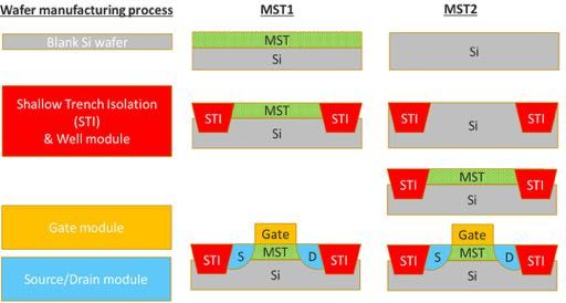
Investment Overview

  ► Mears   Silicon Technology (MST®) is a thin film used to enhance semiconductors
      § Results in higher performance, lower power, and lower costs for ICs

  ► Capital-light   IP and technology licensing business
      § Robust and growing patent portfolio

  ► Engaged    with 50% of world’s top semiconductor makers

  ► Licenses   with four companies including recent JDA

  ► Strong   team to commercialize technology

                                              Atomera Incorporated                    3
A Better Way for Industry R&D

                                                          In House R&D
  Industry Consortia   Equipment OEMs
                                                               Large Scale,   Targeted Innovation
     Little Control    No Longer Available                      Long Term
                                                                Investment       Inexpensive
     Expensive &            Tied to                                               & Low Risk
      Inefficient          Equipment
                             Sales

                                        Atomera Incorporated                                   4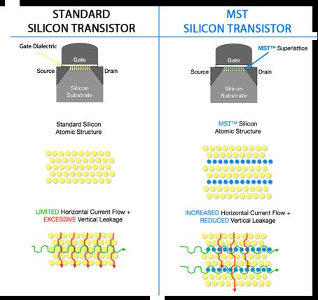
MST Technology

                                                     Potential Benefits

                                        ► Improved    Efficiency
                                           § Higher transistor performance
                                           § Lower power consumption
                                           § Better reliability

                                        ► Lower   cost
                                           § Reduced die size
                                           § Improved yield
                                           § Higher throughput

                                        ► Same   benefits as a node shrink

                 Atomera Incorporated                                        5
Patent Portfolio – 17% increase YoY

          269 Patents Granted and Pending                                        Discoverable
                                                                     These distinctive layers are visible on
                                                                             products using MST

      112
   US Patents

                  80                  59
                                    Foreign          21
                Pending
                                                     US
        75
      Foreign
      Patents

          Core MST Method and Device
                                                                            Extensive know-how
        MST Enabled Devices/Architecture                               Extends life and value of patents
        Next-Gen Architectures using MST

                                              Atomera Incorporated                                             6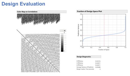
Target Customers & Partners
    Integrated Device Manufacturers                               Foundry

                                                                  Fabless

                                      Tool Suppliers (Partners)

                                           Atomera Incorporated             7
Customer Engagement & Revenue Model

    v                                               Customer Wafer Manufacturing

                                Atomera MST® Deposition                               Customer MST® Deposition

          1. Planning    2. Setup              3. Integration              4. Installation   5. Qualification   6. Production
  Phase

                        Engineering Service         •   MST deposition on customer wafers
                               Fees                 •   Integration consulting

                                                                       •    Integration licenses
                                              License Fees             •    Manufacturing licenses
                                                                       •    Distribution licenses

                                                  Joint Development Agreements                                   Royalties

                                               Atomera Incorporated                                                      8
Customer Pipeline

                              Number of Customer Engagements
        27
        24
        21
        18
        15
        12
         9
         6
         3
         0
             IPO 3Q 4Q 1Q 2Q 3Q 4Q 1Q 2Q 3Q 4Q 1Q 2Q 3Q 4Q 1Q 2Q 3Q 4Q 1Q
                 16 16 17 17 17 17 18 18 18 18 19 19 19 19 20 20 20 20 21^
                               Phase 1    Phase 2         Phase 3     Phase 4
•   19 customers, 25 engagements
                                                                                • At least 10 of the top 20 (IC Insights, McClean Report 2021)
•   Working with 50% of the world’s top semiconductor makers*                   ^ Updated March 2, 2021

                                               Atomera Incorporated                                                           9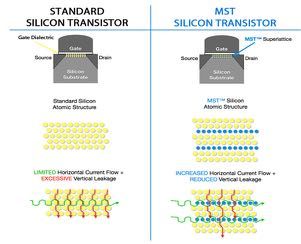
Royalty Opportunity
  ►   ~370 wafer fabs operating worldwide

  ►   Adoption of MST in one fab can make Atomera profitable from royalties alone
        § 2021 non-GAAP OPEX guidance is $14.00-14.5M

        Example 1 | Worldwide Average Fab                                 Example 2 | Leading Foundry, 28nm Fab
  Monthly Fab Capacity1                                             Monthly Fab Capacity
                                              49,000                                                        80,000
  (wafers/month)                                                    (wafers/month)

  Industry average wafer ASP - 2018           $1,136                Industry average 28nm wafer ASP         $3,000

  Annual Revenue Potential2                   $13M                  Annual Revenue Potential2               $58M

  Annual Revenue at 50% of ramp2              $6.7M                 Annual Revenue at 50% of ramp2          $29M

                          1. Represents wafers starts per month (200mm equiv) – 217.3M starts in 370 fabs
                          2. Assumes 2% royalty rate
                          Source: IC Insights Global Wafer Capacity 2019-2023 report, McClean Report 2019

                                                         Atomera Incorporated                                        10
MST Customer Business Opportunity
► Standard industry fab wafer pricing, GM, and cost
GM$ MST
Price GM% Increase Royalty Cost
28nm HP wafer $ 3,000 45% $ - $ - $ 1,650
28nm HP+ wafer $ 3,150 $150 price increase for +15% performance
► Fab gets a 30% performance improvement or 25% shrink via MST
MST processing cost $ 20 Incremental cost of depositing MST
28nm HP wafer with MST $ 3,300 47.4% $ 214 $ 66 $ 1,736 $300 price increase for +30% performance
28nm HP wafer with MST $ 3,375 48.5% $ 288 $ 68 $ 1,738 12.5% price increase for 25% size reduction
► Fabless customer benefit in die shrink case
Chip sales/ GM$ Product
wafer* GM% Increase ASP Die/wafer
2
28nm HP wafer $ 8,400 50.0% $ - $ 4.42 2,235 Baseline business for 30mm chip
28nm HP wafer with MST $ 11,279 62.8% $ 2,879 $ 4.42 3,001 Improved financials with 25% size reduction
► Everyone in the value chain benefits from MST technology
* Yielded
Atomera Incorporated 11Cash Efficient Growth
27
19
24
21 17
Customer Engagements
TTM Cash Burn ($M)
18 15
15 13
12
11
9
9
6
3 7
0 5
IPO 3Q 4Q 1Q 2Q 3Q 4Q 1Q 2Q 3Q 4Q 1Q 2Q 3Q 4Q 1Q 2Q 3Q 4Q
16 16 17 17 17 17 18 18 18 18 19 19 19 19 20 20 20 20
Phase 1 Phase 2 Phase 3 Annual cash burn
Atomera Incorporated 12Financial Review
FY 2019 Q1 '20 Q2 '20 Q3 '20 Q4 '20 FY 2020 Balance Sheet 12/31/20
GAAP Results Cash $37.9M
Revenue $0.53M $0.06M $ - $ - $ - $0.06M Debt -
Gross Profit $0.28M $0.05M $ - $ - $ - $0.05M Shares Outstanding 22.4M
Operating Expense
R&D $7.7 $2.1M $2.1M $2.0M $2.2M $8.4M
G&A $5.2 $1.4M $1.5M $1.3M $1.4M $5.6M
S&M $1.0 $0.2M $0.2M $0.2M $0.3M $0.9M
Total Operating Expense $13.9M $3.7M $3.8M $3.6M $3.9M $15.0M
Net Loss ($13.3M) ($3.6M) ($3.8M) ($3.6M) ($3.9M) ($14.9M)
Loss Per Share ($0.84) ($0.22) ($0.21) ($0.19) ($0.19) ($0.79)
Reconciliation between GAAP & Non-GAAP
Net Loss (GAAP) ($13.3M) ($3.6M) ($3.8M) ($3.6M) ($3.9M) ($14.9M)
Stock-Based Compensation $2.9M $0.6M $0.8M $0.8M $0.8M $3.0M
Warrant Modification - $0.1M - - - $0.1M
Other income (expense) ($0.3M) - - - - $0.1M
Adjusted EBITDA (Non-GAAP)* ($10.7M) ($2.9M) ($3.0M) ($2.7M) ($3.0M) ($11.7M)
* Adjusted EBITDA is a non-GAAP financial measure. A full reconciliation of GAAP and non-GAAP results is contained in our press release. Some totals reflect rounding
Atomera Incorporated 13Summary
► High margin, recurring revenue financial model
► Strong technology, patent position, and balance sheet
► Traction with many top industry players and growing licensee base
► Ramping commercial license revenues
Atomera Incorporated 14Thank You Atomera Incorporated 15
Backup Slides

    Atomera Incorporated   16
Joint Development Agreements
► Advantages of joint development
§ Atomera and customer engineers aligned on common goal
§ Customer “resident expert” team develops expertise on Atomera technology
§ Resident experts become natural advocates
► First JDA signed with market leading semiconductor company
§ Includes a manufacturing license, putting them in Phase 4
§ Upon completion, MST can more easily be adopted by business units
§ Each business unit is an incremental licensing opportunity
Atomera Incorporated 17Atomera MSTcad™
► Leading
semiconductor companies use
TCAD to model manufacturing processes
► MSTcad is an add-on for MST
► MSTcadcan optimize complex statistical
experiments to assess impact of multiple
manufacturing options
► Lowers cost of MST evaluation
► Accelerates time to successful results by
customers
Atomera Confidential 18MST: Mears Silicon Technology
Quantum Engineered Silicon
Partial Monolayers of MST Enhanced
Oxygen in Silicon Transistors
Supported by
Major Semiconductor
Tool Suppliers
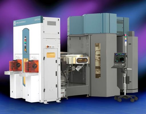
Atomera Incorporated 19300mm Epi Tool
Source: The McClean Report - 2019
300mm Epi Deposition Tool
Atomera Incorporated 20Atomera MSTcad™ Progress
► Leading semiconductor companies
use TCAD
► MST is modelled with a TCAD add-on
called MSTcad
► These plots show silicon verification of
MSTcad simulations
► Enables good electrical match-up for
5V NMOS and MST SP
► Should speed time to successful
results with customers
Atomera Incorporated 21Atomera Licensees
Large fabless
RF semiconductor
company
Atomera Incorporated 22MST1 vs MST2
► MST1
§ Blanket technology
§ Easy to integrate
§ Deposited at beginning of mfg process
§ Degraded by high heat in STI/Well module
§ Faster time to market for low heat processes
§ Used for FinFET, RFSOI, newer process nodes
► MST2
§ Selective technology
• Integrated after STI/Well so avoids highest heat
§ More flexible to apply to selected areas only
§ Used for 5V, Analog, older process nodes
Atomera Incorporated 235V Analog Breakthrough
► 3. Breakthrough performance achieved on 5V analog products
► Large segment of the overall analog market
► Atomera has targeted ~20% improvement on 5V devices
► In April Atomera demonstrated a 50%+ improvement
§ Using MST-SP technology
§ Relatively fast and easy to implement
► Expected to give many business advantages
§ Time to license, accelerated time to royalty, negotiating leverage
§ Applicable to even more markets
► Market size: ~$33B, or $660M in royalties
Atomera Incorporated 24MST-SP Progress
MST SP Progress
3.0
2.5
2.0
RSP 1.5
2
(mΩ-mm )
1.0
0.5
0.0
Feb-19 May-19 Aug-19 Dec-19 Mar-20 Jun-20 Sep-20
Control MST SP Industry Top Runner
Atomera Incorporated 25MST Matching Performance
35
► Transistor mismatch is an industry problem Si control
30
► Certaincircuit designs benefit from mismatch MST process
25
reduction
Better Matching
§ A-D convertors 20
σΔVth [mV]
§ SRAM
15
§ Flash
10
§ DRAM sense amplifiers
► MST can reduce mismatch by more than 50% 5
1.8V NMOS data
► Details available at Atomera’s website 0
0 1 2 3 4
§ blog.atomera.com 1/(WL)^0.5 [1/μm]
Smaller Devices
Atomera Incorporated 26You can also read