Kinetics of the thermal reduction process in graphene oxide thin films from in-situ transport measurements
←
→
Page content transcription
If your browser does not render page correctly, please read the page content below
Materials Research Express

PAPER • OPEN ACCESS

Kinetics of the thermal reduction process in graphene oxide thin films
from in-situ transport measurements
To cite this article: M winiarski et al 2021 Mater. Res. Express 8 015601

View the article online for updates and enhancements.

                              This content was downloaded from IP address 194.29.175.187 on 16/02/2021 at 08:18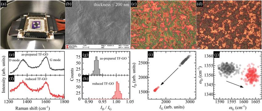
Mater. Res. Express 8 (2021) 015601 https://doi.org/10.1088/2053-1591/abdc50
PAPER
Kinetics of the thermal reduction process in graphene oxide thin
films from in-situ transport measurements
OPEN ACCESS
RECEIVED
30 October 2020
M Świniarski∗ , A Wróblewska , A Dużyńska , M Zdrojek and J Judek∗
REVISED
7 January 2021
Faculty of Physics, Warsaw University of Technology, Koszykowa 75, 00-662 Warszawa, Poland
∗
Authors to whom any correspondence should be addressed.
ACCEPTED FOR PUBLICATION
15 January 2021 E-mail: michal.swiniarski@pw.edu.pl and jaroslaw.judek@pw.edu.pl
PUBLISHED
Keywords: graphene oxide, reduction process, in-situ characterization
27 January 2021
Supplementary material for this article is available online
Original content from this
work may be used under
the terms of the Creative
Commons Attribution 4.0 Abstract
licence. We investigate the influence of the thermal annealing process on the transport properties of thin films made
Any further distribution of
this work must maintain
of graphene oxide. Specially developed methodology allows us to demonstrate that the thermal annealing
attribution to the process of graphene oxide thin films can be described as a kinetic process with one activation energy, which
author(s) and the title of
the work, journal citation equals 0.94 eV±0.12 eV. Moreover, we show that the electrical transport mechanism evolves with the
and DOI.
annealing temperature (reduction level) of GO thin films. We have noticed that the Variable Range Hopping
transport model change from 3D, 2D to Efros-Shklvoskii with a reduction level. Our findings contribute to
further understanding of the role of kinetics in thermal reduction processes of thin films made of graphene
oxide and could be useful in applications in which electrical parameters need to be tuned.
1. Introduction
Graphene oxide (GO) is a highly defected (oxidized) and nonconductive version of graphene [1, 2]. It possesses a
few interesting features such as: (a) well-established production method taking abundantly occurring graphite
crystal as a substrate [3–5]; (b) presence of hydroxyl and carboxyl groups [6–10], which could act as reactive
centers for a variety of surface-modification reactions enabling, e.g., polymer composite formation [11, 12];
(c) excellent water solubility [13–15] and high adhesion between flakes allowing for efficient thin-film production
[16]; (d) tunable photoluminescence [17], carrier recombination time ranging from approximately 1 ps to above
300 ps [18], and saturable absorption [19] , which make GO an interesting material for ultrafast photonic
applications. Moreover, through the chemical [20, 21] or thermal [22–24] treatment as well as through the
irradiation by the electron beam [25, 26] or by the UV light [27], graphene oxide can be easily transformed into
another important version of graphene—reduced graphene oxide (rGO) [28]. Such an indirect route of graphene
fabrication through the intermediate GO phase is considered very attractive because it combines advantages of GO
related to facile production and processing, and unique properties of graphene received in the end material after
reduction. Formally, the reduction process consists of removal of some amount of functional groups containing
oxygen (e. g., hydroxyl, carboxyl, epoxy) from the honeycomb carbon lattice. The reduction process leads to partial
restoration of the pristine graphene properties [29], like conductivity and hydrophobicity, despite still large
amount of structural defects.
This directly paves way to these graphene-based applications in which outstanding electrical parameters are
not crucial [30], like transparent electrodes [23, 24] or print [31, 32].
First works on transport properties of graphene oxide during thermal annealing were published by Jung et al
[22, 33, 34], who examined individual single-layer and multi-layer GO platelets obtained through the wet exfoliation
method. The analysis of the electrical resistivity versus time in temperatures led to the conclusion that below 180 °C
the thermal reduction process can be described as a kinetic process with the activation energy of 1.6 eV mol−1.
Moreover, the analysis of results from temperature programmed desorption experiment provided information
that decomposition of graphene oxide begins at temperature equaling approximately 70 °C. Among desorbing
gases, apart from expected O2 and H2O, there are also CO2 and CO, presence of which unfortunately means that
© 2021 The Author(s). Published by IOP Publishing Ltd
Mater. Res. Express 8 (2021) 015601 M Świniarski et al
undesirable carbon loss occurs during annealing. What is important, most of these results have been further
confirmed by other groups using, e.g., differential scanning calorimeter technique [35, 36].
In this study, we focus on further deepening of our understanding of the reduction mechanisms of thin films
made of graphene oxide induced by elevated temperatures, and on their link to changes in transport properties
during thermal annealing. We note that in contrary to previously published reports [22, 33, 34], here we examine
thin film made of graphene oxide, thus we are not studying properties of individual platelets, but homogenous films
with lateral dimensions of few mm and thickness of 200 nm. Such films are much more complicated physical
systems than individual single- or multi-layered flakes. The macroscopic conductivity consists of conduction of
individual flakes part and conduction between adjacent flakes, which is ruled by their arrangement.
Therefore, the possibility of formation of percolation paths, the conduction through the interfaces, and
changes in both during annealing should be embraced. Moreover, gas desorption occurring at elevated
temperatures might lead to changes in film morphology, having a great impact on the distribution of the
conduction paths and properties of the interfaces, which directly result from the morphology. For example, part
of the desorbed gases could form a ‘bubble’ within the thin film that will locally loosen the thigh arrangement of
the flakes leading directly to a further decrease in electrical conduction.
Changes in transport properties of thin films made of GO during annealing have been barely studied, existing
literature is limited to remarks about sudden decrease in the resistivity value and its further stabilization in time
[37–39]. Here, on the contrary, we pay special attention to the first moments of the thermal annealing process. We
demonstrate that analysis of temporal changes in resistivity while a set of thin films made of GO is exposed to
different elevated temperatures allows us to conclude that, surprisingly, the thermal reduction can be described as the
kinetic process with one activation energy, that equals 0.94 eV±0.12 eV. We note that we adopted a more strict
methodology than in the works of Jung et al [22, 33, 34], that the unit of our result is eV not eV per mole or molecule,
and that the value of the energy activation is in agreement with theoretical calculations on the GO reduction process
[40–42]. We show that Variable Range Hopping (VRH) transport models are the predominant transport models in
our thin films [43–49]. Moreover, we have noticed that the electrical transport model evolves with the reduction level
of our GO thin films. Samples reduced in lower temperatures (450 K–475 K) shows 3D and 2D-VRH model, while
samples with higher reduction level (490 K–500 K) are well described by the Efros-Shklovskii model (ES-VRH).
2. Experimental
Graphene oxide thin films were fabricated by the vacuum filtration method [50] from commercially available
GO solution in water (concentration of 4 mg/ml, Graphenea Inc.). The lateral dimensions of all GO thin films
are about 5 mm×5 mm, whereas their thicknesses are about 200 nm. Because all films are completely
mechanically unstable, we deposited them on popular 10 mm×10 mm low resistivity silicon substrates with
thermally grown silicon dioxide (SiO2) . To make good/stable electrical contacts we evaporated 100 nm-thick
palladium electrodes at the four edges of the GO films. Palladium film was deposited using a thermal
evaporation system (Kurt J Lesker Nano 36) and mechanical mask. The mechanical mask approach has been
chosen to ensure that we have got as clean samples as possible. The lithographic process for producing metal
contacts requires using polymers, which should be annealed, and the additional chemical treatment in the
developing process. Samples prepared this way were attached and bonded to an electrical adapter and placed
inside Oxford MicrostatHe2 cryostat. One of the samples just before the measurements is shown in figure 1(a).
Before and after the thermal reduction process we made some structural investigations. SEM image shown
in figure 1(b) illustrates a smooth and continuous GO surface. The optical images of the GO samples before and
after the thermal reduction process are shown in figures 1(c) and (d). In figures 1(e) and (f) we present typical
Raman spectra of our samples, which prove that we investigate a highly disordered form of carbon [51]. We can
observe the D (defect-induced) and G (signature of the sp2 carbon) modes, and no 2D (related to the quality of
the sp2 carbon lattice) mode. Statistical distributions of the ratio of the intensity of the D mode ID to the intensity
of the G mode IG before and after the thermal reduction process are shown in figures 1(g) and (h). A significant
increase in the ID/IG ratio that is seen, could be related to further damage of the hexagonal carbon lattice upon
thermal treatment [50]. Figure 1(i) shows the intensity of the D mode ID versus the intensity of the G mode IG
before and after the thermal reduction process. What can be concluded is the linear dependence between ID and
IG and much lower Raman signal intensity after the thermal reduction process. The latter information means
that carbon loss in the examined thin film is highly probable. Figure 1(j) shows a correlation analysis between the
position of the D mode ωD and G mode ωG. Assuming that position of the D mode is approximately 2 times
smaller than 2D mode [52], we can use the vector decomposition method [53] to conclude that thermal
annealing results in an increase in doping whereas not affecting the strain.
Electrical measurements of the sheet resistance RS value were performed in the van der Pauw configuration
[54] with Keithley SMU 2450, National Instruments PCI-6281 acquisition card, and Keithley 7001 switch
2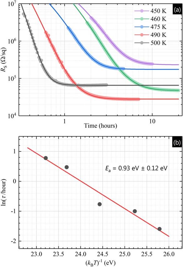
Mater. Res. Express 8 (2021) 015601                                                                                      M Świniarski et al

   Figure 1. (a) Picture of the experimental setup—sample bounded to electrical adapter in Oxford MicrostatHe2 cryostat. (b) SEM
   image of as-prepared GO sample. (c) and (d) Typical optical microscope pictures of GO before and after thermal reduction process.
   The white bar length is 10 μm. (e) and (f) Typical Raman spectra collected from as-prepared and thermally reduced GO samples.
   (g) and (h) Distributions of the intensity of the D mode to intensity of the G mode ratios from as-prepared and thermally reduced GO
   samples. (i) Correlation between intensity of the D mode versus intensity of the G mode from as-prepared and thermally reduced GO
   samples; significant decrease in the intensity is clearly observed. (j) Correlation between position of the D and G mode from as-
   prepared and thermally reduced GO samples indicating change in sample doping after thermal reduction process.

equipped with Keithley 7065 hall card. We carefully verified that our transport measurements do not lead to
structural changes in an object under investigations, like, e.g., in the case of Raman spectroscopy [55]. The
temperature of the samples was controlled through the Oxford Instruments Mercury iTC controller. Using the
Pt1000 sensor we carefully verified that the temperature set on the controller is equal to the temperature of the
silicon substrate surface in the whole 300 K–500 K temperature range.

3. Results and discussion

The main results of this paper are shown in figure 2(a), which illustrates the time evolution of the sheet resistance
RS of five thin films made of GO exposed to five elevated temperatures (450 K, 460 K, 475 K, 490 K, and 500 K) at
ambient atmosphere. Before we provide physical interpretation, we want to clarify a few unobvious issues. First,
we note that for each of the prepared samples we applied only one selected temperature that was constant during
the whole experiment (instead of stepwise temperature change like in works of Jung [22, 33, 34]). The main
advantage of such an approach is the same (or very similar) ‘starting point’ for the reduction process in all cases
because all the samples were fabricated from the same ‘batch’. The main drawback is the requirement of having a
set of very similar samples (the number of samples should be equal to the number of selected temperatures) and
a longer duration of the whole experiment. Secondly, for all samples value of the sheet resistance decreases in
time up to some level, afterwards it is approximately constant. Initial changes in RS depend on the temperature
of the annealing (the lower temperature the slower changes meaning slower reduction process), which is an
expected effect. The final value of sheet resistance does not follow the temperature trend, where we observed that
samples reduced in 460 K and 490 K do not fit into the pattern. This effect could be described as a difference in
the morphologies of the samples, which proves that it is a highly disordered material, especially when it is
reduced. We would like to remind that all samples are from the same filtration process, which should ensure that
morphologies are as similar as possible. Despite that, the conductivity distribution is no longer similar after the
reduction process.
     Third comment is related to the time scale which is limited and different for each of the temperatures. In the
performed experiment the acquisition of voltage and current values were continuous from the very beginning
up to the time the resistivity value has stabilized but no longer than 10 h. However, it can be seen that for each
trace there is no experimental data even at the beginning of the measurements. It is because all samples were
insulating after the fabrication process (a measurement of their resistance was beyond the technical possibility of
used instruments). During the reduction process, the current value systematically increased and in consequence,
at some point, the measured resistance value started to reflect the true sheet resistance of the sample. This effect
is nicely rendered as the shift of the first plotted experimental point versus the temperature of the annealing.
Selection of the moments from which we consider data reliable was made arbitrary. We also remark that in all
cases the elevated temperature was applied at the ‘zero’ time.

                                                        3
Mater. Res. Express 8 (2021) 015601 M Świniarski et al
Figure 2. (a) Samples’ sheet resistance during the first annealing at 450 K, 460 K, 475 K, 490 K, and 500 K. At the beginning the values
of sheet resistance of all samples were beyond the range of our measurement setup. When the samples became measurable, we started
recording obtained results. The color circles represent experimental data whereas the solid lines represent theoretical model.
(b) Extracted time constant values and fitted straight line, which slopes gives ‘averaged’ activation energy value.
Analysis of the reduction process reflected in changes in resistance requires some justified assumptions:
(1) we fabricated a set of very similar samples having very similar ‘starting point’; (2) energy of desorption of all
functional groups can be expressed as one averaged energy—we call it Ea; (3) Boltzmann statistic describes the
energy distribution among functional groups, which implies that probability of desorption of one ‘averaged’
functional group equals p1=exp(−Ea/kBT), where kB is Boltzmann constant and T means temperature; this
probability p1 is related to the time constant τ at which we observe the decrease in resistivity ρ; (4) number of
functional groups dN that is desorbing in unit time t is proportional to the current number of functional groups
N(t), i.e., dN=−N(t)·exp (−Ea/kBT); (5) resistivity of the GO flake ρ(t) is related to number of functional
groups N(t), i.e., N(t)–Nf∼lnρ(t)-lnρf, where Nf and ρf are residual values of the number of functional groups
and resistivity, after reduction [34, 56, 57]. Finally, we obtained the R(t) formula given by:
R (t ) = R 0 + Rf exp [b exp ( - t / t )] (1)
where R0 means the residual sheet resistance resulting for example from wires and contacts, β is the constant
value of proportionality factors and final concentration, Rf is the final value of resistance, τ is the time constant of
the thermal reduction process. Solid lines in figure 2(a) represent the theoretical dependence of the time function
of resistivity fitted to experimental data for five annealing temperatures. Excellent correspondence between
experiment and theory proves that the thermal reduction process of the thin film made of graphene oxide can be
described as a kinetic process with one activation energy. Moreover, this conclusion consists with theoretical
predictions, which underline the role of kinetics [41]. To calculate the value of the ‘averaged’ activation energy
we plotted in figure 2(b) logarithm of the time constant τ (obtained from fitting procedure to data from
figure 2(a)) versus (kBT)−1. The slope of the fitted straight line equals the ‘averaged’ activation energy
0.93 eV±0.12 eV, which results directly from the third assumption. This value is comparable with the value
reported by other authors. For example, Larciprete et al [40], who ‘identifies a dual path mechanism in the
thermal reduction of graphene oxide driven by the oxygen coverage’ report activation energies of 1.13 eV (DFT)
4Mater. Res. Express 8 (2021) 015601 M Świniarski et al
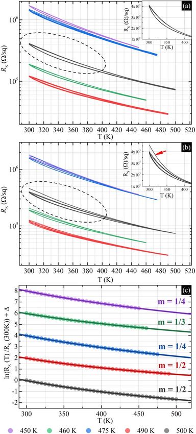
Figure 3. (a) Sheet resistance values during first (after annealing) temperature sweep. Traces are repeatable despite small hysteresis.
(b) Sheet resistance values during second (after wetting) temperature sweep. Traces are not repeatable. (c) Averaged, logarithmized,
normalized, and shifted traces from figure (a) with fitted curve representing fit for chosen power of VRH models.
and 1. 21 eV (TPD) at low oxygen concentration, and 1.10 eV (DFT) and 1.20 eV (TPD) at high oxygen
concentration.
The last question we analyze in this work is the conduction mechanism of thermally reduced thin films made of
GO. For this purpose we make measurements as a function of temperature, i.e., we measured RS for temperature
ranging from room temperature (RT) up to the temperature the sample was annealing at (AT). Such temperature
sweep was performed six times one after the other (AT→RT→AT→RT→AT→RT) just after annealing,
which is illustrated in figure 3(a), and once again the whole sequence a few hours later, which is illustrated in
figure 3(b). As can be seen, for all samples traces acquired just after annealing are repeatable despite small hysteresis
(the difference between results obtained when heating and when cooling). This means that samples are stable at
5Mater. Res. Express 8 (2021) 015601 M Świniarski et al
temperatures up to the temperature of the annealing; however, the temperature changes were too fast. On the other
hand, traces acquired a few hours after annealing are almost reversible. The most visible discrepancy occurs for the
first temperature sweep, but a smaller shift can be observed even for further sweeps. It is difficult to establish the
origin of this effect; however, we suspect that it could be the effect of water absorption. We note that water is often
observed compound during thermal desorption from graphene oxide.
For the analysis of the conduction mechanism we used averaged data from the first tarce (figure 3(a)) and fit
the variable range hopping model (figure 3(c)) expressed as:
R S (T ) = R S,0 + R S,1 exp [(T0 / T )m] , (2)
where RS means sheet resistance, RS,0 means the residual sheet resistance resulting from example from wires and
contacts, T0 is the Mott temperature, and m=1/(d+1), where d is the dimensionality of the conduction. The
electronic transport determination has been done by two methods described in the supplementary information.
We found out that the conduction transport model in our GO thin films evolves with reduction temperature,
which is related to the reduction level of our materials. The general trend could be described as a reduction of
dimensionality d with an increase of the annealing temperature. The samples reduced in temperatures 450 K,
460 K, and 475 K are well described by the 3D (m=1/4) and 2D-VRH (m=1/3). We note that the sample reduced
475 K were characterized by higher fluctuations, figure S1 (available online at stacks.iop.org/MRX/8/015601/
mmedia), which could be the reason of the m=1/4. Next, the samples reduced in higher temperatures are greatly
described by the Efros-Shklovskii VRH model (m=1/2). The lower fraction of the sp2/sp3 in GO thin-film
network causes the electrical charges to hop between localized states in 3 dimensions as expected for low reduced
GO films [46]. When sp2/sp3 fraction is increasing, the transport is mostly realized within the rGO flakes area,
changing the transport model from 3D to 2D. Further reduction leads to Efros-Shklovskii VRH model which take
into account the Coulomb interactions between charges hopping between localized states [43, 44].
4. Conclusions
We demonstrated that methodology proposed by us, i.e., transport measurements on a set of very similar
samples during annealing at different but constant temperatures, may justify that thermal annealing process of
thin films made of graphene oxide can be described as a kinetic process with one activation energy 0.93 eV±
0.12 eV. Moreover, we have noticed that the electrical transport model evolves with the annealing temperature
(reduction level) of GO thin films. The samples reduced in temperatures 450 K, 460 K ,and 475 K are described
by the 3D- and 2D-VRH models, while the reduction in higher temperatures (490 K and 500 K) resulted in the
Efros-Shklovskii VRH model. Our results are consisted with results obtained by other authors from other
experimental techniques or calculations, and further complements on the physics of graphene oxide compound
and thin films made of 2D materials.
Acknowledgments
This work was funded by the National Center for Research and Development, Poland, within Project No. Lider/
180/L-6/14/NCBR/2015 and TechMatStrateg1/347012/3/NCBR/2017.
Data availability statement
The data that support the findings of this study are available upon reasonable request from the authors.
ORCID iDs
M Świniarski https://orcid.org/0000-0003-3786-3785
A Wróblewska https://orcid.org/0000-0003-3728-1216
A Dużyńska https://orcid.org/0000-0001-8006-3914
M Zdrojek https://orcid.org/0000-0002-8897-6205
J Judek https://orcid.org/0000-0002-4326-7392
References
[1] Dreyer D R, Park S, Bielawski C W and Ruoff R S 2010 The chemistry of graphene oxide Chem. Soc. Rev. 39 228–40
[2] Compton O C and Nguyen S T 2010 Graphene oxide, highly reduced graphene oxide, and graphene: versatile building blocks for
carbon-based materials Small 6 711–23
6Mater. Res. Express 8 (2021) 015601 M Świniarski et al
[3] Brodie B.C. 1859 XIII. On the atomic weight of graphite Philos. Trans. R. Soc. London 149 249–59
[4] Staudenmaier L 1898 Verfahren zur Darstellung der Graphitsäure Berichte der Dtsch. Chem. Gesellschaft 31 1481–7
[5] Hummers W S and Offeman R E 1958 Preparation of graphitic oxide J. Am. Chem. Soc. 80 1339–1339
[6] Hontoria-Lucas C, López-Peinado A J, de D López-González J, Rojas-Cervantes M L and Martín-Aranda R M 1995 Study of oxygen-
containing groups in a series of graphite oxides: physical and chemical characterization Carbon NY 33 1585–92
[7] He H, Riedl T, Lerf A and Klinowski J 1996 Solid-state NMR studies of the structure of graphite oxide J. Phys. Chem. 100 19954–8
[8] Lerf A, He H, Riedl T, Forster M and Klinowski J 1997 13C and 1H MAS NMR studies of graphite oxide and its chemically modified
derivatives Solid State Ionics 101–103 857–62
[9] He H, Klinowski J, Forster M and Lerf A 1998 A new structural model for graphite oxide Chem. Phys. Lett. 287 53–6
[10] Lerf A, He H, Forster M and Klinowski J 1998 Structure of graphite oxide revisited J. Phys. Chem. B 102 4477–82
[11] Stankovich S, Piner R D, Nguyen S B T and Ruoff R S 2006 Synthesis and exfoliation of isocyanate-treated graphene oxide nanoplatelets
Carbon NY 44 3342–7
[12] Stankovich S et al 2006 Graphene-based composite materials Nature 442 282–6
[13] Hirata M, Gotou T, Horiuchi S, Fujiwara M and Ohba M 2004 Thin-film particles of graphite oxide: I. High-yield synthesis and
flexibility of the particles Carbon N. Y. 42 2929–37
[14] Titelman G I, Gelman V, Bron S, Khalfin R L, Cohen Y and Bianco-Peled H 2005 Characteristics and microstructure of aqueous
colloidal dispersions of graphite oxide Carbon NY 43 641–9
[15] Konios D, Stylianakis M M, Stratakis E and Kymakis E 2014 Dispersion behaviour of graphene oxide and reduced graphene oxide
J. Colloid Interface Sci. 430 108–12
[16] Dikin D A et al 2007 Preparation and characterization of graphene oxide paper Nature 448 457–60
[17] Xin G et al 2012 Tunable photoluminescence of graphene oxide from near-ultraviolet to blue Mater. Lett. 74 71–3
[18] Kaniyankandy S, Achary S N, Rawalekar S and Ghosh H N 2011 Ultrafast relaxation dynamics in graphene oxide: evidence of electron
trapping J. Phys. Chem. C 115 19110–6
[19] Zhao X et al 2011 Ultrafast carrier dynamics and saturable absorption of solution-processable few-layered graphene oxide Appl. Phys.
Lett. 98 121905
[20] Gilje S, Han S, Wang M, Wang K L and Kaner R B 2007 A chemical route to graphene for device applications Nano Lett. 7 3394–8
[21] Gómez-Navarro C et al 2007 Electronic transport properties of individual chemically reduced graphene oxide sheets Nano Lett. 7
3499–503
[22] Jung I, Dikin D A, Piner R D and Ruoff R S 2008 Tunable electrical conductivity of individual graphene oxide sheets reduced at ‘Low’
temperatures Nano Lett. 8 4283–7
[23] Wang X, Zhi L and Müllen K 2008 Transparent, conductive graphene electrodes for dye-sensitized solar cells Nano Lett. 8 323–7
[24] Becerril H A, Mao J, Liu Z, Stoltenberg R M, Bao Z and Chen Y 2008 Evaluation of solution-processed reduced graphene oxide films as
transparent conductors ACS Nano 2 463–70
[25] Kim S et al 2015 Localized conductive patterning via focused electron beam reduction of graphene oxide Appl. Phys. Lett. 106 133109
[26] Wu K H et al 2015 Electron-beam writing of deoxygenated micro-patterns on graphene oxide film Carbon NY 95 738–45
[27] Ding Y H, Zhang P, Zhuo Q, Ren H M, Yang Z M and Jiang Y 2011 A green approach to the synthesis of reduced graphene oxide
nanosheets under UV irradiation Nanotechnology 22 21560
[28] Gómez-Navarro C et al 2010 Atomic structure of reduced graphene oxide Nano Lett. 10 1144–8
[29] Bourlinos A B, Gournis D, Petridis D, Szabó T, Szeri A and Dékány I 2003 Graphite oxide: chemical reduction to graphite and surface
modification with primary aliphatic amines and amino acids Langmuir 19 6050–5
[30] Tung V C, Allen M J, Yang Y and Kaner R B 2009 High-throughput solution processing of large-scale graphene Nat. Nanotechnol. 4
25–9
[31] Rogala M et al 2015 The role of water in resistive switching in graphene oxide Appl. Phys. Lett. 106 263104
[32] McManus D et al 2017 Water-based and biocompatible 2D crystal inks for all-inkjet-printed heterostructures Nat. Nanotechnol. 12
343–50
[33] Jung I, Dikin D, Park S, Cai W, Mielke S L and Ruoff R S 2008 Effect of water vapor on electrical properties of individual reduced
graphene oxide sheets J. Phys. Chem. C 112 20264–8
[34] Jung I et al 2009 Reduction kinetics of graphene oxide determined by electrical transport measurements and temperature programmed
desorption J. Phys. Chem. C 113 18480–6
[35] Yin K et al 2011 Thermodynamic and kinetic analysis of low- temperature thermal reduction of graphene oxide citation Nano-Micro
Lett 3 51–5
[36] Qiu Y, Collin F, Hurt R H and Külaots I 2016 Thermochemistry and kinetics of graphite oxide exothermic decomposition for safety in
large-scale storage and processing Carbon NY 96 20–8
[37] Zangmeister C D 2010 Preparation and evaluation of graphite oxide reduced at 220 °C Chem. Mater. 22 5625–9
[38] Mattevi C et al 2009 Evolution of electrical, chemical, and structural properties of transparent and conducting chemically derived
graphene thin films Adv. Funct. Mater. 19 2577–83
[39] Chen X et al 2016 Rapid thermal decomposition of confined graphene oxide films in air Carbon N. Y. 101 71–6
[40] Larciprete R, Fabris S, Sun T, Lacovig P, Baraldi A and Lizzit S 2011 Dual path mechanism in the thermal reduction of graphene oxide
J. Am. Chem. Soc. 133 17315–21
[41] Lu N, Yin D, Li Z and Yang J 2011 Structure of graphene oxide: thermodynamics versus kinetics J. Phys. Chem. C 115 11991–5
[42] Zhou S and Bongiorno A 2013 Origin of the chemical and kinetic stability of graphene oxide Sci. Rep. 3 2484
[43] Chuang C et al 2012 Experimental evidence for Efros–Shklovskii variable range hopping in hydrogenated graphene Solid State
Commun. 152 905–8
[44] Joung D and Khondaker S I 2012 Efros-Shklovskii variable-range hopping in reduced graphene oxide sheets of varying carbon sp2
fraction Physical Review B 86 235423
[45] McIntosh R, Mamo M A, Jamieson B, Roy S and Bhattacharyya S 2012 Improved electronic and magnetic properties of reduced
graphene oxide films EPL Europhysics Lett. 97 38001
[46] Venugopal G, Krishnamoorthy K, Mohan R and Kim S-J 2012 An investigation of the electrical transport properties of graphene-oxide
thin films Mater. Chem. Phys. 132 29–33
[47] Baek S J et al 2014 The effect of oxygen functional groups on the electrical transport behavior of a single piece multi-layered graphene
oxide Synth. Met. 191 1–5
[48] Muchharla B, Narayanan T N, Balakrishnan K, Ajayan P M and Talapatra S 2014 Temperature dependent electrical transport of
disordered reduced graphene oxide 2D Mater. 1 1–9
7Mater. Res. Express 8 (2021) 015601 M Świniarski et al
[49] Kim H-J et al 2015 Charge transport in thick reduced graphene oxide film J. Phys. Chem. C 119 28685–90
[50] Wróblewska A et al 2017 Statistical analysis of the reduction process of graphene oxide probed by Raman spectroscopy mapping J. Phys.
Condens. Matter 29 475201
[51] Ferrari A C and Robertson J 2000 Interpretation of Raman spectra of disordrred and amorphous carbon Phys. Rev. B 61 14 295
[52] Judek J, Pasternak I, Dabrowski P, Strupinski W and Zdrojek M 2019 Hydrogen intercalation of CVD graphene on germanium (001)—
strain and doping analysis using Raman spectroscopy Appl. Surf. Sci. 473 203–8
[53] Lee J E, Ahn G, Shim J, Lee Y S and Ryu S 2012 Optical separation of mechanical strain from charge doping in graphene Nat. Commun.
3 1024
[54] van der Pauw L J 1958 A method of measuring the resistivity and Hall coefficient on lamellae of arbitrary shape Philips Tech. Rev. 20
220–4
[55] Mehta J S, Faucett A C, Sharma A and Mativetsky J M 2017 How reliable are raman spectroscopy measurements of graphene oxide?
J. Phys. Chem. C 121 16584–91
[56] Boukhvalov D W and Katsnelson M I 2008 Modeling of graphite oxide J. Am. Chem. Soc. 130 10697–701
[57] Yan J-A, Xian L and Chou M Y 2009 Structural and electronic properties of oxidized graphene Phys. Rev. Lett. 103 086802
8You can also read