Drude Relaxation Rate in Grained Gold Nanoantennas
←
→
Page content transcription
If your browser does not render page correctly, please read the page content below
pubs.acs.org/NanoLett

Drude Relaxation Rate in Grained Gold
Nanoantennas
Kuo-Ping Chen, Vladimir P. Drachev,* Joshua D. Borneman, Alexander V. Kildishev, and
Vladimir M. Shalaev
Birck Nanotechnology Center and School of Electrical and Computer Engineering, Purdue University, 1205 West
State Street, West Lafayette, Indiana 47907

   ABSTRACT The effect of grain boundaries on the electron relaxation rate is significant even for large area noble metal films and
   more so for plasmonic nanostructures. Optical spectroscopy and X-ray diffraction show a substantial improvement in plasmon
   resonance quality for square-particle nanoantennas after annealing due to an enlarged grain size from 22 to 40 nm and improved
   grain boundaries described by the electron reflection coefficient. The electron relaxation rate due to the grains is shown to decrease
   by a factor of 3.2.

   KEYWORDS Plasmonics, nanoantennas, electron relaxation rate, grain structure, annealing

N         anoantennas formed by coupled noble metal par-                  We have determined both the Drude relaxation rate from
          ticles enable the plasmon resonance and strong                  optical transmission and reflection measurements and the
          enhancement of the local electromagnetic field in               grain properties from the X-ray diffraction (XRD) measure-
the gap which can be tuned to different frequencies.1 The                 ments. To analyze the results of our experiments, we use a
localized surface plasmon resonances and highly confined                  quantitative model based on the linearized Boltzmann equa-
electromagnetic fields produced by nanoantennas make
                                                                          tion.11
possible many applications including nanometer-scale pho-
tolithography,2 nonlinear optics,3 biosensors, optical trap-                  Many previous works have shown that annealing im-
ping, solar energy harvesting, fluorescence enhancement,4,5               proves the quality of large area metal films.6,7,12,13 However,
and improved near-field scanning optical microscopy. Gold                 we have found that this is not always true for metal nano-
and silver are appropriate plasmonic materials for the visible            structures. Specifically, annealing does not improve the
range due to their low electron relaxation rates, high plasma             quality of high aspect ratio nanostructures, such as nanos-
frequency, and high-frequency interband transitions.6,7 Al-               trips with a width less than 80 nm. Moreover, heating high
though silver has a lower electron relaxation rate than gold,             aspect ratio structures initiates structural Rayleigh instability,
gold is widely used, especially in biological applications or             resulting in segmentation into randomly sized pieces. In this
fluidic environment experiments due to biocompatibility                   paper we present nanostructures whose resonance proper-
and higher chemical stability.8
                                                                          ties can be substantially improved through annealing. The
    Overall, the parameter of greatest interest is the Drude
                                                                          plasmon resonance width is affected by the change in
relaxation rate Γ, which is inversely proportional to the
                                                                          electron relaxation rate. Another potential reason could be
intraband electron relaxation time τ at optical frequencies,
i.e., Γ ) hτ-1, where h is Planck’s constant, and which is the            inhomogeneous broadening due to the geometrical effect of
primary parameter quantifying the nanoantenna resonance                   roughness as we observed in our previous paper14 for paired
quality. Typically, decreased resonance quality due to grain              strips. This effect is less contributive due to better quality of
boundary effect is either commented on, but not addressed,                the square shape particles. It is shown that the decrease in
in the literature or is invoked qualitatively. For nanostruc-             the electron relaxation rate correlates with an increase in
tures, this effect is less studied but typically more important           the mean crystalline size, as measured by X-ray diffraction.
than for large area metal films, because of the more com-                 Additionally, our analysis based on a grain boundary scat-
plicated fabrication procedure.9 The effect of grains on the              tering model11 shows that the strength of the potential
surface-plasmon polariton propagation length was studied                  barriers at the grain boundaries, expressed in terms of
recently,10 but the grain size there was determined from                  electron reflection coefficient, is also reduced after annealing.
atomic force microscopy images, which usually give a rough
estimate since it does not probe an intrinsic grain structure.               During fabrication, many factors affect the resulting
                                                                          quality of the gold nanoantenna and therefore change the
                                                                          dielectric constant of gold. The resulting gold dielectric
* Corresponding author, vdrachev@purdue.edu.
Received for review: 11/6/2009
                                                                          constant may be calculated using the Drude-Lorentz model
Published on Web: 02/03/2010                                              in eq 1

      © 2010 American Chemical Society                              916                        DOI: 10.1021/nl9037246 | Nano Lett. 2010, 10, 916–922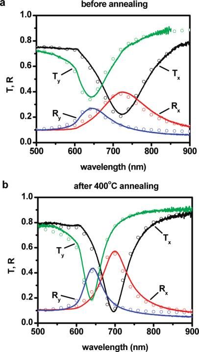
ωp2                        fmωm2                   annealing treatment. Additionally the reason for improve-
     ε)1-
                 ω + iαΓpω
                   2
                                  +     ∑ω   2
                                                 - ω - iΓmω
                                                    2                     ment of the plasmonic resonance will be discussed.
                                        m   m                                 Our gold nanoantenna structures are fabricated on a 15
                                                              (1)         nm indium-tin-oxide (ITO)-coated glass substrate. For
                                                                          E-beam lithography, PMMA A2 (MicroChem Corp.) photo-
    The Drude-Lorentz model has two terms: the Drude                      resist is spin-coated onto the ITO glass substrate at 3000 rpm
term for the free-electron resonance, and the sum of the                  for 60 s. Following a 1 h prebake of the photoresist at 160
Lorentz terms, representing interband transitions. Here ωp                °C, an E-beam direct writing system (Vistec) is used to define
is the plasmon frequency and Γp is the damping constant                   the pattern with 100 kV, 765 pA, and 800 uC/cm2. Methyl
for the Drude term. R is a loss factor used to quantify the               isobutyl ketone (MIBK)/isopropanol (IPA) (1:3) is used to
difference between the damping term in bulk from the                      develop the photoresist for 45 s and O2 plasma ashing
literature7 and our fabricated sample. Lattice defects and                (Branson) at 100 W for 5 s is used for the descum process
grain boundaries will increase the damping constant, be-                  to remove residual photoresist for improved lift-off. Then,
cause the total damping term (Γp) is the sum of the collision             electron beam evaporation is used to produce a 5 nm
rate from electrons-electrons, electrons-phonons, and                     adhesion layer of titanium and a 30 nm gold film with a 0.5
electron-grain boundaries. Therefore, film defects increase               Å/s deposition rate in a 7 × 10⁻⁷ Torr vacuum chamber
the gold damping constant, quantified as having a larger R.               (Airco). After film deposition, lift-off is performed by immer-
As this work will show, the internal damping may be reduced               sion in Remover PG (MicroChem Corp.) for 6 h.
by annealing the sample after fabrication in order to enlarge                 Following fabrication, annealing is done using both a hot
the grains and reduce the number of grain boundaries.                     plate and a rapid thermal processing system (RTP, Minipulse
Potentially, surface roughness may also increase the relax-               RTA), for 2 min, at 12 different temperatures from room
ation rate of electrons. However, three-dimensional simula-               temperature (20 °C) up to 400 °C. After annealing, the far-
tions of nanoantenna roughness, which will be discussed                   field transmission and reflection spectra are measured for
later, and previous simulations and experiments for two-                  both the primary (x), E-field perpendicular to the antenna
dimensional magnetic gratings with a root-mean-square                     gap, and for the secondary (y) polarization, E-field parallel
(rms) roughness of up to 6 nm,14 show little change in the                to the gap. FE-SEM (Hitachi S-4800) and AFM (Veeco Dimen-
relaxation rate as a function of roughness.                               sion) measurements are used in order to profile the surface
    Because gold square-particle nanoantennas have a strong               structure and roughness. XRD (PANalytical X’Pert) θ/2θ
coupled plasmonic resonance, spectra that can be well                     deflection measurement is used to obtain the average grain
matched using numerical simulations, and a low aspect                     size.
ratio, this work uses gold nanoantennas to examine the                        Figure 1a shows the nanoantenna design. The square
effect of different annealing temperatures. The annealing                 particle dimensions are 100 nm × 100 nm with a thickness
process has been widely used in the semiconductor industry                of 30 nm. The gap between the particles is 30 nm, and the
and for thin-film fabrication for decades. In thin-film fabrica-          period is 400 nm in both the x and y directions. The FE-SEM
tion, the main purpose of annealing is to decrease the                    image in Figure 1b shows not only the good lift-off condition
intrinsic and extrinsic defects caused by fabrication.15 Many             of the nanoantennas but also the well-controlled particle
papers discuss the effect of annealing on continuous films,15             dimensions and gap.
island films,16 and composite films.17 Also, some work has                    Figure 2 shows the far-field transmission spectra of the
beendoneonthelaserheatingeffectongoldnanopaticles.18,19                   sample from 500 to 900 nm with different annealing tem-
Previous studies18,19 show that enough energy may result                  peratures and incident light with both x (Figure 2a) and y
in shape changes or even the jumping and coalescing of the                (Figure 2b) polarizations. As the annealing temperature is
nanoparticles.20 A blue-shifted resonance wavelength and                  increased, the resonance wavelength (λr) shifts to shorter
a sharper resonance peak are shown in their results.17,20 The             wavelengths and the resonance full width at half-maximum
previous studies explain this spectra modification by reason              (fwhmr) becomes smaller (Table 1). A plot comparing the
of a change in particle shape. However, we find that under                resonance wavelength versus annealing temperature is
low temperature annealing, not only do the dimensions have                shown in Figure 3a. For both x and y polarizations, the
a minor change but the material property is also improved.                resonance wavelengths have an obvious blue shift between
Therefore, gold square-particle nanoantennas with different               room temperature and 225 °C. For x polarization, the
annealing temperatures of up to 400 °C are tested in this                 wavelength shift is 27 nm, and only 7 nm for y polarization.
work. Far-field transmission and reflection spectra measure-              Because the surface energy of gold is higher than that of the
ment will be compared to a numerical simulation model to                  ITO surface, and due to the nanoantennas z:x aspect ratio
show the relationship between plasmonic resonance and                     of 1:3, 400 °C annealing causes the particle to contract by
loss factor. The field-emission scanning electron microscope              about 3% in the x-y plane. This change in dimensions is
(FE-SEM), atomic force microscope (AFM), and XRD mea-                     likely the reason for the resonance shift.1 Due to the coupled
surements characterize the changes in nanoantennas after                  dipole resonance for the x polarization, the shift for the x

     © 2010 American Chemical Society                               917                       DOI: 10.1021/nl9037246 | Nano Lett. 2010, 10, 916-–922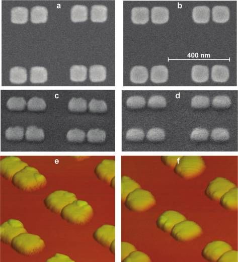
FIGURE 1. (a) Schematic of the nanoantenna unit cell (side and top
view). (b) FE-SEM image of a nanoantenna array (scale bar is 400
nm).

                                                                           FIGURE 2. Transmission spectra from the sample after different
polarization is stronger than that for the y polarization. A plot          annealing temperatures for (a) x polarization and (b) for y polariza-
of the fwhm of both polarizations’ resonance with respect                  tion. The black solid line is before annealing (i.e., at 20 °C); red
to different annealing temperatures is shown in Figure 3b.                 dashed line is after annealing at 200 °C; blue short dashed line is
                                                                           after annealing at 400 °C.
Between 100 and 325 °C, annealing changes the resonance
width for the x polarization; for the y polarization, the
resonance width is modified between 200 and 325 °C.                        TABLE 1. Comparison of the Nanoantennas before and after
                                                                           Annealing
    Our observations show that there are no substantial
                                                                                             before annealing                 after annealing
changes in the particle shape at the annealing point, 400 °C.
There is also not much difference for 500 °C, and the                                         x              y               x               y
                                                                                         polarization   polarization    polarization    polarization
particles become quasi-spherical in shape after annealing at
                                                                           λr, nm          725             645             698              638
700 °C for 2 min. This means that the swell point is between               fwhmr, nm       115.5            83.6            77.6             55.7
500 and 700 °C. According to the literature21 the grains grew              loss factor       3.53                            1.35
by a grain boundary migration but not by coalescence of the                roughness,        2.6                             1.7
                                                                             nm
grains in the range above the room temperature. Therefore                  grain size,      22                              40
the swell point is higher than the annealing temperatures                    nm

used here since coalescence starts typically at about half of
the melting temperature.                                                   the surface energy associated with the two free surfaces of
    In addition to minor changes in surface quality and                    the film becomes comparable with the surface energy of the
geometric dimensions, annealing is believed to cause sig-                  grain boundaries. As a result, grooves may develop on the
nificant internal grain growth. The process of grain growth                surface along lines where the grain boundaries meet the free
has been studied for quite some time22 and is described by                 surface. This prevents the boundaries from further migrating
grain boundary migration.21 If the grain size is small com-                and leads to grain-growth stagnation. Another possible effect
pared with the film thickness, then the grain structure and                is that differences in the free surface energy for grains with
the grain growth process are three-dimensional. As the                     different crystallographic orientation may provide a driving
grains grow to become equal to the film thickness, most                    force for the migration of the boundaries that is additional
grains traverse the entire thickness of the film, at which point           to that provided by grain boundary capillarity. Grains with

     © 2010 American Chemical Society                                918                         DOI: 10.1021/nl9037246 | Nano Lett. 2010, 10, 916-–922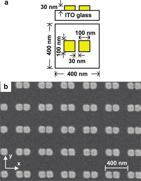
FIGURE 3. (a) Resonance wavelength and (b) resonance fwhm
changes versus annealing temperature for both polarizations.
                                                                         FIGURE 4. Experimental and simulated transmittance and reflec-
                                                                         tance spectra for (a) the original sample at room temperature and
favorable orientations (plane parallel to the surface) will grow         (b) the sample after 400 °C annealing. The black and green curves
                                                                         show the transmittance for x and y polarizations. Red and blue
at the expense of grains with unfavorable orientations. A few            curves show the reflectance for x and y polarizations. The solid lines
grains grow very large by consuming other “unfavorable”                  are experimental data, and the open circles are simulation data. The
grains. Improvement in the internal grain structure leads to             loss factor in the Drude model which is used for modeling is 3.54 in
                                                                         (a) and 1.35 in (b).
a sharper resonance as quantified by a decreased fwhm.
    More specifically, the improved grain structure results in
a decreased ε′′ ) Im (ε), obtained from eq 1. Figure 4 shows             the images, it has been determined that there is only a small
a comparison between experimental spectra and numerical                  change (∼3%) in the particle’s dimension before and after
simulations obtained by finite element method (FEM) tech-                annealing. From simulations, we know slight changes in the
niques. In fitting simulations to experiments, we use eq 1               geometric dimensions are not equivalent to a change in loss
with Drude parameters from Johnson and Christy (J&C) data7               factor, which represents the net effect of both the surface
ωp ) 9 eV and Γp ) 0.07 eV, and with two Lorentzian                      and internal structural quality of the metal. We also examine
oscillators with parameters as follows: f1 ) 0.3, ω1 ) 2.7 eV,           changes in surface quality using tilted FE-SEM and AFM
Γ1 ) 0.3 eV, f2 ) 0.8, ω2 ) 3.05 eV, Γ2 ) 0.5 eV. The loss               measurements, shown in panels c and d of Figure 5 with a
factor R is used to modify the gold damping term (Γp) to                 tilt angle of 60°. From the SEM, it can be seen that the
introduce the difference between J&C’s bulk gold dielec-                 surface roughness of the nanoantenna is smoother after
tric constant and the dielectric constant of the gold                    annealing. Panels e and f of Figure 5 show AFM 3D images.
nanoantenna. The simulation parameters used to fit the                   In Figure 5e, small bumps signify the formation of small
experimental transmission and reflection data in Figure                  polycrystalline grains. Annealing creates larger grains, lead-
4 show that the annealing treatment corresponds to a                     ing to smaller average roughness. The polycrystal grain
decrease in the loss factor of gold from 3.54 to 1.35 after              structure could be the primary reason for surface roughness.
annealing at 400 °C.                                                     In order to measure the surface roughness on the slightly
    The shape and profile of the sample before and after 400             curved surfaces of the square particle, a small area plane-fit
°C annealing are shown in panels a and b of Figure 5. From               (60 nm × 60 nm) is used before measuring roughness. The

     © 2010 American Chemical Society                              919                         DOI: 10.1021/nl9037246 | Nano Lett. 2010, 10, 916-–922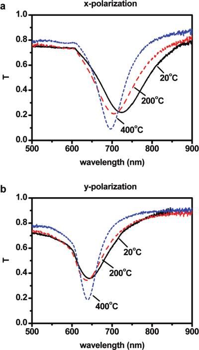
FIGURE 5. (a) SEM plane view image before annealing and (b) after
annealing (the scale bar is 400 nm). (c) Tilted SEM (incident angle
) 60°) before annealing and (d) after annealing. (e) AFM 3D image
of the sample before and (f) after annealing (the image size is 1
µm × 1 µm).
FIGURE 6. (a) An example FEM mesh of a nanoantenna pair with
rms roughness on the top of the nanoantenna is reduced roughness (top and side view). (b) The resulting transmission and
reflection spectra for the primary polarization for smooth, (5 nm,
from 2.57 to 1.73 nm after 400 °C annealing. and (10 nm bump amplitudes.
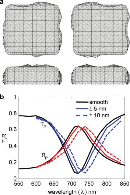
As has been discussed, surface roughness may contribute
to loss factor, resulting in decreased resonance strength and
broadening. However our simulations show that for moder- modeling loss factor after annealing are not due to surface
ate roughness, no significant changes are observed in the improvement but are primarily due to changes in internal
relaxation rate. To examine this effect, three-dimensional defects.
simulations of square-particle nanoantennas with surface The internal metal grain structure was analyzed by using
roughness are shown in Figure 6. These simulations place X-ray diffraction (XRD) measurement, where the crystal size
displacement “bumps” over the surfaces of the nanoanten- is quantified by analyzing peak broadening of the Bragg
nas, simulating roughness. Bump amplitudes of 0 nm reflections in the Cu KR X-ray diffraction scans as taken in
(smooth), (5 nm, and (10 nm have shown that increased the θ/2θ mode. The grain size (dg) is determined from
surface roughness may shift the resonance wavelength but the (111) reflections using the standard Debye-Scherrer
does not significantly influence the loss factor. Note that formulation.23
roughness in the gaps may provide a significant contribution
to the inhomogeneous broadening of a plasmon resonance.
Kλ
The effect of the gap size diversity was analyzed using average crystallite size (dg) ) (2)
Bstruc cos θ
representative nanoantennas similar those presented in
panels a and b of Figure 5. One can see from Figure 5 and
also more detail consideration shows that the roughness in
the gap is less than 5 nm (Rrms measurements from panels In eq 2 K describes the crystallite shape factor, λ is X-ray
a and b of Figure 5 in the gap are 2.5 nm before annealing wavelength, and θ describes the angle of incidence. For our
and 2.4 nm after annealing) which means that the broaden- measurements K is taken to be 0.9, which is typical for
ing is actually less than that simulated in Figure 6b with the spherical grains (K is in a range from 0.8 to 1 for possible
solid blue line and can be estimated as about 2 nm, which variations in shape), λ is 0.514 nm for the copper anode.
is indeed not a significant contribution to the broadening. Bstrucdescribes the structural broadening, which is the differ-
Therefore, we may conclude that significant changes in ence in the integral profile width as defined in eq 3
© 2010 American Chemical Society 920 DOI: 10.1021/nl9037246 | Nano Lett. 2010, 10, 916-–922
Bstruc ) √Bobs2 - Bstd2               (3)

where Bobs is the full-width measured at half-maximum
intensity of the sample and Bstd equals 0.19° as measured
for an Au(111) single-crystal standard.24
    Figure 7 shows the XRD θ/2θ measurement of the
nanoantenna sample before and after annealing. The Au(111)
diffraction angles for both samples are 38.2° for the θ/2θ
measurement. Bobs of the original nanoantenna sample is
0.416° and Bobs of the annealed nanoantenna sample is
0.283°. Using eq 2, we may calculate that the average grain
size has increased from 22 to 40 nm.
    Note that the Debye-Scherrer formula implies just one,              FIGURE 7. XRD θ/2θ measurement of the nanoantenna before
                                                                        (black) and after (red) annealing.
“average” size of the grains for any grain shape. This means
that if the formula gives a grain size of 40 nm, larger than
                                                                        TABLE 2. Comparison of the Electron Collision Rate and Grain
the thickness (31 nm after annealing), one can expect a                 Size for Nanoantennas, J&C,7 and Motulevich’s Data12
slightly larger than 40 nm size in the x-y plane.
                                                                                  before annealing    after annealing       J&C     Motulevich
    In order to analyze the electron relaxation rate we use a
                                                                        Γg, meV       241                  93             72            30
quantitative model based on the linearized Boltzmann equa-              D, nm          22                  40             50           200
tion.11 In this model, grain boundaries are represented as N            R               0.78                0.67           0.64          0.39
parallel partially reflecting planes, located perpendicular to
the electric field E, and placed an average random distance
                                                                        surements where the contribution of grain size was deter-
d apart. Mathematically, these planes are identified with
                                                                        mined. Data obtained by Motulevich for gold films is sup-
scattering potentials of height U (energy) and width w
                                                                        ported by grain contribution and grain size measurements.12
(actually delta functions of strength S ) Uw); inside the
                                                                        Reference relaxation rate was determined from Fres/F ) ved/
grains, the electron scattering is described by a relaxation
                                                                        (vep + ved), where the residual resistance Fres was measured
time τ. If d is identified with the average grain diameter D,
                                                                        at 4.2 K. The data by Motulevich show that the electron
the model gives total relaxation time in the metal with
                                                                        relaxation rate for infinite grain size is caused by electron-
grains, τg
                                                                        phonon collision rate τ0-1 ) Γ0 ) Γep ) 26 meV and grain
                                                                        contribution Γed ) 4 meV with grain size about 200 nm.
         τg                                                                The grain boundary reflection coefficient, R is often taken
            ) 1 - 1.5 + 32 - 33 ln(1 + -1)             (4)
         τ                                                              to be 0.5 as a first approximation.25 One can see however
                                                                        from our data (Table 2) that the reflection coefficient can be
                                                                        different for nanoantennas before and after annealing likely
where                                                                   due to a different volume fraction for the grain boundaries
                                νFτ R                                   and, consequently, the strength of the scattering potentials.
                          )                                            We should note that the difference in reflection coefficients
                                 D 1-R                                  between 0.7 and 0.8 makes a large difference in the relax-
with the electron reflection coefficient, R, introduced from            ation rate for the same grain size, which is about 100 meV
the potential barrier strength as R/(1 - R) ) S2/p2, and vF )           at 22 nm and much larger than the experimental error in
1.35 × 10⁶ m/s is the Fermi velocity for Au.                            the relaxation rate measurements.
   The solution for inverse of the relaxation time (τg-1 ) Γg)
                                                                           To summarize, annealing not only increases the metal
can be approximated by simple linear dependence on the
                                                                        grain size but also reduces the reflection coefficient of the
inverse grain size D-1
                                                                        potential barriers. Both factors result in a substantially
                                                                        improved electron relaxation rate for nanostructures, leading
                                        1.37vFR                         to a value comparable with large area samples. The grain
                   τg-1 ) τ0-1 +                           (5)
                                        D(1 - R)                        contribution to the electron relaxation rate is reduced by a
                                                                        factor of 3.2 due to the grain size being increased from 22
                                                                        to 40 nm. Additionally the reflection coefficient has been
   In this equation τ0 is the relaxation time of infinite grain         reduced from 0.78 to 0.67.
size. A choice of the reference relaxation rate for an infinite            Note that loss due to internal grains also explains our
grain size requires special discussion. Careful consideration           previous results for size-dependent permittivity with a large
of possible sources show that there are not so many mea-                A-factor (the coefficient in the size dependence) and the

     © 2010 American Chemical Society                             921                       DOI: 10.1021/nl9037246 | Nano Lett. 2010, 10, 916-–922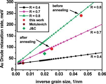
for silver is about 103 °C lower than that for gold, 961 °C
                                                                             versus 1064 °C). Significant narrowing of the plasmon
                                                                             resonance has been observed for silver nanoantennas as
                                                                             well.
                                                                                Indeed the result of annealing shows a complex depen-
                                                                             dence on particle size, aspect ratio, and material. Therefore,
                                                                             optimal annealing conditions for specific sample types must
                                                                             be tailored to the individual parameters of the sample.

                                                                               Acknowledgment. This work was supported in part by
                                                                             U.S. Army Research Office under Grants 50372-CH-MUR and
                                                                             50342-PH-MUR.

                                                                             REFERENCES AND NOTES
FIGURE 8. Au electron scattering rate, Γg (Γ0 ) 26 meV) calculated           (1)    Su, K. H.; Wei, Q. H.; Zhang, X.; Mock, J. J.; Smith, D. R.; Schultz,
with the above model at R ) 0.4, 0.7, and 0.8. The results for gold                 S. Nano Lett. 2003, 3, 1087–1090.
nanoantennas were plotted with red circles. The Motulevich result            (2)    Sundaramurthy, A.; Schuck, P. J.; Conley, N. R.; Fromm, D. P.;
for gold is shown with a brown circle, while the Johnson and Christy                Kino, G. S.; Moerner, W. E. Nano Lett. 2006, 6, 355–360.
result is depicted with a green diamond. The grain size is taken             (3)    Kim, S.; Jin, J. H.; Kim, Y. J.; Park, I. Y.; Kim, Y.; Kim, S. W. Nature
approximately equal to film thickness, 50 nm in the J&C7 case.                      2008, 453, 757–760.
                                                                             (4)    Bakker, R. M.; Yuan, H. K.; Liu, Z. T.; Drachev, V. P.; Kildishev,
                                                         14
                                                                                    A. V.; Shalaev, V. M.; Pedersen, R. H.; Gresillon, S.; Boltasseva,
observed independence on the surface roughness. Indeed                              A. Appl. Phys. Lett. 2008, 92, No. 043101.
the large A-factor indicates that the grain size is more crucial             (5)    Bakker, R. M.; Drachev, V. P.; Liu, Z. T.; Yuan, H. K.; Pedersen,
                                                                                    R. H.; Boltasseva, A.; Chen, J. J.; Irudayaraj, J.; Kildishev, A. V.;
than structure size. Also, the electron scattering at the grain                     Shalaev, V. M. New J. Phys. 2008, 10, 125022.
boundaries would significantly affect the electron relaxation                (6)    Gupta, R.; Dyer, M. J.; Weimer, W. A. J. Appl. Phys. 2002, 92,
rate, more than that by surface roughness of the entire                             5264–5271.
                                                                             (7)    Johnson, P. B.; Christy, R. W. Phys. Rev. B 1972, 6, 4370–4379.
particle. The restructuring increases grain size and decreases
                                                                             (8)    Homola, J.; Yee, S. S.; Gauglitz, G. Sens. Actuators, B 1999, 54,
the internal boundary reflection coefficient, both of which                         3–15.
substantially improve the quality of the plasmon resonance.                  (9)    Huang, W. Y.; Qian, W.; El-Sayed, M. A.; Ding, Y.; Wang, Z. L. J.
                                                                                    Phys. Chem. C 2007, 111, 10751–10757.
    Finally we qualitatively discuss whether the above results
                                                                             (10)   Kuttge, M.; Vesseur, E. J. R.; Verhoeven, J.; Lezec, H. J.; Atwater,
may be applied to nanostructures of different shape, size,                          H. A.; Polman, A. Appl. Phys. Lett. 2008, 93, 113110.
and material (silver). Although annealing is shown to greatly                (11)   Mayadas, A. F.; Shatzkes, M.; Janak, J. F. Appl. Phys. Lett. 1969,
improve the quality of gold nanoantennas by decreasing the                          14, 345–347.
                                                                             (12)   Motulevich, G. P. Optical properties of metals; Skobel’tsyn, D. V.,
electron relaxation rate, and similar results have been                             Ed.; Consultants Bureau: New York, 1973.
obtained for silver nanoantennas, some types of structures                   (13)   Weber, M. J. Handbook of optical materials; CRC Press: Boca
may not benefit from annealing, as discussed in the intro-                          Raton, FL, 2003.
                                                                             (14)   Drachev, V. P.; Chettiar, U. K.; Kildishev, A. V.; Yuan, H. K.; Cai,
duction. Heating initiates the Rayleigh instability and brakes                      W. S.; Shalaev, V. M. Opt. Express 2008, 16, 1186–1195.
strips into isolated particles. As with any instability the result           (15)   Kaiser, N. Appl. Opt. 2002, 41, 3053–3060.
depends on the initial conditions and driving forces; in the                 (16)   Kreibig, U. J. Phys. F: Met. Phys. 1974, 4, 999–1014.
                                                                             (17)   Hulteen, J. C.; Patrissi, C. J.; Miner, D. L.; Crosthwait, E. R.;
case of the strips, it depends on the width and initial quality                     Oberhauser, E. B.; Martin, C. R. J. Phys. Chem. B 1997, 101, 7727–
of the gold. We also found that the absolute value of the                           7731.
dimensions is more important than aspect ratio; for example                  (18)   Habenicht, A.; Olapinski, M.; Burmeister, F.; Leiderer, P.; Boneberg,
                                                                                    J. Science 2005, 309, 2043–2045.
annealing does not improve quality in the case of 50 × 100                   (19)   Huang, W.; El-Sayed, M. A. Eur. Phys. J.-Spec. Topics 2008, 153,
× 30 nm but does work for 100 × 200 × 30 nm. The gap                                223–230.
dependence was studied for gold nanoantennas of a square                     (20)   Zheng, Y. B.; Huang, T. J.; Desai, A. Y.; Wang, S. J.; Tan, L. K.;
                                                                                    Gao, H.; Huan, A. C. H. Appl. Phys. Lett. 2007, 90, 183117.
shape. The positive results are almost independent of the                    (21)   Yoshida, N.; Oshima, R.; Fujita, F. E. J. Phys. F: Met. Phys. 1972,
gap size. Moreover if one takes slightly touching particles,                        2, 237–246.
they will separate during annealing at 400 °C, and it is                     (22)   Feltham, P. Acta Metall. 1957, 5, 97–105.
                                                                             (23)   Chen, G.; Hui, P.; Pita, K.; Hing, P.; Kong, L. Appl. Phys. A: Mater.
possible to obtain nanoantennas with a very narrow gap.                             Sci. Process. 2005, 80, 659–665.
    Annealing can be applied to silver nanoantennas, but at                  (24)   Jankowski, A. F.; Saw, C. K.; Harper, J. F.; Vallier, B. F.; Ferreira,
lower temperatures, about 250 °C (lower temperature is                              J. L.; Hayes, J. P. Thin Solid Films 2006, 494, 268–273.
                                                                             (25)   Marsillac, S.; Barreau, N.; Khatri, H.; Li, J.; Sainju, D.; Parikh, A.;
expected; all the restructurings happen at the temperature                          Podraza, N. J.; Collins, R. W. Phys. Status Solidi C 2008, 5, 1244–
which is a fraction of melting temperature; the melting point                       1248.

     © 2010 American Chemical Society                                  922                            DOI: 10.1021/nl9037246 | Nano Lett. 2010, 10, 916-–922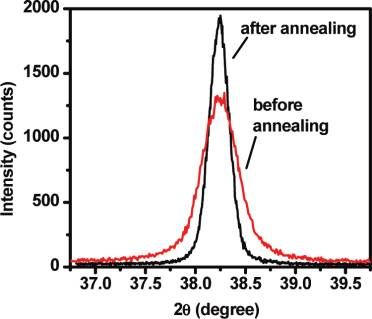
You can also read


