Module Design and Assembly - Adam Anderson, Greg Derylo (FNAL), + many module and readout experts CMB-S4 Collaboration Meeting 11 March 2021
←
→
Page content transcription
If your browser does not render page correctly, please read the page content below
Module Design and
Assembly

Adam Anderson, Greg Derylo (FNAL), + many module and readout experts
CMB-S4 Collaboration Meeting
11 March 2021
                                    1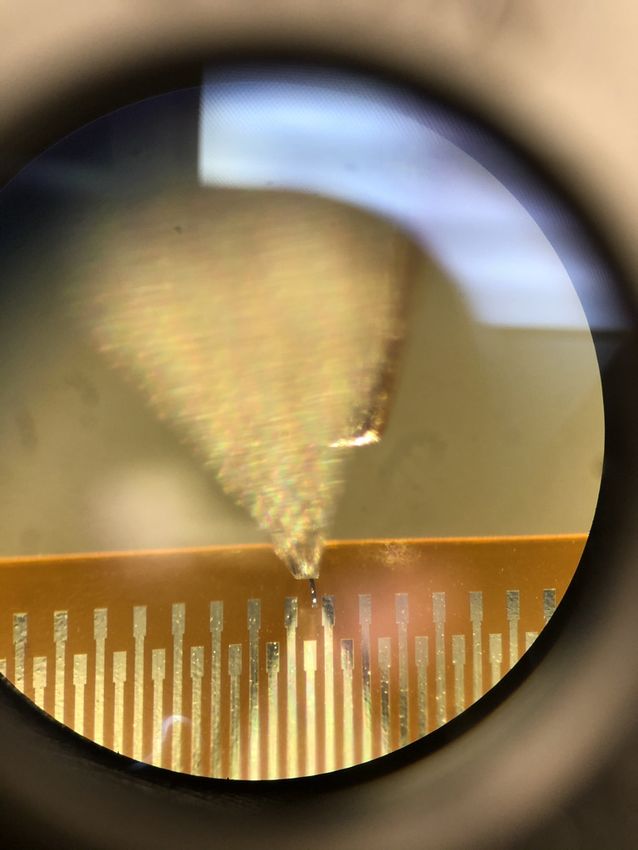
High-Level Overview
• Early design work identi ed several areas requiring additional
     R&D in order to satisfy existing system interface requirements
     (e.g. requirement of superconducting ex cables, module pitch in
     SATs)

• Does not make sense for early (“CDFG”) detector testing to
     depend on outcomes of R&D for production modules

• To enable early integrated tests of CDFG detectors + some
     readout, we are forking the module design:

     • “CDFG module” - Simple design using shovel-ready hardware
       that ts in the cryostats identi ed for CDFG testing (FNAL,
       Illinois, SLAC)

     • Production module - Module that we will actually deploy,
       satisfying all project interface requirements
                                          2
fi
                      fi
                            fi
                                     fl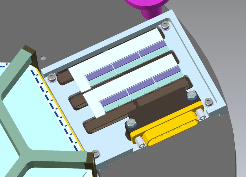
Module R&D Areas
• Superconducting ex cables are required by readout/module interface
      • Limit of conventional ex PCB fab (e.g. TechEtch) is around ~9mils pitch; need
        4mils pitch; other processes have higher resolution, but higher cost and limited
        vendors

• SAT module pitch of 124mm
      • Forces ex cables on top of backshort with step bond, which complicates
        mounting and requires wire bonding R&D

      • Limits mechanical space in ways that require some study: less room for magnetic
        shielding (low-f noise risk) and focal-plane mounting structure (vibrational risk)

• Readout density and assembly
      • Packaging readout for SAT HF (1876 detectors) requires signi cant area of
        readout electronics

      • Challenging to t these behind the detector wafer footprint in a way that can be
        bonded and assembled without elaborate origami

                                               3
 fl
            fi
                 fl
                      fl
                                                            fi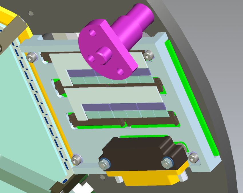
CDFG Testing Module
• See speci cations document
• Planar layout a la AdvACT to relax constraint on ex cable
• Use only 2 columns of readout per side of wafer to enable
  compatibility between SAT and LAT wafer pinouts

• Diameter of footprint needs to be
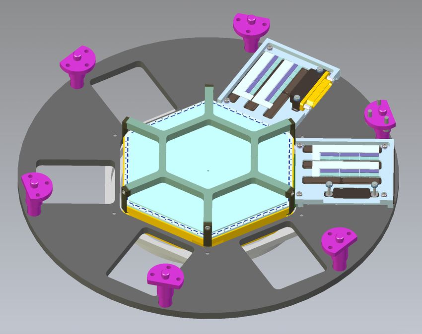
Mounting in LD400 Cryostat
                       Ports for access to
                       ZIF connectors on
                        back of readout
                             boards

                       diameter = 270mm

                           mounting ring
                         (adapt to unique
                         feedthroughs of
                          test cryostats)

                        mixing chamber
                             stage

               5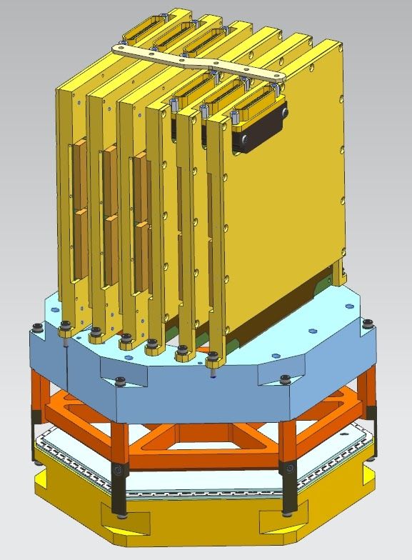
Back View
                     Readout columns
                     (width = 15mm each)

                     Mounting ring to
                     clamp wafer stack
                     (BeCu or brass
                     springs not shown)

                     Compatible with
                     direct bonding and
                     short ex cable
                     between readout and
                     wafer

                     Readout boxes (PCB
                     not shown)

                 6
fl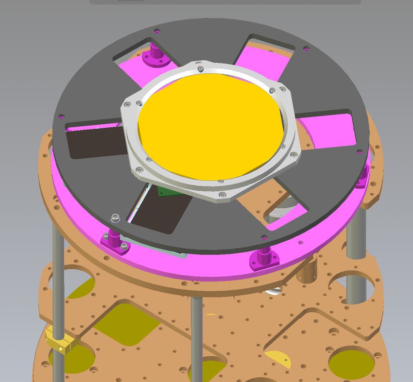
CDFG Module Next Steps
• Final iteration on readout box design with readout working group
      (G. Haller, Z. Ahmed)

• Quantify minimum magnetic shielding needed for TDM readout in
      test cryostat con guration

• Simple simulations of magnetic eld suppression in SLAC,
      Illinois, FNAL test cryostats to verify that we meet shielding spec

• Tweak mounting to avoid collisions with wiring feedthroughs,
      other xtures, in test cryostats

                                        7
 fi
                fi
                                fi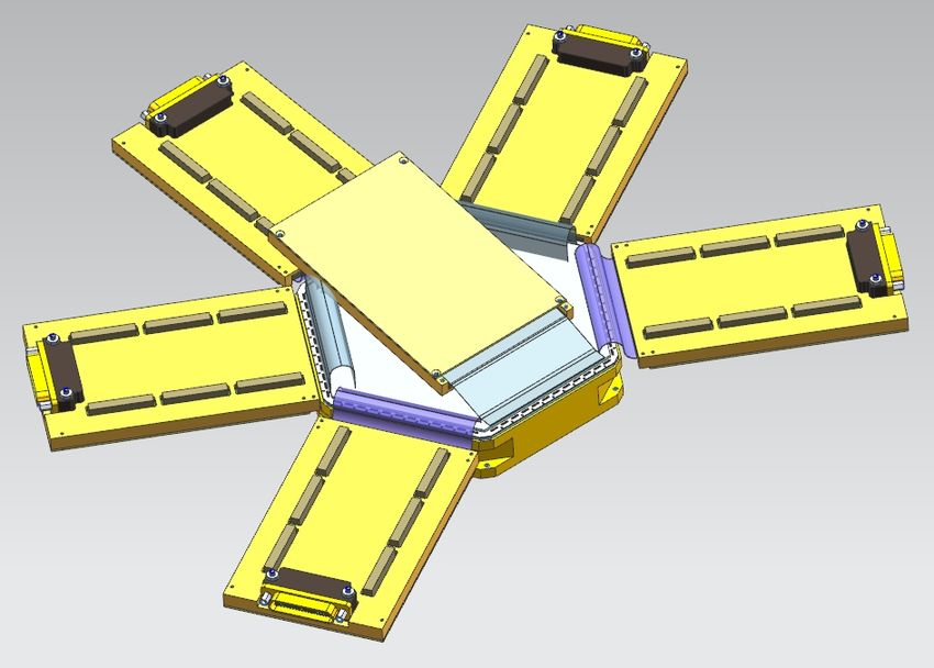
Production Module - v1
                             • First module concept that
                               met key interface
                               requirements
                   m m
                90           • 90-mm width readout boxes
                               on back, barely t behind
                               wafer footprint

                             • Flex cable (not shown)
                               requires complicated routing
                               from edge of wafer to box,
                               with 60deg bend

                             • Long cables are di cult to
                               assemble and fabricate, put
                               pressure on inductance
                               budget
                         8
     fi
          ffi
Readout Boxes - v2 in progress
                                  residual collisions                         • Achieved signi cant reduction
                                                                                in box width with denser wiring
                                                                                chips, corrected MUX chip
                                                                                dimensions (90mm -> 65mm)

                                                                              • Flex cables drastically
                                                                                shortened, eliminated twisting/
                                                                                routing problem
     ZIF connectors for
     row selects (must                                                        • Final layout/dimensions of
       be right-angle)                                                          readout box pending nal
                                                                                MUX column wiring chip
                                                                                con guration (see G. Haller
                                                                                readout talk)
                                                          a t c h d etector
                          NB: readout mounting          m             dth
                                                          edge wi
                            plate not shown                                   • Residual collisions in corners,
                                                                                resolve with some combination
                                                                                of ne-tuning box width,
                                                                                removing material, and
                                                                                “pinwheel” orientation

                                      m m ed   ge                             • Include springs on readout
                               63 . 4                                           mounting plate as on previous
                                                                                slide

                                                           9
fi
     fi
                fi
                          fi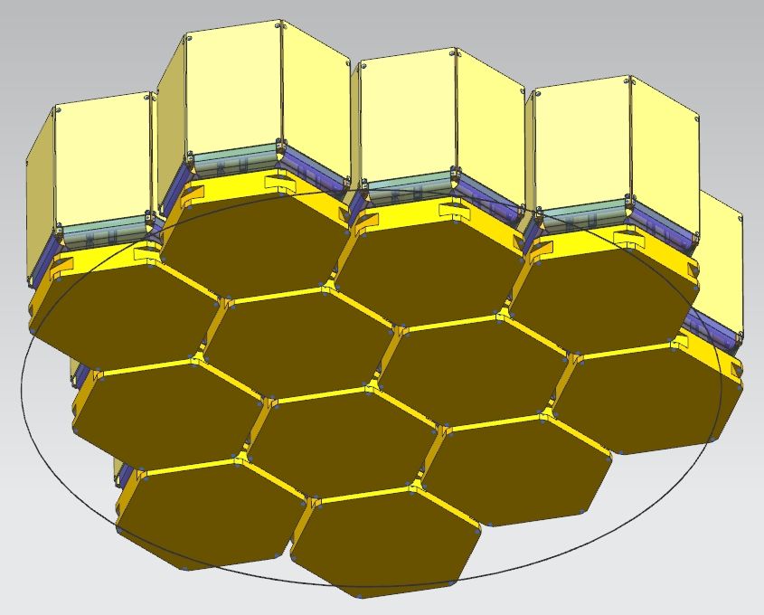
SAT Focal Plane Configuration

                                                           Pitch s
                                                                   hown:
                                                             127mm

                                           Horn
                                                at-to-
                                             120.8m at:
                                                    m

                                                                 SAT target pitch of 124mm
                                                                 leaves only 3.2mm of gap
           mu-metal sleeve or Nb cup would                          between horn arrays
          need to t between footprint (see A.         10
           Schillaci, L. Moncelsi readout talk)
fl
     fi
             fl
SAT Pitch Problem
Important radial distances: • In current design, there is 1.6mm or
0.7mm clearance for focal plane plate
+ magnetic shield, modulo precise
locations. Seems inadequate.
3.2mm… this seems large • Possible solutions:
backshort wafer: 56.2mm
• Relax 124mm pitch: reduces SAT
mapping speed.
detector+interface wafers: 59.4mm • Shrink detector+interface wafers
and horn array, holding backshort
and horn array by ~2mm. No impact
corner bracket: 61.3mm
to optics. Reduces area for
bondpads and mechanical support
allowable envelope: 62.0mm of outer horn wall.
• Eliminate focal plane plate, and
expand horn arrays to bolt directly
horn array: 60.4mm into each other. Probably too
radical, but arguably not insane.
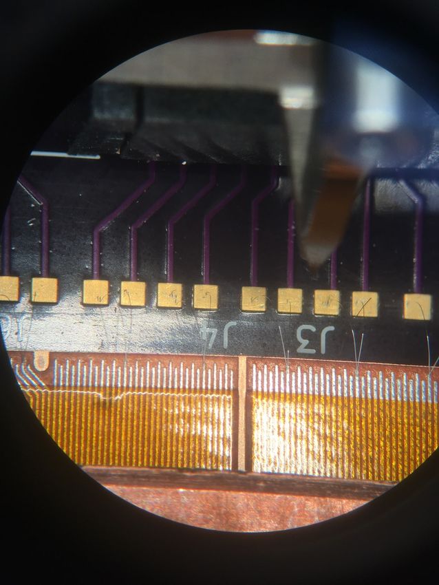
extent of horns: ~56mm 11Assembly
• Because of SAT pitch
requirement, ex cables must
mount inward (detector wafer
is 119mm and pitch is
124mm)
• In order to maintain bondpads
on same side of ex cable at
both ends, box must fold
back into backshort during
bonding
wire bonding head in
Fermilab machine • Jig needed to hold boxes
during bonding steps
• Head of Fermilab wire
bonding machine is non-trivial
in size—critical to include in
3D model of assembly
12
fl
flpitch R
Flex Cables
Vendor / heritage Stack Ic Cost
(trace/space) (T=100mK)
7-10 mOhm
polyimide / (~4 inches) No SC
TechEtch / 9um tinned Cu 2mils / 2mils (expect transition ~$250
SPT-3G / polyimide 50mOhm for observed
• Superconducting ex cables are key RRR~100)
R&D problem; no extant solution polyimide /
meets volume, cost, and trace TechEtch / 50-300uinches
2mils / 2mils
Cooling Cooling
~$250
PB2a tinned Cu / down down
density requirements polyimide
polyimide /
TechEtch / 4.5mils / Bonded, in Bonded, in
• Considered two options: SPIDER
aluminum /
polyimide
4.5mils queue queue
~$250
Flexible Circuits polyimide /
1. Superconducting aluminum, 1 mil Al / 4mils / 4mils fab failed fab failed ~$250
2mils/2mils trace/space (1- Technology polyimide
layer) or 4mils/4mils trace/ SLAC polyimide / Al 90um TBD TBD TBD
space (2-layer)
TechEtch claims yield drops signi cantly atNext Steps
• CDFG test module is straightforward and will proceed in tandem
with readout layout
• Production module with readout boxes parallel to each side of
hex (v2) is probably viable
• Need to nalize readout box mechanical design together with
readout layout
• Flex cables remain a major R&D task
• Further study and implementation of magnetic shielding
14
fiBackup
15Readout Box Detail
Exact positioning of chips 6x 45-position ZIF
relative to wafer is subject to connectors on
iteration during layout of backside of PCB
carrier PCB
Constrained PCB
footprint doesn’t
allow much space for
magnetic shielding of
the carrier… needs
to spec allowable B-
eld for lab testing
16
fiMagnetic Shielding Considerations
Accommodation for
sheet of mu-metal
for magnetic
shielding; annular
ring also possible
Level of detail in
magnetic shielding
strategy for readout
in CDFG test module
is extremely
primitive. Further
development and
basic simulations
needed.
17Production Module - Key Interfaces and Requirements
• Readout:
• MUX chips should be housed in modular boxes, necessitating use of superconducting ex
cables
• Need to control inductance in superconducting wiring to TES (needs spec)
• Detectors:
• 118.8mm wafer size (hex side-to-side); inherited from SO
• SAT:
• 124mm wafer pitch (hex side-to-side); allows 2.6mm between edge of silicon and boundary of
hex footprint
• Accommodations for mounting in a curved focal plane (new this week)
• Modules and assembly:
• Assembly and wire bonding must be physically possible
• High-yield assembly must take 1 technician-day
Module design is highly sensitive to interface mechanical dimensions. Changes
of ~1mm can make or break design con gurations.
18
fi
flYou can also read