Multi Gigabit Wireless Data Transfer for High Energy Physics Applications - Indico
←
→
Page content transcription
If your browser does not render page correctly, please read the page content below
Multi‐Gigabit Wireless Data
               Transfer for High Energy Physics
                         Applications

www.cea.fr

    &        cedric.dehos@cea.fr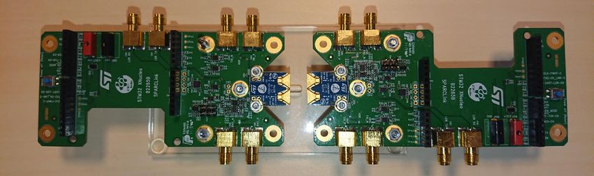
Outline
         Cliquez pour modifier le style du titre

Introduction to millimeter wave, focus on 60GHz

RF integrated circuit architecture and design

Antenna requirement, design and integration

Feasibility tests for HEP

Technology roadmap

&                            © CEA. All rights reserved   |2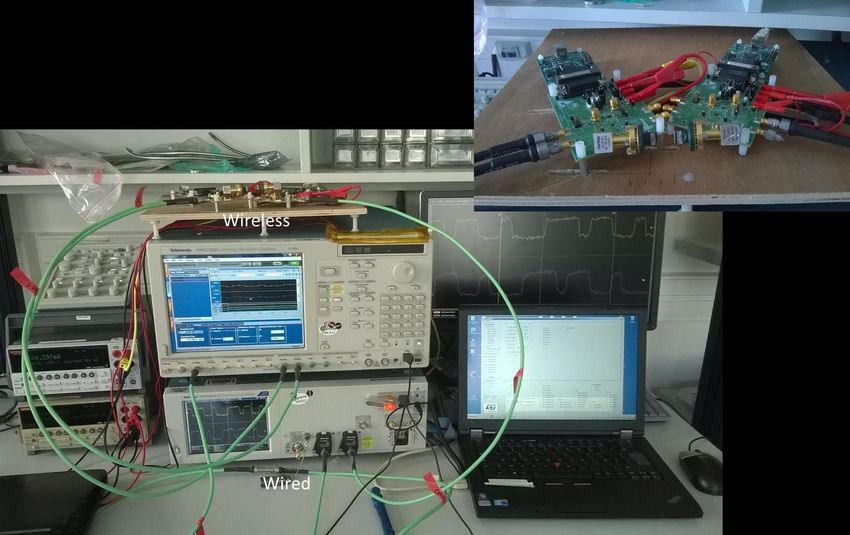
Cliquez pour modifier le style du titre

     Introduction to millimeter wave,
             focus on 60GHz

    CONTEXT AND MOTIVATION

&                      © CEA. All rights reserved   |3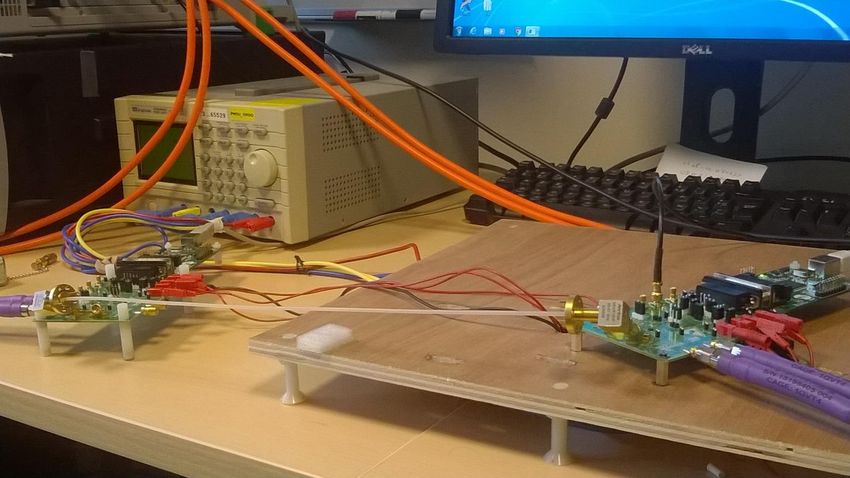
Introduction to millimeter wave
    Cliquez pour modifier le style du titre

&                   © CEA. All rights reserved   |4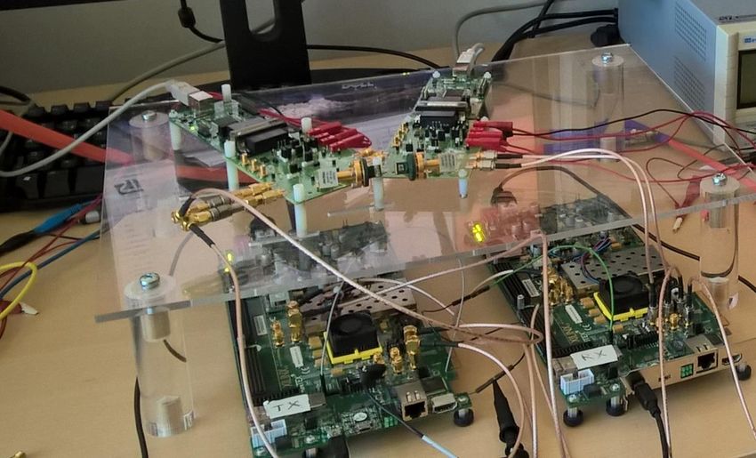
Introduction to millimeter wave
Cliquez pour modifier le style du titre
Definition
1-10mm wavelength
30-300GHz carrier frequency
MmW rationale
Short wavelength
High level of integration, compact antenna scheme
High free path loss
Suitable for short range 60GHz system in package
with integrated antenna
High frequency reuse
Huge available bandwidths for high data rate communication
14GHz in V Band, 35GHz in D Band
Natural immunity to interference
& © CEA. All rights reserved |5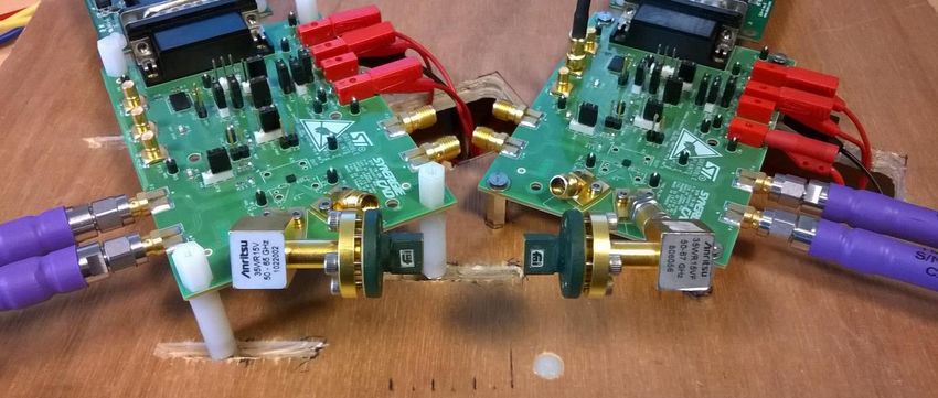
Introduction to millimeter wave
                 Cliquez pour modifier le style du titre
        Millimeter wave current applications
          Radio astronomy

          Military and space

          Cellular Infrastructure, 5G small cell
R
          Automotive Radar
A
N
          Wireless HD
G
E         WLAN 802.11ad, 802.11ay

          Imaging and security

          Short range, chip to chip,
          contactless connectivity
    &                                              © CEA. All rights reserved   |6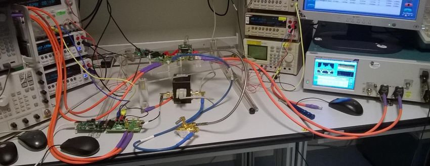
Features of the 60GHz band
Cliquez pour modifier le style du titre
Huge worldwide unlicensed channels
FCC extension : 64-71GHz
WRC19: 57-71GHz identified to enable 5G deployment (IMT 2020)
Favorable regulation for short range device
Low maximum transmit power : 10dBm (Europe-Japan)
FCC
emission limit for UWB systems: -51.3 dBm for indoor at 3m
40-200GHz spurious emissions: -10 dBm EIRP max at 3m
ETSI
9GHz occupied bandwidth
Unwanted emissions (frequencies beyond the limit of 250 % of the necessary
bandwidth) in the spurious domain: -30dBm (in operating mode ) and -47dBm (in
standbye mode)
& © CEA. All rights reserved |7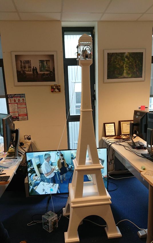
Features of the 60GHz band
           Cliquez pour modifier le style du titre
Short (5mm) wave length
     High free space loss:
     28dB@1cm; 48dB@10cm; 68dB@1m
     Small antenna size
     System in package integration
                                      6,5*6,5mm² 60GHz SiP
                                       2.5mm patch antenna

Compatible with low cost CMOS
     Design at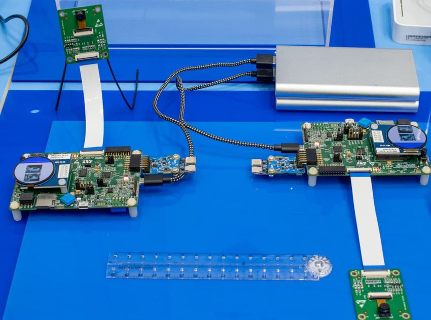
Zigbee

               Features of the 60GHz band
         Cliquez pour modifier le style du titre                  Bluetooth LE

    Is mmw low power ?

                                                   MIMO Beam
                                                   Forming

                         Digital Base Band

&                           © CEA. All rights reserved                           |9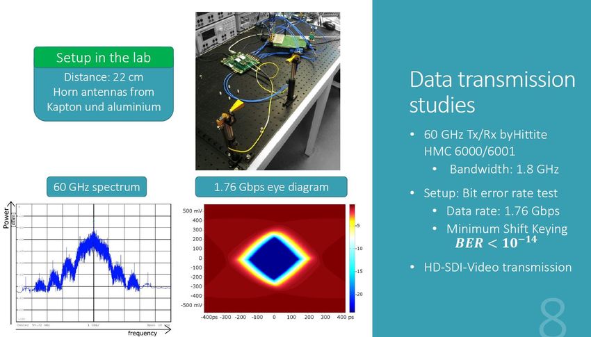
Cliquez pour modifier le style du titre

    RF integrated circuit architecture and design

        CONTEXT AND MOTIVATION

&                            © CEA. All rights reserved   | 10
RFIC architectures
Cliquez pour modifier le style du titre
Coherent architecture
- Up to 6 bit/Hz
- >100pJ/bit
Non coherent architecture (On/Off keying)
-RFIC architectures
Cliquez pour modifier le style du titre
Coherent architecture
Widely used today as the most efficient (range, robustness, and
spectral efficiency)
Need power hungry PLL and digital base band processor
Signal processing latencies
Performance metrics: EVM, SNR, BER, PER
Non coherent architecture (On/Off Keying)
Former and simple analog technology
Very low power, almost no latency
Ideal for cable replacement at short range
Weak sensitivity (short range) and spectral efficiency
Sensitive to multi paths, interferers
Performance metrics: eye diagram, jitter, BER, PER
& © CEA. All rights reserved | 1260GHz RFIC design
Cliquez pour modifier le style du titre
60GHz contactless connector (2011-2015)
Technology:
- 60GHz OOK transceiver in CMOS SOI 65nm
- Super-regeneration receiver
- Integrated antennas
Demonstrated performances:
- HD Video streaming
- Data rate: up to 2.5Gbps
- Range: 10cm
- Power consumption: 50mW (20pJ/bit)
& © CEA. All rights reserved | 1360GHz RFIC design
Cliquez pour modifier le style du titre
60GHz contactless connector (2015-2017)
Technology:
- 60GHz ASK transceiver in CMOS 65nm
- Non coherent receiver (envelop detector)
- BGA package
- External antennas
Demonstrated performances:
- HD Video streaming (2Gbps FPGA limited)
- Data rate: up to 6Gbps
- Range: 3cm with 4dB gain antenna
- Power consumption: 35mW (60GHz RFIC design
Cliquez pour modifier le style du titre
ST60 A2 (2019)
Technical features (from datasheet)
From 1 Mbit/s up to 6 Gbit/s data rate
RF transceiver operating in half-duplex mode
Low-power ASK modulation scheme supported
Differential SLVS input-output port (NRZ) or single-ended CMOS 1.8 V bidirectional
data for low data rate (1-100 Mbit/s with 15 pF PCB load)
24 dB typical total link budget
Supply voltage: power-optimized dual 1.8 V and 1.45 V supply or single-supply 1.8 V
Low power consumption (typical values with dual power supplies):
40 mW in half-duplex, TX mode
25 mW in half-duplex, RX mode
1.2 mW in idle mode
1.3 μW in off mode
6.6 pJ/bit for TX and 4.1 pJ/bit for RX at maximum data-rate
50 Ω single-ended nominal RF input/output impedance
Package: VFBGA 2.2 mm x 2.2 mm x 1.0 mm, 25 balls, F5x5, 0.4 mm pitch
& © CEA. All rights reserved | 1560GHz RFIC design
Cliquez pour modifier le style du titre
ST60 Application Board
High data rate differential I/Os
Low data rate single I/Os
1.8V power supply
Possible interfacing with STM32
& © CEA. All rights reserved | 1660GHz RFIC design
Cliquez pour modifier le style du titre
Ethernet demo Board
Full duplex video recording
2 chips and cross polar antenna
& © CEA. All rights reserved | 1760GHz RFIC design
Cliquez pour modifier le style du titre
ST60 A3 (2020) and roadmap
& © CEA. All rights reserved | 1860GHz RFIC design (Heidelberg)
Cliquez pour modifier le style du titre
60GHz transceiver design ongoing,
dedicated to wireless readout
Specifications in line with the HEP applications
Technology and architecture chosen from in-
depth studies
SiGe HBT BiCMOS technology
Comprehensive simulations
on the RF blocks over PVT,
mismatchs and coupling effects
Strong attention paid to
robustness and reliability
Chip under development
& © CEA. All rights reserved | 19Cliquez pour modifier le style du titre
Antenna requirement, design and integration
CONTEXT AND MOTIVATION
& © CEA. All rights reserved | 20Antenna requirement (e. g.)
Cliquez pour modifier le style du titre
Non-coherent architectureAntenna design – on Board
Cliquez pour modifier le style du titre
Antenna on Board (PCB)
Vertical and horizontal polarization available
Dimensions: 8.25 x 7.4 x 3.4 mm
Frequency band: 57 – 66 GHz
Directivity: higher than 8 dBi
ROHS and REACH compliant
& © CEA. All rights reserved | 22Antenna design – SiP
Cliquez pour modifier le style du titre
On High Resistivity Silicon (SOI HR) antenna HR SOI 65nm OOK TRX
1,9*3,1mm²
5dB antenna gain
20% bandwidth
Sensitive to wire bonding
System in Package with antennas
Transceiver flip-chipped close to the antennas
Ceramic, silicon or organic interposer
2D or 3D interconnections LCP Si
5-8dB gain HTCC 10*10mm² 6.5*6.5mm²
13.5*8.5mm²
& © CEA. All rights reserved | 23Antenna design – SiP + lens
Cliquez pour modifier le style du titre
In-Package coupled antenna and dielectric lens:
• Polyimide dielectric lens
• +8 dB antenna gain improvement
• At 2Gbps: from 6cm range to 40cm range using an external lens
• Chip size: 2x3.3 mm2; package 7x7 mm2; lens 10 mm
& © CEA. All rights reserved | 24Antenna design – SiP + lens
Cliquez pour modifier le style du titre
In-Package coupled antenna and focusing lens:
Transmit array quasi-optical lens
No mmW interconnection; +15 dB antenna gain improvement; fixed beam
At 2Gbps: from 6cm range to 190cm range using an external lens
Chip size: 2x3.3 mm2; package 7x7 mm2; lens 25x25 mm2
Discrete lens: ~16 dBi
In-package antenna : ~5 dBi
RFIC
PCB
T/R chip y
z x
OTA Measurement
& © CEA. All rights reserved | 25Antenna design
Cliquez pour modifier le style du titre
Phased array antenna with beamforming capability
Require controllable phase shifters to steer the beam
Single beam or multi-beams
& © CEA. All rights reserved | 26Antenna design
Cliquez pour modifier le style du titre
RF Beamforming approaches
Compact monochip
Fixed beam antenna array TRX and phase shifters Satellite phase shifters
PS PS
TRX TRX TRX
PS PS
80
80 70
60 60
60
40 50
Gain (dB)
40
Gain (dB)
Gain (dB)
40
20 20 30
0 20
0
1 2 4 8 16 32 64 128 256 512 1 2 4 8 16 32 64 128 256 512 10
-20 -20 0
-40 -40 -10 1 2 4 8 16 32 64 128 256 512
Number of antennas Number of antennas Number of antennas
max array factor (dB) splitter loss (dB) max array factor (dB) routing loss (dB) max array factor (dB) routing loss (dB)
routing loss (dB) total gain (dB) total gain (dB) total gain (dB)
& © CEA. All rights reserved | 27Antenna design
Cliquez pour modifier le style du titre
Beamforming with satellite phase shifter (2015)
2*4 antenna array, 17dBi gain, 36dBm EIRP
{PA, LNA, phase shifter} circuit in BICMOS55nm
Compensation of the power splitter and phase shifter losses
Vector modulator phase shifter
3D multi-layer organic module (LCP), 20*20mm²
LCP interposer module layout
60GHz transceiver
4 channels 57-66GHz
2 mm
3.4 mm
Tx/Rx switch PA, LNA, phase shifter IC
& © CEA. All rights reserved | 28Range extension using plastic waveguide
Cliquez pour modifier le style du titre
Interfacing with plastic waveguide
Extension of the range to few meters
Path loss comparison (in dB) for
free-space propagation at 60 GHz
and waveguides with attenuation
constants in the range of 1 to 5 dB/m
“A 12 Gb/s 64QAM and OFDM
Compatible Millimeter-Wave
Communication Link Using a
Novel Plastic Waveguide Design”
F. Voineau et. al. RWS 2018
& © CEA. All rights reserved | 29Range extension using plastic waveguide
Cliquez pour modifier le style du titre
Plastic waveguide demo
EuMW2019
60GHz transmission through
2m plastic waveguide
Uncoded HDMI video stream
at 6Gbps
Single USB-C power supply
& © CEA. All rights reserved | 30Cliquez pour modifier le style du titre
Feasibility tests for HEP
CONTEXT AND MOTIVATION
& © CEA. All rights reserved | 31Proposed approach
Cliquez pour modifier le style du titre
Heidelberg Univ.
& © CEA. All rights reserved | 32Feasibility studies, Heidelberg Univ.
Cliquez pour modifier le style du titre
Tests in Heidelberg: line of sight transmission
& © CEA. All rights reserved | 33Feasibility studies, CEA Leti
Cliquez pour modifier le style du titre
PRBS 8b/10b
60GHz TRX package on test board
9dB horn antennas
3cm range
Oscilloscope eye and jitter analysis
& © CEA. All rights reserved | 34Feasibility studies, CEA Leti
Cliquez pour modifier le style du titre
Emitted wave form (60GHz)
Receiver eye diagram (5Gbps)
• 400mV peak-peak differential
• 35ps 20-80% fall/rise time
& © CEA. All rights reserved | 35Feasibility studies, CEA Leti
Cliquez pour modifier le style du titre
Cable replacement compatibility (USB, M-PHY)
Budget
Jitter budget @5Gbps for BER = 10e-12
Random Jitter (ps) Deterministic Jitter (ps) Total Jitter (ps)
mipi jitter budget Rj Dj Tj (ps)
M-PHY standard:
Tx 2,42 30,00 64,04 75ps total jitter allowed for cable
Media 2,13 45,00 74,96
Rx 2,42 40,00 74,04
Total 4,03 115,00 171,71 Tj = Dj+14.07*Rj
200 max
Example of measurement @ 5Gbps
& © CEA. All rights reserved | 36Feasibility studies, CEA Leti
Cliquez pour modifier le style du titre
Cable replacement compatibility (USB, M-PHY)
Example of measured jitter @5Gbps with test boards
9dB horn antenna
– 3dB interconnection loss
USB spec
& © CEA. All rights reserved | 37Feasibility studies, CEA Leti
Cliquez pour modifier le style du titre
Cable replacement compatibility
USB3 Jitter tolerance test
& © CEA. All rights reserved | 38Feasibility studies, CEA Leti
Cliquez pour modifier le style du titre
Interfacing with FPGAs
Error free transmission of 8b/10b video stream at 2Gbps during a full day
& © CEA. All rights reserved | 39Feasibility studies, CEA Leti
Cliquez pour modifier le style du titre
Non-coherent RFIC delay measurement: test bed
Comparison of delays from wired/wireless paths
& © CEA. All rights reserved | 40Feasibility studies, CEA Leti
Cliquez pour modifier le style du titre
Non-coherent RFIC delay measurement: test bed
& © CEA. All rights reserved | 41Feasibility studies, CEA Leti
Cliquez pour modifier le style du titre
Non-coherent RFIC delay measurement: methodology
- Measurement of relative delays in coaxial cables
- Evaluation of delays in PCB µstrip lines and connectors
- Comparison of delays between the 3 paths:
Path 1: direct transmission with 2 coaxial cables (ref. delay)
Path 2: signal experiencing emitter and receiver boards delays
+ 60GHz transmission in 1.85mm coaxial cable
Path 3: signal experiencing emitter and receiver boards delays
+ 60GHz over the air transmission (2cm range)
Wireless path
Reference wired path
& © CEA. All rights reserved | 42Feasibility studies, CEA Leti
Cliquez pour modifier le style du titre
Non-coherent RFIC delay measurement:
results and evaluation of delays
~400ps delay in RFIC
~280ps delay in µstrip lines
~2.7ns in 60cm 1.85mm cables @60GHz
~70ps over the air
& © CEA. All rights reserved | 43Feasibility studies, Heidelberg Univ.
Cliquez pour modifier le style du titre
Tests in Heidelberg: intra layer signal confinement
& © CEA. All rights reserved | 44Feasibility studies, Heidelberg Univ.
Cliquez pour modifier le style du titre
Tests in Heidelberg: intra layer signal confinement
Signal obstruction by
SCT barrel module
& © CEA. All rights reserved | 45Feasibility studies, Heidelberg Univ.
Cliquez pour modifier le style du titre
Ray tracing simulation: crosstalk mitigation
Approach:
- Directive horn antenna (12-17dBi gain), polarization diversity
- Graphite foam absorbing material (loss: 15-20dB transmission, 10dB
reflection)
& © CEA. All rights reserved | 46Feasibility studies, Heidelberg Univ.
Cliquez pour modifier le style du titre
& © CEA. All rights reserved | 47Feasibility studies, Heidelberg Univ.
Cliquez pour modifier le style du titre
& © CEA. All rights reserved | 48Feasibility studies
Cliquez pour modifier le style du titre
Crosstalk: Evaluation of the required Channel/Interferer power
ratio for OOK modulation
Tx1 Rx
Atten
Tx2
Coupler
Total jitter (ps)
Tx1: Emitter Rx
Tx2: Interferer
>25dB C/I required @ 5Gbps
& © CEA. All rights reserved | 49Feasibility studies, Heidelberg Univ.
Cliquez pour modifier le style du titre
Coexistence with detector
& © CEA. All rights reserved | 50Feasibility studies, Heidelberg Univ.
Cliquez pour modifier le style du titre
Coexistence with detector
& © CEA. All rights reserved | 51Irradiation test, Uppsala & Heidelberg univ.
Cliquez pour modifier le style du titre
Turku Cyclotron set-up
with 17 MeV proton beam
Target fluence: ~1e14 protons/cm2
Sim. energy dose: 192 kGy (19 Mrad)
Continuous performance assessment
of the CMOS65nm transceiver under
irradiation
& © CEA. All rights reserved | 52Irradiation test, Uppsala & Heidelberg univ.
Cliquez pour modifier le style du titre
Performance during irradiation
No impact observed on the emitter frequency/amplitude
Impact on the receiver low noise amplifier
Errors obtained on the transmission
No more errors after 3 weeks in freezer for the activity to decay
Irradiation tests results
Emitter: weak alteration of the performance
less than 1dB output power degradation
no influence on frequency or data rate
Receiver: alteration of the sensitivity
-4,5dB LNA gain
Identical envelop detector response
& © CEA. All rights reserved | 53Irradiation test, Uppsala & Heidelberg univ.
Cliquez pour modifier le style du titre
Test campaign at CERN CLEAR
Neutron flux, 50Mrad cumulative dose
Bandgap voltage reference has been strongly affected by irradiation (0,8V
measured instead of 1,2V)
All transceiver degraded by bad bandgap reference: wrong bias voltage, and
voltage thresholds, degraded gain, etc.
Transmission still possible with 10dB link budget degradation
& © CEA. All rights reserved | 54Feasibility studies, conclusions
Cliquez pour modifier le style du titre
Reliable data transmission at 60GHz using both
coherent 802.11ad or non coherent transceiver
Cable replacement with no loss in Quality of Service
Non coherent transmission allows low latency data
transfer
Good intra layer signal confinement
Crosstalk studies. Antenna directivity and polarization
diversity may be used for high density of RF links.
Coexistence. No degradation of detector module
performance observed due to 60GHz wave
Good robustness of CMOS technology to proton and
neutron radiations, possible hardening
& © CEA. All rights reserved | 55Cliquez pour modifier le style du titre
When CMOS
paves the way…
Technology roadmap
CONTEXT AND MOTIVATION
& © CEA. All rights reserved | 56RFIC design: perspectives
Cliquez pour modifier le style du titre
Short range connectivity: towards 20-40Gbps,
challenging the optical links
Challenges: limited range, gain,
High frequency emitted power
High bandwidth >
100GHz
Multiple channels
Multiple levels
Spatial and/or modulation
frequency QAM, M-ASK
multiplexing
Challenges: RF architecture, Challenges: RF architecture, linearity,
bandwidth, channel filtering, multi tone carrier synchronization (phase & frequency)
frequency synthesis, antenna coupling, 20-40Gbps,
silicon area and antenna form factor
5pJ/bit
Advanced
technology
& © CEA. All rights reserved | 57RFIC design: perspectives
Cliquez pour modifier le style du titre
Short range connectivity trends
Protocol compliance (Ethernet, PCIe, USB3, Display Port) with the integration
of interfaces and digital control
Full duplex operation with highly isolated antennas in package, low internal
coupling transceiver and robust signal modulation
Increase data rate with higher order modulation scheme (PAM, QAM)
Low power full analog coherent receiver
data 1, I
detect data 1, I
60GHz detect data 2, Q
90°
PS TH comp
data 2, Q
Carrier recovery
Medium range connectivity trends
Channel bonding architecture operating in V or D-Band
>100 Gbps target
& © CEA. All rights reserved | 58RFIC design: perspectives
Cliquez pour modifier le style du titre
Channel bonding transceiver in D-band (140-158 GHz)
“A 84.48Gb/s 64-QAM CMOS D-band channel-bonding Tx front-end with
integrated multi-LO frequency synthesis (45nm RF SOI)”
& © CEA. All rights reserved | 59Conclusions
Cliquez pour modifier le style du titre
MmW allows high data rate, low power communication
at short range
Antenna scheme may add directivity gain to increase
the range
Early feasibility studies show no deadlock for their use
in HEP
Commercial products at 60GHz are now available for
test and can be customized for particle-physics
detector
Future developments should challenge optical links at
short range
& © CEA. All rights reserved | 60Centre de Grenoble
17 rue des Martyrs
38054 Grenoble
Cedex
Centre de Saclay
Nano-Innov PC 172
91191 Gif sur Yvette
Cedex
Thanks for your attention
Questions ?Main publications
Cliquez pour modifier le style du titre
Richard, O et. al. "A 17.5-to-20.94GHz and 35-to-41.88GHz PLL in 65nm CMOS for wireless HD applications," Solid-State Circuits Conference Digest of Technical
Papers (ISSCC), 2010 IEEE International , vol., no., pp.252,253, 7-11 Feb. 2010
Siligaris, A et. al."A 60 GHz Power Amplifier With 14.5 dBm Saturation Power and 25% Peak PAE in CMOS 65 nm SOI," IEEE Journal of Solid-State Circuits (JSSC),
vol.45, no.7, pp.1286,1294, July 2010
A. Siligaris et al., "A 65 nm CMOS fully integrated transceiver module for 60 GHz Wireless HD applications,” International Solid-State Circuits Conference (ISSCC), San
Francisco, 20-24 February 2011.
A. Siligaris et al., "A 65-nm CMOS fully integrated transceiver module for 60-GHz Wireless HD applications,” IEEE Journal of Solid-State Circuits (JSSC) , Dec. 2011.
Y. Fu et al., "Characterization of integrated antennas at millimeter-wave frequencies,” Int. Journal of Microwave and Wireless Technologies, pp. 1-8, 2011.
H. Kaouach et al., "Wideband low-loss linear and circular polarization transmit-arrays in V-band,” IEEE Trans. Antennas and Prop., July 2011.
A. Siligaris et al., "A 60 GHz UWB impulse radio transmitter with integrated antenna in CMOS 65 nm SOI technology,” 11th IEEE Topical Meeting on Silicon
Monolithic Integrated Circuits in RF Systems, Phoenix, 17-19 January 2011.
L. Dussopt, "Integrated antennas and antenna arrays for millimetre-wave high data-rate communications," 2011 Loughborough Ant. and Propag. Conf. (LAPC 2011),
14-15 Nov. 2011, Loughborough, UK.
L. Dussopt, et al., "Silicon Interposer with Integrated Antenna Array for Millimeter-Wave Short-Range Communications," IEEE MTT-S Int. Microwave Symp., 17-22
jun. 2012, Montreal, Canada.
J.A. Zevallos Luna et al., "Hybrid on-chip/in-package integrated antennas for millimeter-wave short-range communications," IEEE Trans. on Antennas and
Propagation, vol. 61, no. 11, November 2013, pp. 5377-5384.
A. Siligaris, et al., "A low power 60-GHz 2.2-Gbps UWB transceiver with integrated antennas for short range communications," 2013 IEEE RFIC conference, June 2-4,
2013, Seattle, Washington, USA.
Guerra, J.M et. al., "A 283 GHz low power heterodyne receiver with on-chip local oscillator in 65 nm CMOS process," Radio Frequency Integrated Circuits
Symposium (RFIC), 2013 IEEE , vol., no., pp.301,304, 2-4 June 2013
Y. Lamy, et al., "A compact 3D silicon interposer package with integrated antenna for 60 GHz wireless applications," IEEE Int. 3D Systems Integration Conference
(3DIC), Oct. 2-4, 2013, San Francisco, CA, USA.
Luna, J.A.Z. et. al."A packaged 60 GHz low-power transceiver with integrated antennas for short-range communications," Radio and Wireless Symposium (RWS),
2013 IEEE , vol., no., pp.355,357, 20-23 Jan. 2013
J.A. Zevallos Luna et al., "A V-band Switched-Beam Transmit-array antenna," to appear in Int. Journal on Microwave and Wireless Technology, 2014.
Dehos, C. et. al., "Millimeter-wave access and backhauling: the solution to the exponential data traffic increase in 5G mobile communications systems?," IEEE
Communications Magazine, vol.52, no.9, pp.88,95, September 2014
A 12 Gb/s 64QAM and OFDM Compatible Millimeter-Wave Communication Link Using a Novel Plastic Waveguide Design” F. Voineau et. al. RWS 2018
Millimeter-Wave Antennas for Radio Access and Backhaul in 5G Heterogeneous Mobile Networks, Laurent Dussopt et. al. Eucap 2015
Silicon Interposer: A Versatile Platform Towards Full-3D Integration of Wireless Systems at Millimeter-Wave Frequencies, Ossama El Bouayadi et. al. ECTC 2015
A Wideband and High-Linearity E-Band Transmitter Integrated in a 55 nm SiGe Technology for Backhaul Point-to-Point 10 Gbps Links, delRio et. al. IEEE
Transactions on Microwave Theory and Techniques, 24 February 2017
V-band transceiver modules with integrated antennas and phased arrays for mmWave access in 5G mobile networks, Marnat et. al. Eucap 2017
F. Voineau et. al. “A 12 Gb/s 64QAM and OFDM Compatible Millimeter-Wave Communication Link Using a Novel Plastic Waveguide Design” RWS 2018
Channel-bonding CMOS transceiver for 100 Gbps wireless point-to-point links J.L. Gonzalez-Jimenez et. al., TMTT 2018
Low-cost, High-Gain Antenna Module Integrating a CMOS Frequency Multiplier Driver for Communications at D-band Francesco Foglia Manzillo et. al., RFIC 2019
Effects of Proton Irradiation on 60 GHz CMOS Transceiver Chip for Multi-Gbps Communication in High-Energy Physics Experiments, Imran Aziz et al. The Journal of
Engineering · March 2019
Abdelaziz Hamani et. Al. “A 125.5-157 GHz 8 dB NF and 16 dB of gain D-band Low Noise Amplifier in CMOS SOI 45 nm” IMS2020.
& © CEA. All rights reserved | 62Acknowledgements
Cliquez pour modifier le style du titre
Imran Aziz (Uppsala), Dragos Dancila (Uppsala),
Sebastian Dittmeier(Heidelberg ), Alexandre Siligaris
(CEA), Patrick M. De Lurgio (Argonne), Zelimir Djurcic
(Argonne), Gary Drake (Argonne), Jose Luis G. Jimenez
(CEA), Leif Gustaffson (Uppsala), Do-Won Kim
(Gangneung-Wonju), Elizabeth Locci (CEA), Ulrich
Pfeiffer (Wuppertal), Pedro Rodriquez Vazquez
(Wuppertal), Dieter Röhrich (Bergen), Andre Schöening
(Heidelberg), Hans K. Soltveit (Heidelberg), Kjetil
Ullaland (Bergen), Pierre Vincent (CEA), Shiming Yang
(Bergen), Richard Brenner (Uppsala)
& © CEA. All rights reserved | 63You can also read