Product information PHOTORESISTS - Innovation Creativity Customer-specific solutions - Allresist EN
←
→
Page content transcription
If your browser does not render page correctly, please read the page content below
Innovation
                       Creativity
      Customer-specific solutions

Product information
  PHOTORESISTS

                                    1
Innovation
                                     Creativity
                                     Customer-specific solutions
                                          THE ALLRESIST GMBH                                           Company for chemical Products
Photoresists

                                                                                The Allresist GmbH offers a wide range of resists and
                                                                                process chemicals for all standard applications of pho-
                                                                                to and e-beam lithography which are required for the
                                                                                fabrication of electronic components.
                                                                                As independent resist manufacturer, we develop, pro-
                                                                                duce and distribute our products worldwide. On
                                                                                the market since 1992, Allresist benefits from a com-
                                                                                prehensive know-how gained in 30 years of resist re-
                                                                                search, and fabricates products with highest quality
                                                                                (ISO 9001).
                                                                                As chemical company, we are particularly aware of
                                                                                our obligation to a healthy environment. A responsib-
                                                                                le and protective resource management and voluntary
                                                                                replacement of environmentally hazardous products
                                                                                is living politics for us. Allresist is environmentally cer-
                      The executive board Brigitte und Matthias Schirmer
                      with daugther and successor Ulrike Schirmer
                                                                                tified (ISO 14001) and environmental partner of the
                                                                                Federal State of Brandenburg.
                     The company is represented worldwide with an ex-
                     tensive product range. In addition to our standard
                     products, we also manufacture customer-specific
                     products on request.
                     Allresist furthermore develops innovative products
                     for future-oriented technologies like e.g. microsys-
                     tems technologies and electron beam lithography. In
                     these constantly growing markets, top-performance
                     resists with high sensitivity and a high resolution are
                     in strong demand.
                     Our newly developed e-beam resists CSAR 62 and
                     Medusa 82 meet these demands, pushing forward
                     innovative technologies with their excellent proper-
                     ties. With Electra 92 as top layer, e-beam resists can
                     be processed also on insulating substrates like glass,
                                                                                Our flexible approach to customer’s demands, to-
                     quartz, or GaAs.
                                                                                gether with effective production technologies, allows
                     32 nm technology with SX AR-N 7520/4 = AR-N 7520.07        us to provide fast availability which results in very short
                                                                                delivery times, small packaging sizes from ¼ l onwards,
                                                                                30 ml test samples as well as an individually tailored
                                                                                advisory service.
                                                                                Allresist received a number of awards for scientific and
                                                                                economic top performance (technology transfer prize,
                                                                                innovation award, customer’s champion, quality award
                     10 nm structures with AR-P 6200 = CSAR 62 (100 nm pitch)
                                                                                and Ludwig-Erhard-prize).
                                                                                Interesting news and further information for you are
                                                                                compiled on our web page where you will find answers
As of January 2020

                                                                                to many questions in our resist-WIKI and the FAQ.

                                                                                 WWW.ALLRESIST.COM
     2
Innovation
                                                                      Creativity
                                                     Customer-specific solutions
OUR NEWS
for Microstructuring

                                                                                                                            Photoresists
 2017 - 2020                                                        The new electron beam resist CSAR 62 is a
 Three further important new developments in principle allow        further development of the well-known ZEP
 new resist applications: very stable negative resist Atlas 46      resists. This copolymer on the basis of methyl
 S (AR-N 4600, comparable to SU-8), thermally structurab-           styrene-co-α-chloromethacrylate with addition
 le Phoenix 81 (AR-P 8100, nanofrazor), and high-resolution         of halogenated acid generators ensures a high
 Medusa 82 (SX AR-N 8200, comparable to HSQ).                       sensitivity and excellent resolution, a steep con-
 After further optimisation, the ready-to-use spray resists         trast as well as excellent plasma etching stability.
 AR-P 1200, AR-N 2200 are in successful use.                        With different developers, a resolution of up to
 The old AR-N 7520 providing a particularly high structural         10 nm and sensitivities of about 10 µC/cm2 can
 accuracy for very precise edges is offered again after nu-         be realised. If used in a two-layer system with
 merous customer requests.                                          PMMA, the fabrication of smallest.
 2016                                                               2012
 AR-PC 5090 and 5091 were specifically developed for the            With the new e-beam resist AR-N 7520/4 (re-
 efficient dissipation of electrical charges during e-beam litho-   placing resist AR-N 7520 new), Allresist intro-
 graphy on insulating substrates. The new, highly conductive        duces a high-resolution and at the same time
 protective coatings can be applied on PMMA, CSAR 62, and           sensitive new resist onto the market. In contrast
 HSQ as well as on novolac-based e-beam resists and are             to currently available e-beam resists, this resist is
 removed easily and completely after the process. Electra 92        characterised by a 7-fold higher sensitivity. The
 can furthermore be used as a replacement for metal vapour          dose to clear a 100-nm layer reduces the writing
 deposition in SEM images.                                          times at 30 KV to 35 µC/cm2.
 2014, 2015                                                         18 new anisole-PMMA resists AR-P 632…672
 Due to the classification of the raw material NEP which is         of types 50K, 200K, 600K and 950K complement
 contained in removers AR 300-70 and 300-72 as toxic for            the current anisole PMMA resist palette which
 reproduction, Allresist now introduced the less harmful new        also, just like the chlorobenzene PMMAs, meet
 remover AR 300-76 with respect to dissolving power.                the high demands of e-beam lithography.
 Additional eight PMMA solids complement the PMMA pro-
                                                                    2011
 duct portfolio which now comprises 43 solids contents.
                                                                    Other new products are polyimide resists which
 2013                                                               are temperature-stable up to 400 °C: protective
 The new 5 µm-resist AR 4400-05 completes the CAR series            coating SX AR-PC 5000/80 and the positive re-
 44 and represents an efficient alternative to SU-8. The possi-     sist AR-P 5000/82.
 ble film thickness values now range from 2.5 µm to 100 µm.
                                                                    Currently still in development
                                                                    We work with high pressure to develop a po-
                                                                    sitive, highly sensitive CAR E-beam resist EOS
                                                                    72 (alternative to FEP 171).
                                                                    With our new fluorescent and coloured resists,
 Structures with extreme undercuts is possible: 22 nm structures    new applications in microbiology and optics arise.
 with two-layer system AR-P 6200 / AR-P 679.03                      Dyes or quantum dots illuminate the structures.
                                                                                                                             As of: January 2020

 The new remover AR 600-71 is already at room tempe-                In future, fluorinated polymers (comparable to
 rature particularly efficient for the removal of e-beam- and       Cytop) will be available for organic semiconduc-
 photoresist films baked at higher temperatures.                    tors and flexible substrates.

                                                                                                                                   3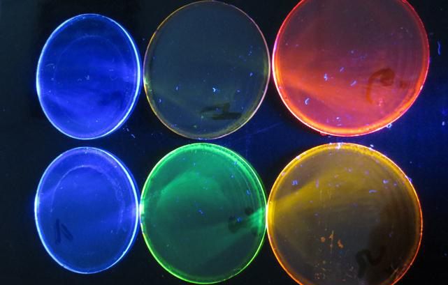
Innovation
Creativity
Customer-specific solutions
Content and Product Overview Photoresists
Photoresists
We deliver our products within 1 week ex work, in-stock stock items are delivered immediately or on the requested date.
Package sizes for resists: ¼ , 0.5 l (2 x ¼), 1 , 2.5 , 6 x 1 , 4 x 2.5 ; and for process chemicals: 1 l, 2.5 , 5 , 4 x 2,5 , 4 x 5 .
Information on Allresist products Page
General product information (overview, shelf life, waste water treatment, safety instructions) 5
Detailed instructions for optimum processing of photoresists 7
Product portfolio of all Allresist products (photoresists, e-beam resists, experimental samples) 64
Positive system Applications/properties Product Page
AR-P 1200 spray coating for various applications AR-P 1210, 1220, 1230 10
AR-P 3100 mask production, fine gradations, high resolution AR-P 3110, 3120, 3170 14
AR-P 3200 thick resist of high dimens. accuracy up to 40/100/20 µm AR-P 3210, 3220, 3250 18
AR-P 3500 (T) wide process range, high resolution AR-P 3510 (T), 3540 (T) 22
AR-P 3700 / 3800 high contrast, highest resolution, sub-µm AR-P 3740, 3840 26
AR-P 5300 undercut structures (one layer lift-off) AR-P 5320, 5350 30
Special system Applications/properties Product Page
AR-U 4000 image reversal – optionally positive or negative AR-U 4030, 4040, 4060 32
AR-PC 500(0) protective coating, 40 % KOH etch-stable AR-PC 503, 504, 5040 36
AR-BR 5400 bottom resist for 2L lift-off system (pos./neg.) AR-BR 5460, 5480 38
AR-P 5900 complicated patternings with hydrofluoric acid (5 %) AR-P 5910 44
Negative system Applications/properties Product Page
AR-N 2200 spray coating for various applications AR-N 2210, 2220, 2230 10
AR-N 4300 highest sensitivity, sub-µm, i-line, g-line AR-N 4340 46
AR-N 4400 films up to 100/ 50 µm, i-line, X-ray, e-beam AR-N 4400-50, 4400-25 50
Series CAR 44 films up to 20/ 10 µm, easy removable, AR-N 4400-10, 4400-05
additionally for lift-off structures AR-N 4450-10
AR-N 4600 (S/R) Thick negative resists for applications < 20 µm AR-N 4600-10, 4650-10 56
Process chemistry Applications/properties Product Page
Thinner safer solvent for photoresists AR 300-12 62
safer solvent (partly) for e-beam resists AR 600-01, -02, -07, -09
Developer buffer system for photo/ e-beam resists AR 300-26, 300-35 63
Developer metal ion-free for photo/ e-beam resists AR 300-44, -46, -47, -475 64
Remover organic solvents and aqeous-alkaline AR 600-70, 600-71, 300-70 65
As of: May 2019
solutions for photo/ e-beamresist AR 300-72, -73, 300-76
Adhesion promoter organic solutions for resists AR 300-80 new, HMDS 68
4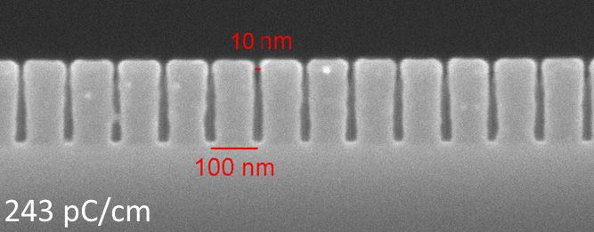
Innovation
                                                                      Creativity
                                                     Customer-specific solutions

     General Product Information on Allresist Photoresists

                                                                                                                               Photoresists
This general part explains and completes our individual photoresist product information and provides a first overview
as well as profound background knowledge. At www.allresist.de, you will find further information in our FAQ as well
as our resist-WIKI and a detailed collection of product parameters.
Overview of composition, mode of action and
specific properties of photoresists
Photoresists (photo coatings) are in particular used in mi-
croelectronics and microsystems technology for the fabri-
cation of µm- and sub-µm-structures.
Resists are in most cases applied by spin coating. For thin
resists, the optimum rotational speed ranges from 2000
to 4000 rpm, for thick resists between 250 and 2000 rpm.
Generally utilizable is a spin speed of up to 9000 rpm to
generate films of 30 nm to 200 µm depending on the re-
spective type of resist used. Thicker films of up to 1 mm
can be fabricated with casting procedures.
Alternative coating techniques are e.g. dip coating (for lar-   Negative photoresists like AR-N 4300, 4400 are compo-
ge and/or substrates with irregular surface geometry) and       sed of novolacs, acid generators and amine components
spray coating (for highly structured topologies, for compli-    (CAR) dissolved in solvents like e.g. methoxypropyl aceta-
cated substrate shapes) or roller coating procedures.           te (PGMEA).
                                                                After exposure and subsequent tempering step, the com-
Allresist offers a large variety of different types of re-
                                                                position of CAR leads to a crosslinking of the exposed
sists which cover a wide range of possible applications:
                                                                negative-tone resist film. Irradiated areas are consequently
Positive photoresists like e.g. AR-P 3100, 3200, 3500,          rendered insoluble and remain after development, while
3700 are composed of a combination of film forming              unexposed areas are still soluble and are dissolved by the
agents like e.g. cresol novolac resins and light-sensitive      developer.
components such as e.g. naphthoquinone diazide, which
                                                                Thick negative films up to 200 µm can be produced with
are for example dissolved in solvents like methoxypro-          CAR 44 (AR-N 4400). This resist which is highly sensitive
pyl acetate (equivalent to PGMEA). The addition of the          in a range between 300 - 440 nm and to synchrotron
light-sensitive component to the alkali-soluble novolac         radiation provides excellent structural quality.
results in a reduced alkaline solubility. After exposure
to UV light (308 - 450 nm) using an exposure mask, the
light-sensitive component is converted in exposed areas
into the corresponding indene carboxylic acid derivati-
ve which then increases the alkaline solubility of positive
resists by a factor of about 100. The refractive index of
novolac-based resists is in a range of 1.60. After deve-
lopment, only areas protected by the mask remain while
the exposed areas are dissolved. Photoresists provide an
excellent protection against etch media with pH-values
between 0 and 13.
Image reversal resists are the resists of the AR-U
4000 series which are positive resists containing an ad-        Resists for lift-off applications are the positive resist
ditional amine. Depending on the respective manu-               AR-P 5300 and the two-component resist system AR-
                                                                                                                                As of January 2014

facturing process, positive or negative images can be           BR 5400/AR-P 3510. Lift-off is also possible with negative
generated. Negative images are produced if an addi-             resists AR-N 4300 and 4450 as well as with the image
tional tempering step and a flood exposure of the en-           reversal resists AR-U 4000.
tire surface is performed after image-wise exposure.            Protective coatings like AR-PC 500 and 5000 are offered

                                                                                                                                      5
Innovation
                                    Creativity
                                    Customer-specific solutions

                           General Product Information on Allresist Photoresists
Photoresists

                     by Allresist for a large variety of applications, e.g. for the   these temperatures are maintained, resists in unopened
                     backside protection of processed wafers during KOH and           bottles are stable until expiry date (which is in general
                     HF etchings, for a mechanical protection during transport,       2 years after production), at least however for 6 month
                     or as insulating layer. Protective coatings are not light-       after date of sale. Brief temperatures deviations have no
                     sensitive and cannot be patterned if used alone. They can        influence on general product properties.
                     however be patterned with photoresists within the con-           If resists are to be used later than 6 month after date of
                     text of a two-layer system.                                      sale or to be processed within a very small process win-
                     Allresist also produces a wide range of special resists,         dow, storage at 4 – 8 °C is recommended. Exceptions
                     e.g. electroplating-stable resists like SX AR-P 5900/4 for       are only resists with recommended storage temperatu-
                     applications performed at a pH-value of 13.                      res between 18 – 25 °C. These resists should not be
                     For hydrofluoric acid etchings and BOE-processes (up             stored colder.
                     to 5 % HF), the 5 µm-resist AR-P 5910 (formerly X AR-P           Photoresists stored for several years are outdated and
                     3100/10) offers considerably better adhesion properties          may only be used with considerable restrictions. This also
                     than all other photoresists.                                     applies to resists stored at too high temperatures and to
                     For a patterning of glass/SiO2 substrates in concentra-          highly diluted resists which age faster than normal. Pos-
                     ted HF, the positive-tone two-component system SX AR-            sible consequences are the formation of particles which
                     PC 5000/40 – AR-P 3540 T or the negative-tone two-               is caused by a precipitation of the light-sensitive compo-
                     component system SX AR-PC 5000/40 –AR-N 4400-10                  nent. Repeated fine filtrations is however only helpful at
                     is recommended. The upper photoresist layer is initially         an early stage. The steadily declining concentration of the
                     developed under aqueous-alkaline conditions before the           light-sensitive component will successively lead to lower
                     lower SX AR-PC 5000/40 film is developed with solvents.          development rates, increased dark erosion and reduced
                                                                                      resist adhesion properties.
                     AR products are available both for the deep UV range
                     of 240 – 300 nm (AR-N 4300) as well as for the long-
                                                                                      Wastewater treatment
                     wavelength range up to 500 nm (SX AR-P 3500/6).
                                                                                      Up to 90 % of the organic material can be removed from
                     Temperature-stable resists up to 400 °C are the poly-
                                                                                      developer wastes if the pH of used aqueous alkaline de-
                     imide resists SX AR-PC 5000/80 and SX AR-P 5000/82.
                                                                                      veloper and remover solutions is adjusted to pH 9 to 10
                     User-oriented photoresists                                       by addition of acids, followed by subsequent separation of
                     Allresist is able to consider specific customer’s requests       the precipitate.
                     already in early stages of design and development of new         Prior to waste disposal, filtered solutions have to be ad-
                     photoresists, due to its high competence and flexibility. It     justed to pH 6.5 – 8.0. Solid wastes may be disposed of at
                     is thus possible to create a modified product according to       sanitary landfills or by incineration in officially authorized
                     the respective demands of each technology and to adapt           plants. Collected resist and solvent wastes have to be dis-
                     this product together on-site, if required.                      posed of in approved incinerators.
                     Just ask us! Based on our innovative experience potential
                     are we able to realise cost-efficient resist formulations also   Safety instructions
                     in small amounts within short time. More detailed investi-       Resists, thinner and remover contain organic solvents. Ade-
                     gations may then be conducted within the scope of R&D            quate ventilation in the working area is thus mandatory.
                     projects.                                                        Developer solutions are caustic alkaline liquids which may
                                                                                      irritate the skin. Avoid direct contact with products and
                     Stability and optimum storage conditions                         their vapours (wear safety goggles and gloves).
                     Photoresists are light-sensitive, they react to light expo-      EG-safety data sheets of our products may be downloa-
                     sure or high temperatures and also during storage, age-          ded from www.allresist.de/products or be requested at
                     related changes occur. Resists are therefore filled in light-
As of January 2014

                                                                                      info@allresist.de.
                     protected amber bottles, stored in a cool place and can
                     only be processed under yellow light (λ > 500 nm). The
                     date of expiry and the recommended storage tempera-
                     ture are indicated on the product label of each bottle. If

     6
Innovation
                                                                        Creativity
                                                       Customer-specific solutions

    Detailed Instructions for Optimum Processing of Photoresists

                                                                                                                                    Photoresists
0. Adhesion – substrate pre-treatment                              room temperature for a few hours prior to opening.
The adhesion between substrate and resist is of major im-          Air bubbles can be avoided if resist bottles are slightly ope-
portance for the safe processing of resists. Smallest changes      ned a few hours before coating to allow for pressure com-
of the cleaning procedure or the technology can exhibit a          pensation and then left undisturbed. Thick resists require
significant influence on the adhesive strength. Silicon, silicon   several hours for this process, thin resists need less time.
nitride and base metals (aluminium, copper) are generally          Applying the resist with caution and not too fast with a
characterised by good resist adhesion properties, while ad-        pipette or dispenser will also prevent bubbles and inho-
hesion is reduced on SiO2, glass, noble metals such as gold        mogeneities in the resist films.
and silver or on gallium arsenide. For these substrates, ad-       A repeated opening of resist bottles causes evaporation
hesion promoters are absolutely required to improve the            of the solvent and an increased viscosity of the resist. For
adhesion strength. High air humidity (> 60 %) also reduces         resist films with a thickness of 1.4 µm, a loss of only 1 % of
adhesion substantially.                                            the solvent already increases the film thickness by 4 %, thus
If new clean substrates (wafers) are used, a bake at appro-        requiring considerably higher exposure doses.
ximately 200 °C minutes (3 min, hot plate) is sufficient for       Generally used coating conditions are temperatures of 20
drying, but substrates should be processed quickly there-          to 25 °C with a temperature constancy of + 1 °C (opti-
after. A temporary storage in a desiccator is highly recom-        mum 21 °C) and a relative humidity of 30 to 50 % (opti-
mended in order to prevent rehydration.                            mum 43 %). Above a humidity of 70 %, coating is basically
Pre-used wafers or wafers which are contaminated with              impossible. The air moisture also affects the film thickness
organic agents require a previous cleaning in acetone, follo-      which is reduced with increasing humidity. For AR-P 3510,
wed by isopropanol or ethanol treatment and subsequent             the film thickness decreases by about 2 nm per each per-
drying if necessary. This procedure will improve adhesi-           cent of humidity.
on of the resist. If only acetone is used for cleaning, the
                                                                   At spin speeds of > 1500 rpm, 30 s are sufficient to obtain
substrate must be dried in a drying oven to remove the
                                                                   the desired film thickness. At lower spin speeds, the time
condensed moisture.
                                                                   should be extended to 60 s. For an exposure of rectangu-
If a technology involves repeated processing of wafers or          lar masks, usually a Gyrset (closed chuck) system is used,
subjecting these to various conditions, a thorough cleaning        which provides a beter film quality and reduces edge bead
is recommended. The cleaning procedure is however high-            formation. It has however to be taken into account that the
ly process- and substrate-dependent (and depends also on           film thickness decreases to approximately 70 % of the film
the structures already deposited). The use of removers or          thickness which is obtained with open chucks.
acids (e.g. piranha) for removal, followed by rinsing and
tempering, may be required. In very difficult cases, an ultra-     2. Tempering / Softbake
or megasonic cleaning may be helpful.                              Resists films which have been previously coated still contain,
To improve the adhesion features, adhesion-enhancing               depending on the film thickness, a substantial amount of
agents such as e.g. adhesion promoter AR 300-80 may be             residual solvent. A subsequent tempering at 90 – 100 °C is
used which is applied immediately before resist coating in a       performed to dry and to harden the resist films. In addition
very simple procedure by spin coating as thin layer of ap-         to improved resist adhesion properties, also the dark erosi-
prox. 15 nm thickness and tempered. It is also possible to         on during development is reduced by these means.
evaporate HMDS onto the substrates. The monomolecu-                The decision if a hot plate or a convection oven should
lar layer on the wafer surface has an adhesion-promoting           be preferred depends for thin films (< 5 µm) on the avai-
effect due to its hydrophobic properties which facilitate          lability, since technically none of the procedures offers a
adsorption of the resist.                                          particular advantage. The fast through-put of a hot plate is
                                                                   compensated by the option for batch tempering (approx.
1. Coating                                                         25 wafers in one step) in convection ovens. Drying thicker
Substrates should be cooled down prior to coating, and             films in a convection oven is however unfavourable since
                                                                                                                                     As of January 2014

resists have to be adjusted to the temperature of the (pre-        the dried resist surface inhibits a fast solvent evaporation.
ferably air-conditioned) working area. If the resist is too        In these cases, a hot plate is recommended because more
cold, air moisture precipitates on the resist. Bottles remo-       solvent is expelled from the bottom of the resist film.
ved from the refrigerator should therefore be warmed to

                                                                                                                                           7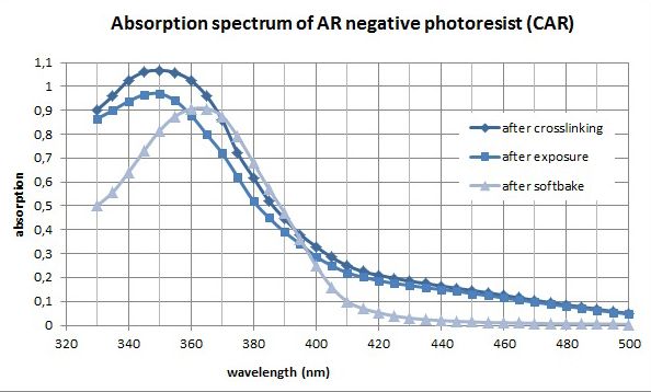
Innovation
                                    Creativity
                                    Customer-specific solutions

                        Detailed Instructions for Optimum Processing of Photoresists
Photoresists

                     Insufficiently tempered resist films (either too short or at      on the desired resolution. The maximum resolution requi-
                     too low temperatures) entail a variety of further problems.       res the highest exposure dose.
                     Air bubbles may develop successively which are due to an          The dose to clear unexposed areas of negative resists is in
                     evaporation of residual solvent. Possible consequences are        a range of 30 - 40 s for films with a thickness of 1 - 2 µm.
                     inaccurate structural images, a roundening of resist profiles     This exposure dose which produces a layer buildup of >
                     as well as unacceptable high dark erosion during develop-         90 % should accordingly be increased by 10 - 20 % for pat-
                     ment.                                                             terning undil. poses. For thick films of more than 100 µm,
                     If temperature-sensitive substrates are processed it is also      development times of more than 1 hour may be required.
                     possible to work at considerably lower softbake tempera-          Coated and tempered resist films can be stored for several
                     tures (< 60 °C). The development regime has to be adjus-          weeks prior to exposure without quality loss. Photoresists
                     ted accordingly.                                                  are however more sensitive directly after coating as com-
                     If the hard bake of resist films was too rigid (temperature       pared to layers which were stored for several hours or
                     too high or tempered too long), a partial destruction of          days. The decrease in sensitivity is approximately 3 % after
                     the light-sensitive component results which significantly in-     3 h, 6 % after 72 h, and 8 % after 72 hours (in relation to
                     creases exposure times and reduces the sensitivity.               the initial value) and remains then more or less constant
                     After the softbake, substrates are cooled to room tempera-        for several weeks.
                     ture prior to further use. Especially thick resists require an
                                                                                       4. Development
                     appropriate waiting time for rehydration before exposure.
                                                                                       During development, positive resist films are structured
                     3. Exposure                                                       by dissolving exposed areas, while unexposed areas are
                     The exposure is performed through masks in suitable ex-           removed if negative resists are developed. For reprodu-
                     posure systems such as e.g. steppers (i-, g-line), mask alig-     cible results, temperatures between 21 and 23 °C with a
                     ners or contact exposure systems in the respective spect-         temperature constancy of ± 0.5 °C should be maintained.
                     ral working range. Direct laser exposure without masks is         All offered developers (AR 300-35, AR 300-26, AR 300-40)
                     also possible.                                                    are suitable both for immersion and puddle development,
                     AR photo coatings are light-sensitive in the broad band UV        while developers AR 300-26 and 300-40 can additionally
                     range (300 - 450 nm) and thus also at the typical emission        be used for spray development.
                     lines of mercury at 365 nm (i-line), 405 nm (h-line), and         Optimally adapted developers and dilutions for each resist
                     436 nm (g-line) (→ Absorption spectra), with maximum              are specified in the product information. Entries like for
                     sensitivity in the g- and h-line range. Values for recommen-      example AR 300-26 1 : 2 indicate a dilution of 1 part of
                     ded exposure dose as specified in our product informati-          developer AR 300-26 with 2 parts of DI water.
                     on are only guideline values determined for our standard          The optimal development time is dependent on the respec-
                     processes and have to be confirmed accordingly in own             tive resist type and film thickness as well as on the exposure
                     experiments.                                                      wavelength, tempering and development procedure. Favou-
                     Air bubbles may develop either during or after exposure           rable development times for films of up to 2 µm are e.g. for
                     and are e.g. caused by too high light doses or exposure           immersion or puddle development in a range between 20
                     intensities. This can be avoided if the optimum light dose        and 60 s and should not exceed 120 s.
                     is determined by exposure bracketing or in several con-           Layers of up to 10 µm thickness require 2 to 10 min, while
                     secutive exposure steps with intermediate pauses. A too           films with thickness values of up to 100 µm may need de-
                     short or too low tempering after coating results in insuf-        velopment times of more than 60 min. The more intensive
                     ficient drying of the resist film, since still too much solvent   spray developments require shorter times.
                     is present in the films which causes bubble formation due         Developer concentrations as listed in our product informa-
                     to outgassing.                                                    tion were determined for specific film thickness values or
As of January 2014

                     The exposure dose which is required to develop a lar-             process parameters and can only serve as guideline values
                     ge area of positive resists without structures in a suitable      under other conditions. The exact developer concentra-
                     development time is called “dose to clear”. This exposure         tion has always to be adjusted to specific demands (film
                     dose should be increased slightly for patterning, depending       thickness, development time, tempering).

     8
Innovation
                                                                        Creativity
                                                       Customer-specific solutions

    Detailed Instructions for Optimum Processing of Photoresists

                                                                                                                                Photoresists
The parameters contrast and sensitivity are adjusted via the      7. Customer-specific technologies
developer concentration by defined dilution of the devel-         Generation of semiconductor properties
oper with DI water.                                               The produced resist mask is utilised for technological pro-
Note: Metal ion-free developers are more sensitive to di-         cesses according to the user’s requirements. Semiconduc-
lution differences than buffered systems. These developers        tor properties are generated in a user-specific manner,
should be diluted immediately prior to use and extremely          e.g. by boron or phosphorous doping, by etch proces-
thoroughly, if possible with scales, in order to assure repro-    ses or by formation of conductor paths. Thereafter, the
ducible results.                                                  resist is in most cases no longer needed and removed.
Higher developer concentrations formally result in an in-
creased light sensitivity of positive resist developer systems.   8. Removal
The required exposure energy is minimised and the deve-           For the removal of softbaked resist films, polar solvents
lopment time is reduced, which allows for a high process          like e.g. the thinner AR 300-12 and remover AR 600-70
throughput. Possible disadvantages are an increased dark          are suitable.
erosion and (in some cases) a too low process stability
                                                                  For the wet chemical stripping of tempered resist films,
(too fast). Negative resists require a higher exposure dose
                                                                  the organic, highly versatile removers AR 300-70, AR 300-
for crosslinking at higher developer concentrations.
                                                                  72 and AR 300-76 are available which may be heated to
Lower developer concentrations provide a higher contrast          80 °C to reduce the dissolution time. Due to a classifica-
for positive resist films and reduce resist erosion in unex-      tion of the raw material NEP (Ar 300-70 and -72) as toxic
posed regions or only partly exposed interface areas even         for reproduction, Allresist strongly recommends to use
at longer development times. This particularly selective          the newly introduced, less harmful remover AR 300-76
working method ensures a high detail rendition.                   which is equivalent with respect to its dissolving power.
The effectiveness of the developing bath for immersion            Remover AR 300-73 which was designed for special re-
development is limited by factors such as process through-        sists may be heated to 50 °C, does however attack alumi-
put and CO2 absorption from air. The throughput depends           nium surfaces.
on the fraction of exposed areas. CO2 absorption is also
                                                                  Remover AR 600-71 which is already highly efficient at
caused by frequent opening of the developer bottle and
                                                                  room temperature is particularly suitable for customers
leads to a reduced development rate. This effect is avoi-
                                                                  who are able to use removers with low flash point.
ded by if the surface of the developer bath is kept under
nitrogen.                                                         In semiconductor industries, the removal (stripping) is
                                                                  mostly performed by ashing in a plasma asher. The O2-
5. Rinse                                                          plasma generated by microwave excitation is used for an
After development, substrates have to be rinsed imme-             isotropic etching of the photoresist. But also oxidising
diately with deionised water until all residual developer is      acid mixtures (piranha, nitrohydrochloric acid, nitric acid
completely removed, and subsequently dried.                       and others) may be applied in wet chemical removal pro-
                                                                  cedures.
6. Postbake / hardbake
For specific process steps, a postbake at approximately 110
°C leads to a higher etch stability during wet-chemical and
plasma-chemical etching procedures. Higher temperatures
are possible for stronger etch conditions, may however
result in a rounding of resist profiles.
Structures in very thick films (> 5 µm) may even converge.
                                                                                                                                 As of December 2014

UV curing (short wave deep UV exposure with simulta-
neous heating of the wafer to up to 180 °C, if required)
leads to strong hardening of resist structures. While the
melting of structures is now prevented in most cases, a
subsequent removal is extremely difficult.

                                                                                                                                       9
Innovation
                                   Creativity
                                   Customer-specific solutions

                    Positive / Negative Photoresists AR-P 1200 / AR-N 2200
Photoresists

                    AR-P 1200 / AR-N 2200 resist series for spray coating
                    Ready-to-use positive and negative spray resists for various applications

                    Characterisation                                        Properties I
                    - broadband UV, i-line, g-line                           Parameter / AR-P                1210         1220         1230
                    - AR-P 1210 /AR-N 2210 positive/negative resists                      AR-N               2210         2220         2230
                      for a uniform coverage of vertical trenches
                                                                             Solids content (%)                4           4             4
                    - AR-P 1220 /AR-N 2220 for etch profiles
                                                                             Film thickness (µm)             4 - 10       3-8         0.5 - 1
                      with 54° slopes
                    - AR-P 1230 /AR-N 2230 for planar wafers                 Resolution (µm)                  1.0          1.0          1.0
                    - good adhesion, smooth surface                          Contrast                         3.0          3.0          3.0
                    - combination of novolac and naphthoquinone diazide      Flash point (°C)                   1           9           37
                    - safer solvent PGMEA as well as methyl ethyl ketone     Storage 6 month (°C)                        10 - 18

                    Structure resolution                                    Properties II
                                                                             Glass transition temperature                 108
                                                                             Dielectric constant                           3.1
                                                                             Cauchy coefficients                  N0             1.625 / 1.595
                                                 AR-N 2210
                                                                             AR-P 1220 / AR-N 2220                N1              74.4 / 72.5
                                                 Film thickness 5 µm
                                                 Resolution up to 1.4 µm                                          N2              170 / 85.0
                    Process parameters                                       Plasma etching rates (nm/min)   Ar-sputtering          8/8
                                                                             (5 Pa. 240-250 V bias)               O2              169 / 173
                     Substrate       Si 6‘‘ wafer
                                                                                                                  CF4              38 / 33
                     Tempering       82 °C, chuck
                                                                                                                80 CF4             90 / 93
                     Exposure        broadband (h-, g-, i-line)
                                                                                                               + 16 O2
                     Development     AR 300-44, 4 min puddle

                    Parameters spray coater “EVG® 150”
                     Spray coater                            Positive resist                 Negative resist
                     EVG® 150, EV Group                      AR-P 1210                       AR-N 2210
                     Resist flow (drops/min)                 25                              25
                     Arm speed (mm/s)                        200                             200
                     N2 pressure (kPa)                       50                              50
                     Exposure                                EVG® 6200NT Automated Mask Alignment System
                     Sensitivity (film thickness)            170 mJ/cm2 , 4,5 µm             50 mJ/cm2 , 4,5 µm
                     Development with AR 300-44              1:30 min                        2 min
                     Minimum resolution (µm)                 1.4                             1.4
As of August 2016

                    Process chemicals
                     Developer               AR 300-44
                     Remover                 AR 300-76, AR 300-73

 10
Innovation
Creativity
Customer-specific solutions
Positive / Negative Photoresists AR-P 1200 / AR-N 2200
Photoresists
P ro c e ss conditions
This diagram shows exemplary process steps for AR-P/N 1200/2200 resists with the EVG® 150. All specifications
are guideline values which have to be adapted to own specific conditions. For further information on processing,
“Detailed instructions for optimum processing of photoresists”. For recommendations on waste water treatment
and general safety instructions, ”General product information on Allresist photoresists”.
Coating AR-P 1210 AR-P 1220 AR-P 1230
AR-N 2210 AR-N 2220 AR-N 2230
5 µm 3 µm 1.0 µm
Tempering (±1 °C) For heated chucks: 70 - 80 °C without further drying
For non-heated chucks:
90 °C, 2 min hot plate or 85 °C, 25 min convection oven
UV exposure Broadband UV, 365 nm, 405 nm, 436 nm
Exposure dose (E0, EVG® 6200NT Automated Mask Aligner):
AR-P 1210: 170 mJ/cm2, 4,5 µm; AR-N 2210: 50 mJ/cm2, 4,5 µm
Cross-linking bake for 90 °C, 5 min hot plate or
AR-N 2210-2230 85 °C, 25 min convection oven
Development AR 300-44 AR 300-44 AR 300-44
(21-23 °C ± 0.5 °C) puddle 4 min 3 : 1, 5 min 2 : 1, 6 min
Rinse DI-H2O, 30 s
Post-bake Not required
(optional)
Customer-specific Generation of semi-conductor properties
technologies
Removal AR 300-70 or O2 plasma ashing
As ofMarch 2017
Copyright EVG
5 µm resist structures of AR-N 2220 in 150 µm deep etch grooves Aluminium conductor paths after etching
Important processing instructions regarding single process steps are described on the following page
11Innovation
Creativity
Customer-specific solutions
Positive / Negative Photoresists AR-P 1200 / AR-N 2200
Photoresists
Processing Instructions for Spray Resists
Coating: For spray coating, resists are filled into the cart- prox. 200 mJ/cm². Negative-tone resists with approx. 70
ridges of the spray coater under yellow light. Gas forma- mJ/cm² are substantially more sensitive and require shorter
tion in the resist supply line which is generally observed exposure times, which is advantageous for the exposure
for AZ 4999 does not occur with AR resists. of wafers with extreme topologies in order to prevent un-
The quality of the coating largely depends upon the desirable reflexions.
respective spray coating device which is used. The best Thin films generated with AR-P 1230 and AR-N 2230 re-
experiences we have had with the devices of EV Group. quire lower exposure doses.
Adjustable device parameters such as dispensing rate, For negative resists, a cross-linking bake after exposure is
scanning speed, spray distance and chuck temperature mandatory!
exhibit a major influence on the film forming process.
Commercially available spraying devices differ conside- Development: The development time strongly depends on
rably with respect to their coating properties, and own the respective film thickness and amounts to approximately
experiments to determine the optimum parameters 5 minutes for 5 μm films. If edges are only marginally co-
are therefore absolutely necessary. vered, a 3 : 1 dilution (3 parts developer : 1 part water) is
Resists 1220/2220 and 1230/2230 form very homoge- recommended. For the development of thin films of about
neous surfaces. Due to their specific solvent composi- 0.5 μm, the developer should be diluted up to 2 : 1.
tion, solvent evaporation is reduced, but nevertheless
a complete and at the same time sufficient coverage of
the substrate is provided. Surfaces are thus considerab-
ly less rough as compared to AZ 4999.
If unheated chucks are used, coated substrates should
be tempered on a hot plate at plate at 85 - 90 °C for
2-5 min or in a convection oven at 85 °C for 25 min
to improve adhesion. A temperature of 90 °C should
however not be exceeded to prevent edge retraction
of the resist caused by possible softening processes. Copyright EVG
With resists AR-P 1210 and 1220 as well as with Lift-off structures with AR-N 2220 after spray coating
AR-N 2210 and 2220 and under standard conditions,
film thickness values of 4 - 8 μm can be obtained. Hig-
her film thicknesses are possible with higher dispensing
rates or using multiple coating steps.
In comparison with AZ 4999, these resists have a lo-
wer tendency to form disturbing beads. Resists AR-P
1230 and AR-N 2230 are thus well suited for the ge-
neration of thin films with a thickness of 0.5 - 1 μm and
can be used for spray coating as well as for spin coating
applications. The thickness of films produced via spin Copyright EVG
coating ranges between 50 to 120 nm. Very good coverage of groove bottom and of upper edge
Exposure: For an exposure of positive resists, the enti-
re UV-range of 300 to 450 nm can be utilised, while for
As of March 2017
the exposure of negative resists, a range between 300
to 436 nm is recommended. The exposure time gene-
rally depends on the film thickness. For a film thickness
of about 5 μm, the sensitivity of positive resists is ap-
12Innovation
Creativity
Customer-specific solutions
13Innovation
Creativity
Customer-specific solutions
Positive Photoresist AR-P 3100
Photoresists
AR-P 3100 photoresist product series for mask production
Adhesion-enhanced positive resists for the production of masks and fine scale divisions
Characterisation Properties I
- broadband UV, i-line, g-line Parameter / AR-P 3110 3120 3170
- high photosensitivity, high resolution
Solids content (%) 28 21 8
- strong adhesion to critical glass/chromium surfaces for
Viscosity 25 °C (mPas) 12 5 2
extreme stresses during wet-chemical etching processes
Film thickness/ 4000 rpm (nm) 1000 550 120
- for the production of CD masters and lattice structures
- 3170 also suitable for laser interference lithography Resolution (µm) 0.5 0.4 0.4
- plasma etching resistant Contrast 3.0 3.0 3.0
- combination of novolac and naphthoquinone diazide Flash point (°C) 42
- safer solvent PGMEA Storage 6 month (°C) 10 - 18
Spin curve Properties II
Glass transition temperature 108
Dielectric constant 3.1
Cauchy coefficients N0 1.621
N1 65.6
N2 195.6
Plasma etching rates (nm/min) Ar-sputtering 7
(5 Pa, 240-250 V bias) O2 165
CF4 38
80 CF4 89
+ 16 O2
Structure resolution Resist structures
AR-P 3120 70-nm-lines generated with the
Film thickness 0.6 µm AR-P 3170 by laser interference
Resist structures 0.38 µm L/S lithography
Process parameters Process chemicals
As of Octobber 2019
Substrate Si 4‘‘ wafer Adhesion promoter AR 300-80
Tempering 95 °C, 90 s, hot plate Developer AR 300-26, AR 300-47
Exposure i-line stepper (NA: 0.65) Thinner AR 300-12
Development AR 300-47, 1 : 1, 60 s, 22 °C Remover AR 300-76, AR 300-73
14Innovation
Creativity
Customer-specific solutions
Positive Photoresist AR-P 3100
Photoresists
P ro c ess conditions
This diagram shows exemplary process steps for AR-P 3100 resists. All specifications are guideline values which
have to be adapted to own specific conditions. For further information on processing, “Detailed instructions for
optimum processing of photoresists”. For recommendations on waste water treatment and general safety instruc-
tions, ”General product information on Allresist photoresists”.
Coating AR-P 3110 AR-P 3120 AR-P 3170
4000 rpm, 60 s 4000 rpm, 60 s 4000 rpm, 60 s
1000 nm 550 nm 120 nm
Tempering (+/- 1 °C) 100 °C, 1 min hot plate or
95 °C, 25 min convection oven
UV exposure Broadband UV, 365 nm, 405 nm, 436 nm
Exposure dose (E0, broadband UV stepper):
70 mJ/cm² 65 mJ/cm² 60 mJ/cm²
Development AR 300-26 2 : 5 AR 300-47, 5 : 1 AR 300-47, 3 : 1
(21-23 °C ± 0,5 °C) puddle 60 s 60 s 60 s
Rinse DI-H2O, 30 s
Post-bake 115 °C, 1 min hot plate or
(optional) 115 °C, 25 min convection oven
Customer-specific Generation of e.g. semi-conductor properties
technologies
Removal AR 300-70 or O2 plasma ashing
Development recommendations
Resist / Developer AR 300-26 AR 300-35 AR 300-47
AR-P 3110 1 : 2 to 1 : 3 pure 6:1
AR-P 3120 1:3 5:1 5:1
AR-P 3170 1:4 2:1 3:1
As of October 2019
15Innovation
Creativity
Customer-specific solutions
Positive Photoresist AR-P 3100
Photoresists
Linearity Optimum exposure dose
Up to a structure width of 0.38, a very good agreement is obtained. Underexposure leads in the case of complete development (more
REM measurement: Thickness 560 nm, i-line stepper (NA: 0.65 than 55 ml/cm2) to narrower trenches, while overexposure results
NA), Developer AR 300-47 1 : 1. in a widening of trenches.
Focus variation Focus variation (with and without PEB)
The intended structure sizes can here be realised by varying the Without PEB, a higher resolution is obtained since the focus curve
focus between -1.5 to 0.8 (parameter see grafic linearity). is steeper (PEB, 90 °C, 60 s).
Optimum exposure dose Thermal properties of resist structures
As of January 2016
Optimum dose, with hard bake (110 °C) and without hard bake. The Untempered Hard bake 115 °C
additional hard bake requires 15 % more light (PEB, 90 °C, 60 s).
16Innovation
Creativity
Customer-specific solutions
17Innovation
Creativity
Customer-specific solutions
Positive Photoresist AR-P 3200
Photoresists
AR-P 3200 photoresist series for high film thicknesses
Thick positive resists for electroplating and microsystems technology
Characterisation Properties I
- broadband UV, i-line, g-line Parameter / AR-P 3210 3220 3250(T)
- high photosensitivity, high resolution
Solids content (%) 47 47 39
- profiles with high edge steepness dimens. accuracy
Viscosity 25 °C (mPas) 1990 1820 250
- plasma etch resistant, electroplating-stable
- 3210/ 3250 for film thicknesses up to 40 µm/ 20 µm
Film thickness/ 4000 rpm (µm) 10 10 5
- 3220 transparent for thick films up to 100 µm in mul- Resolution (µm) 4.0 3.0 1.2
tiple coating steps, 100 µm development in one step Contrast 2.0 2.0 2.5
- combination of novolac and naphthoquinone diazide Flash point (°C) 42
- safer solvent PGMEA Storage 6 month (°C) 10 - 18
Spin curve Properties II
Glass transition temperature 108
Dielectric constant 3.1
Cauchy coefficients N0 1.597
AR-P 3210 N1 79.5
N2 105.1
Plasma etching rates (nm/min) Ar-sputtering 7
(5 Pa, 240-250 V bias) O2 170
CF4 39
80 CF4 90
+ 16 O2
Structure resolution Resist structures
AR-P 3210
Film thickness 12 µm AR-P 3220
Resist structures 4 µm Film thickness 25 µm
Process parameters Process chemicals
Substrate Si 4“ wafer
As of January 2018
Adhesion promoter AR 300-80
Tempering 95 °C, 10-15 min, hot plate Developer AR 300-26
Exposure Maskaligner MJB 3, contact exposure Thinner AR 300-12
Development AR 300-26, 1 : 3, 3 min, 22 °C Remover AR 300-76, AR 600-71
18Innovation
Creativity
Customer-specific solutions
Positive Photoresist AR-P 3200
Photoresists
P ro c ess conditions
This diagram shows exemplary process steps for AR-P 3200 resists. All specifications are guideline values which
have to be adapted to own specific conditions. For further information on processing, “Detailed instructions for
optimum processing of photoresists”. For recommendations on waste water treatment and general safety instruc-
tions, ”General product information on Allresist photoresists”.
Coating AR-P 3210 AR-P 3220 AR-P 3250 AR-P 3250T
4000 rpm, 90 s 600 rpm, 4000 rpm, 4000 rpm,
10 µm 120 s; 30 µm 60 s; 5.0 µm 60 s; 5.0 µm
Tempering (± 1 °C) H* 95 °C, 4 min 95 °C, 15 min 95 °C, 2 min 95 °C, 2 min
H* = hot plate or C* = convection oven C* 90 °C, 40 90 °C, 90 min 90 °C, 30 min 90 °C, 30 min
min
UV exposure Broadband UV, 365 nm, 405 nm, 436 nm
Exposure dose (E0, broadband UV stepper):
450 mJ/cm² 900 mJ/cm² 220 mJ/cm² 300 mJ/cm²
Development AR 300-26, 1 : 2 AR 300-26, AR 300-26, AR 300-44,
(21-23 °C ± 0,5 °C) puddle 2 min undil.; 3 min 3 : 2; 2 min pur; 2 min
Rinse DI-H2O, 30 s
Post-bake (optional) Not required
Customer-specific Generation of e.g. semi-conductor properties, galvanic, MEMS
technologies
Removal AR 300-76 or O2 plasma ashing
Processing instructions (for the processing of thick films > 40 µm)
Coating: Coating should be performed in two or several steps using the same procedure. After a low initial spin
speed (30 s), a main spin speed of 250 – 500 rpm for at least 2-5 min should be chosen. A brief subsequent spinning
off at 600 – 800 rpm for 5 s reduces edge bead formation.
Tempering: Tempering should be performed in 2 steps: 1. 75 °C, 5 min hot plate or 70 °C, 30 min convection oven;
2. 90 °C, 20 min hot plate or 90 °C, 80 min convection oven. After tempering, a slow cooling is recommended to
avoid stress cracks.
Development recommendations
As of March 2017
Resist / Developer AR 300-26 AR 300-35 AR 300-44
AR-P 3210 (up to 20 µm) 1 : 2 to 1 : 3 (2-10 min) undil. up to 10 µm (2-10 min) -
AR-P 3220 (up to 20 µm) 3 : 1 to 2 : 1 (2-5 min) - -
AR-P 3250 (up to 10 µm) 2 : 1 to 3 : 2 (1-5 min) - -
AR-P 3250T (up to 5 µm) - - undil. up to 5 µm (1-5 min)
19Innovation
Creativity
Customer-specific solutions
Positive Photoresist AR-P 3200
Photoresists
Sensitivity vs. duration of the soft bake Residual solvent after tempering
After 2 hours, the sensitivity remains more or less constant After a bake at 95 °C, approx. 7 % of the solvent remain in the layer
(broadband UV, resist thickness 20 µm). (initial solids content: 47 %)
Sensitivity in different developers Dark erosion in different developers
Film thickness 20 µm, soft bake 85 °C, 1 h convection oven, bb UV Erosion corresponding to determined sensitivities
Grey tone mask lithography Photolysis of photo-active compound (PAC)
As of December 2014
28 µm-high 3 D pyramids with AR-P 3220 Chemical reaction for bleaching and full exposure of the layer (Süss-
reaction)
The transparency of AR-P 3220 is higher as compared to AR-P 3210, due to the lower concentration of the PAC.
The gradation is accordingly relatively low. This fact can be used for the fabrication of three-dimensional structures
using grey tone masks with AR-3220. Different exposure doses will result in different resist film thicknesses.
20Innovation
Creativity
Customer-specific solutions
21Innovation
Creativity
Customer-specific solutions
Positive Photoresists AR-P 3500 / 3500 T
Photoresists
AR-P 3500 (T) photoresist series with wide process range
Sensitive positive-tone standard resists for the production of integrated circuits
Characterisation Properties I
- broadband UV, i-line, g-line Parameter / AR-P 3510 / 3510 T 3540 / 3540 T
- high photosensitivity, high resolution
Solids content (%) 35 / 32 31 / 28
- very good adhesion properties
Viscosity 25 °C (mPas) 33 / 38 18 / 21
- 3500 T: robust processing, suitable for TMAH
developer 0.26 n
Film thickness / 4000 rpm (µm) 2.0 1.4
- plasma etching resistant, temperature-stable up Resolution (µm) 0.8 / 0.6 0.7 / 0.5
to 120 °C Contrast 4.0 / 4.5 4.5 / 5.0
- combination of novolac and naphthoquinone diazide Flash point (°C) 42
- safer solvent PGMEA Storage 6 month (°C) 10 - 18
Spin curve Properties II
Glass transition temperature 108
Dielectric constant 3.1
Cauchy coefficients N0 1.627
AR-P 3540 T N1 71.4
N2 164.8
Plasma etching rates (nm/min) Ar-sputtering 7
(5 Pa, 240-250 V bias) O2 165
CF4 37
80 CF4 88
+ 16 O2
Structure resolution Temperature stability
AR-P 3540 T
Film thickness 1.5 µm
Resist structures 0.5 µm Structures without hard bake and with tempering at 140 °C (hot plate, 1
mm) with AR-P 3540
Process parameters Process chemicals
Substrate Si 4“ wafer Adhesion promoter AR 300-80
As of January 2014
Tempering 95 °C, 90 s, hot plate Developer AR 300-26, T: AR 300-44
Exposure g-line stepper (NA: 0.56) Thinner AR 300-12
Development AR 300-44, 60 s, 22 °C Remover AR 300-76, T: AR 300-76
22Innovation
Creativity
Customer-specific solutions
Positive Photoresists AR-P 3500 / 3500 T
Photoresists
P ro c ess conditions
This diagram shows exemplary process steps for AR-P 3500 (T) resists. All specifications are guideline values which
have to be adapted to own specific conditions. For further information on processing, “Detailed instructions for
optimum processing of photoresists”. For recommendations on waste water treatment and general safety instruc-
tions, ”General product information on Allresist photoresists”.
Coating AR-P 3510 AR-P 3540 T
4000 rpm, 60 s, 4000 rpm, 60 s,
2.0 µm 1.4 µm
Tempering (± 1 °C) 100 °C, 1 min, hot plate or
95 °C, 25 min, convection oven
UV exposure Broadband UV, 365 nm, 405 nm, 436 nm
Exposure dose (E0, broadband UV stepper):
55 mJ/cm² 120 mJ/cm²
Development AR 300-26, 1 : 5 AR 300-44
(21-23 °C ± 0,5 °C) puddle 60 s 60 s
Rinse DI-H2O, 30 s
Post-bake 115 °C, 1 min hot plate or
(optional) 115 °C, 25 min convection oven
Customer-specific Generation of semiconductor properties or lift-off
technologies
Removal AR 300-70 or O2 plasma ashing
Development recommendations
Resist / Developer AR 300-26 AR 300-35 AR 300-40
AR-P 3510, 3540 1:5 1:1 300-47, 1 : 1
AR-P 3510 T, 3540 T 1:2 undil. 300-44
Focus width AR-P 3540 T g-line stepper Resist structures
Ridge DOF @ 230 mJ Dose range
1.5 µm > 2.0 µm 110-260 mJ/cm²
As of January 2014
1.0 µm > 1.5 µm 130-260 mJ/cm²
0.7 µm > 1.25 µm 160-250 mJ/cm²
AR-P 3500
0.5 µm > 1.0 µm 190-240 mJ/cm² Film thickness 2 µm
Resist structures 5 µm
Best edge steepness: 180-200 mJ/cm²
23Innovation
Creativity
Customer-specific solutions
Positive Photoresists AR-P 3540 T
Photoresists
Focus width
Film thickness 1.5 µm on Si-wafer, dose: 230 mJ/cm2
Focus 1.5 µm L/S 1.0 µm L/S 0.7 µm L/S 0.5 µm L/S
- 1.0
- 0.75
- 0.5
- 0.25
0.0
+ 0.25
+ 0.5
+ 0.75
As of January 2014
Tempering: 95 °C, 90 s, hot plate (contact), exposure: g-line stepper (NA: 0.56; 0.75 s).
Development: AR 300-44, 60 s, 22 °C, puddle
24Innovation
Creativity
Customer-specific solutions
Positive Photoresists AR-P 3540 T
Photoresists
Linearity
Film thickness 1.5 µm on Si-wafer, focus: 0.0
Dose 1.5 µm L/S 1.0 µm L/S 0.7 µm L/S 0.5 µm L/S
160 mJ
190 mJ
210 mJ
230 mJ
Dark field erosion
Film thickness 1.5 µm on Si-wafer, focus: 0.0
Dose 1.5 µm L/S 1.0 µm L/S 0.7 µm L/S 0.5 µm L/S
190 mJ
210 mJ
230 mJ
As of January 2014
Tempering: 95 °C, 90 s, hot plate (contact), exposure: g-line stepper (NA: 0.56; 0.75 s).
Development: AR 300-44, 60 s, 22 °C, puddle
25Innovation
Creativity
Customer-specific solutions
Positive Photoresists AR-P 3700 / 3800
Photoresists
AR-P 3700 / 3800 photoresists for sub-µm structures
Sensitive positive-tone standard resists for the production of highly integrated circuits
Characterisation Properties I
- broadband UV, i-line, g-line Parameter / AR-P 3740 3840
- high sensitivity, highest resolution up to 0.4 µm
Solids content (%) 29 29
- high contrast, excellent dimensional accuracy
Viscosity 25 °C (mPas) 22 22
- optimised coating properties on topologically
complex substrate surfaces
Film thickness / 4000 rpm (µm) 1.4 1.4
- 3840 coloured to prevent the effect of standing waves Resolution (µm) 0.4 0.4
- plasma etching resistant, stable up to 120 °C Contrast 6.0 6.0
- combination of novolac and naphthoquinone diazide Flash point (°C) 42
- safer solvent PGMEA Storage 6 month (°C) 10 - 18
Spin curve Properties II
Glass transition temperature 108
Dielectric constant 3.1
Cauchy coefficients N0 1.623
AR-P 3740 N1 81.8
N2 160.4
Plasma etching rates (nm/min) Ar-sputtering 8
(5 Pa, 240-250 V bias) O2 164
CF4 38
80 CF4 88
+ 16 O2
Structure resolution Resist structures
AR-P 3740 AR-P 3740
Film thickness 1.1 µm Film thickness 1.8 µm
Resist structures 0.5 µm L/S Resist structures up to 1.0 µm
Process parameters Process chemicals
Substrate Si 4“ wafer Adhesion promoter AR 300-80
As of January 2014
Tempering 100 °C, 90 s, hot plate Developer AR 300-47, AR 300-26
Exposure i-line stepper (NA: 0.65) Thinner AR 300-12
Development AR 300-47, 60 s, 22 °C Remover AR 300-76, AR 600-71
26Innovation
Creativity
Customer-specific solutions
Positive Photoresists AR-P 3700 / 3800
Photoresists
P ro c ess conditions
This diagram shows exemplary process steps for AR-P 3700 / 3800 resists. All specifications are guideline values which
have to be adapted to own specific conditions. For further information on processing, “Detailed instructions for
optimum processing of photoresists”. For recommendations on waste water treatment and general safety instruc-
tions, ”General product information on Allresist photoresists”.
Coating AR-P 3740 AR-P 3840
4000 rpm, 60 s 4000 rpm, 60 s
1.4 µm 1.4 µm
Tempering (± 1 °C) 100 °C, 1 min hot plate or
95 °C, 25 min convection oven
UV exposure Broadband UV, 365 nm, 405 nm, 436 nm
Exposure dose (E0, broadband UV stepper):
55 mJ/cm² 72 mJ/cm²
Development AR 300-47 AR 300-47
(21-23 °C ± 0.5 °C) puddle 60 s 60 s
Rinse DI-H2O, 30 s
Post-bake 115 °C, 1 min hot plate or
(optional) 115 °C, 25 min convection oven
Customer-specific Generation of semiconductor properties
technologies
Removal AR 300-70 or O2 plasma ashing
Development recommendations
Resist / Developer AR 300-26 AR 300-35 AR 300-40
AR-P 3740, 3840 1:3 4:1 300-46 high speed
300-47 high contrast
As of January 2014
27Innovation
Creativity
Customer-specific solutions
Positive Photoresists AR-P 3700 / 3800
Photoresists
Dark erosion
AR-P 3740 may be developed with any of the four TMAH develo- Using a dilution series of AR 300-26, the desired development pro-
pers. A high sensitivity is associated with high erosion rates. No dark perties can be adjusted accordingly. A dilution of 3:2 (3 parts AR
erosion is obtained if weaker developers are chosen (see diagram 300-26, 2 parts DI water) is not recommended, due to the high
Influence of developer strength) erosion rate. More suitable in this case is a dilution of 1 : 1 to 2 : 1.
Influence of developer strength of the dark erosion Influence of developer strength of exposure dose
Using coated Cr-substrates (thickness 1.5 µm), 15 – 350 nm are removed Using the strong developer AR 300-46, short exposure times can
within 10 min depending on the respective developer strength. The highest be realised. The highest contrast and thus a slightly higher resolution
erosion is obtained with the strong developer AR 300-46 (0.24 n). is obtained with the weak developer AR 300-475 (0.17 n).
Dependency of sensitivity (exposure dose) on resist drying
Temperature in °C Time H060 mJ/cm2
Room 22 24 h 12
Convection oven 35 4h 14
50 1h 20
75 38
85 40
95 30 min 52
105 73
110 83
120 -
performed by bb UV with developer 300-35 1 : 1
As of January 2014
It is also possible to develop resists which were only dried at room temperature (24 h). In this case, resists are technically very sensitive, but
are however also characterised by high dark erosion. A good development is provided for resists baked at up to 110 °C (AR 300-35, 1 : 1),
while developers with higher strength are required for bake temperatures above 120 °C (AR 300-35, 2 : 1). Resist layers tempered at 130
°C are basically non-developable any more.
28You can also read