QUALCOMM: Build a Smart Speaker! - SAGAMI is filtering your Class D Applications Fast, Faster, PUSH-IN Design by DINKLE - Broadband
←
→
Page content transcription
If your browser does not render page correctly, please read the page content below

ENGLISH

                                    1/2019

            QUALCOMM: Build
             a Smart Speaker!
SAGAMI is filtering your Class D Applications
    Fast, Faster, PUSH-IN Design by DINKLE
IMPULSE | CONTENTS

   CONTENTS
                                                                                                                     04 | Smart Speaker!
                                                                                                                     Smart Speakers, or Speakers enab-
                                                                                                                     led to receive voice commands and
                                                                                                                     act on those, are a very hot topic in
                                                                                                                     the Audio market today and most
                                                                                                                     companies in the Audio industry
                                                                                                                     have some form of Smart Speaker in
                                                                                                                     their product portfolios. But with the
                                                                                                                     new CSRA68105 from QUALCOMM
                                                                                                                     CSR you can build your own »Smart

                                                                                      ©lassedesignen - Fotolia.com
                                                                                                                     Bluetooth® Speaker«!

   ACTIVE COMPONENTS                           PASSIVE COMPONENTS                                                    CONNECTORS
   04 | Build Smart Bluetooth Speaker          23 | SAGAMI is filtering your                                          37 | PwrBlade               ®
                                                                                                                                                     : AMPHENOL's
             with CSRA68105 by QUALCOMM             Class D Application                                                         Connector Family celebrates 20
   06 | From the practice:                     24| SANYOU: New Designs of Miniature                                             Years of Excellence!
             Customisation on a sound basis         Power Magnetic Latching PCB Relays                               38| AMPHENOL's Minitek MicroSpace™
   09 | Power Management by TOREX:             26 | PANASONIC's new PIR Sensors                                                 for Automotive Applications
             Solutions for small FPGA & MCU!   28| AEC-Q200 certified Film                                            39 | More Power – CVILUX have
   12 | ORIENT DISPLAY: Embedded                    Capacitors by PANASONIC                                                     introduced the CP60-Series
             LCD with Intelligence             30 | Winner: RUBYCON's new PSV                                        40| Fast, Faster, Push-In Design:
   14 | Passive Filter Design by MPS:               Series with highest Ripple Current                                          New Series by DINKLE
             Buck Regulators for Ultra-low          in the Market!                                                   41 | HIROSE's DF51K-Serie for robust
             Noise Applications                34| EATON: EDLCs for »Smart Metering«     Wire-to-Board Connectors
   18 | POWER INTEGRATIONS:                    34 | Crystal Solution for Automotive  42| Ultra Low Card Connector
             No neutral Power Supplies?             Power Line Communication                                                    by HIROSE
   20 | COSEL: Happy Anniversary                    by KDS                                                           43 | DF62: HIROSE's small Slim In-Line
             MG Series!                                                                                                         Wire-To-Wire Connectors
   22 | Quantum leap in miniaturization:                                                                             44| SUMIDA: Flexible Connection with
             SILVERTEL’s Ag9900 Family         CODICO IN-HOUSE                                                                  Individual Bridging Lengths
                                                                                                                     45| YAMAICHI's Y-Circ                      ®
                                                                                                                                                                    -P Series: now
                                               03 | CODICO Quality Award 2018                                                   available in a waterproof version
                                               48 | Knowledge Management by CODICO                                   46| Industrial Connection Systems:
                                               49 | The New GDPR: We take it seriously!                                         Take a benefit from SOURIAU's
                                               50 | HexaBike: Just one wheel change                                             expertise and portfolio!
                                                    to make the E-Bike!
                                               52 | Growth as an Opportunity:
                                                    CODICO is expanding its head-
                                                    quarters in Perchtoldsdorf!
                                               53 | CODICO goes on exhibition tour!                                  IMPRINT: Issued by CODICO GmbH Zwingenstraße 6-8, A-2380 Perchtoldsdorf
                                                                                                                     Responsible for the content: Sven Krumpel | Editorship: Birgit Punzet
                                               54 | The CODICO Team says HELLO!                                      Design: www.rittbergerknapp.com | date of issue 01-01052019

2 | 2019:1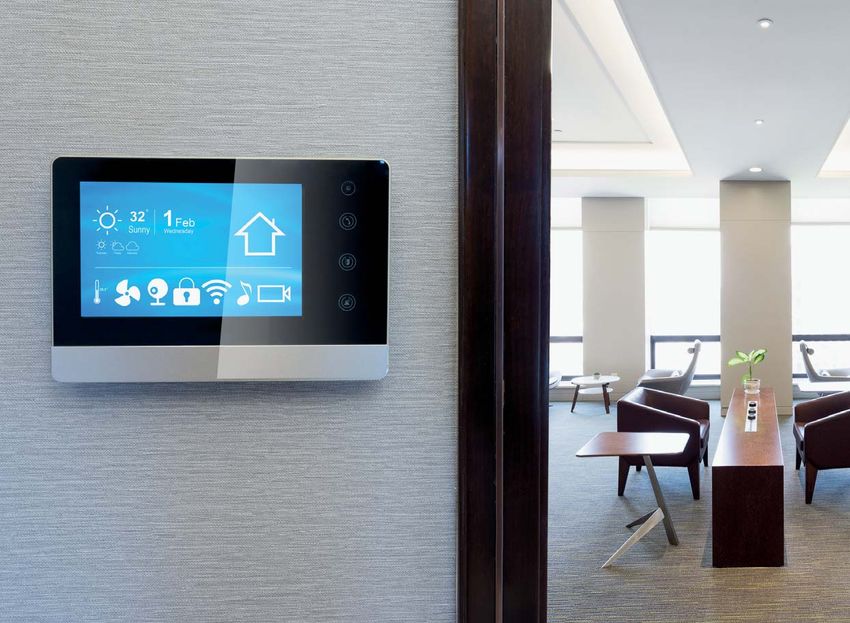
EDITORIAL | IMPULSE

»And the Quality                                                                                                              Editorial
Award goes to…«
Delivery reliability, service orienta-                                                              OUT OF THE BOX
tion, cooperation, flexibility, sustai-
nability and logistics performance -                                                                Dear readers,
these are the central criteria for the
                                                                                                    C
                                                                                                        ODICO is expanding! We are growing, and
evaluation of our suppliers.                                                                            the challenges for our logistics centre are
                                                                                                    also increasing; we need more space, and a

W
       e regard the regular evaluation of our sup-                                                  significantly higher level of automation. Yet the
       pliers as a proven means of determining                                                      purpose of our enlargements (see more on page
special services simply and meaningful. CODICO                                                      52) is not only to create additional space. We did,
is once again awarding the Quality Award to the                                                     however, provide for sufficient new space – in
best of over 150 suppliers this year.                                                               our enlarged office and logistics areas, and in our
                                                                                                    new recreational park.
The CODICO QUALITY AWARD
2018 was awarded to                                                                                 To continue our success into the future, we also
                                                                                                    intend to look into new working methods, and
 TOREX Semiconductor Europe Ltd.             96                                                     to examine the way we deal with the breathta-
 ASAHI KASEI MICRODEVICES Corporation        94                                                     king pace of the world of work, the constant time

 POWER INTEGRATIONS International, Ltd.      94
                                                                                    Sven Krumpel    pressure, the permanent multitasking, and the
                                                                                     CEO CODICO     resulting loss of motivation and a superficiality
 RUBYCON                                     93
                                                                                                    in our society. CODICO thus puts a significant
 CELAIN Technologies Enterprise Ltd.         92                                                     amount of effort in finding out how the company
                                                                                                    can think out of the box. How to create an envi-
 FCI Deutschland GmbH                        90
                                                                                                    ronment that fosters creativity, gives our staff
 SAGAMI                                      86
                                                                                                    enough space for development, the space we
 NIDEC COPAL Electronics GmbH                86                                                     require to find creative technical solutions for
                                                                                                    our customers.
Congratulations and many thanks to our sup-
pliers for their outstanding performance and                                                        Our expansion attempts to incorporate the latest
trustful cooperation!                                                                               findings in neuroscience, and to provide an ans-
                                             D01                                                    wer to the question »How do I create the best
                uPetra Huynh, +43 1 86305 169                                                       conditions to allow the human brain to work in
                        petra.huynh@codico.com                                                      the most efficient way possible.« The new space
                                                                                                    provides social areas and workbenches to allow
                                                                                                    joint work in groups and to encourage informal
                                                                                                    communication. We are implementing a Corpo-
                                                                                                    rate Farming Project: we will be cultivating fruits
                                                                                                    and vegetables, and we will build a recreational
                                                                                                    park with sports and fitness facilities for our
                                                                                                    employees and their families.

                                                                                                    The objective of our internal and external »reno-
                                                                                                    vation« – to be completed by late 2020 – is to pro-
                                                                                                    mote open-mindedness and alternative thinking.
                                                                                                    We see our growth not only as an opportunity to
                                                                                                    expand from a business point of view, but also
                                                                                                    as a chance to think out of the box and to encou-
                                                                                    Quality Award   rage boldness and individuality.
                                                     ©fotogestoeber - Fotolia.com

                                                                                                                                                  D02

                                                                                                                                     uSven Krumpel
                                                                                                                                               2019:1 | 3
IMPULSE | ACTIVE COMPONENTS

   SMART SPEAKER
   Build a »Smart« Bluetooth

                                                                                                                                                          ©lassedesignen - Fotolia.com
   Speaker with CSRA68105!
   Smart Speakers, or Speakers enabled to receive voice commands                                      resources. Generally the challenge for designing
   and act on those, are a very hot topic in the Audio market today and                               a Smart Speaker, and even more so a portable
   most companies in the Audio industry have some form of Smart Speaker                               Smart Speaker, is battery life and power con-
   in their product portfolios.                                                                       sumption.

   O
        ne of the design challenges companies      run and because of that also requires more         In the case of CSRA68105 QUALCOMM have set
        meet when designing a Smart speaker is     power. QUALCOMM do have these platforms,           their sights on minimal power consumption and
   that the platforms used are many times quite    and more to come when it comes to the High         hence uses the connection to the mobile phone
   complex and require an Operating System to be   End of the Smart Speakers, but here we will talk   for enabling the connectivity needed for the
                                                   about the lower end of the scale, where a design   Smart functionality. The CSRA68105 has enough
                                                   is less complex and can therefore use smaller      RAM memory to catch the phrase after a key-
                                                   more self contained SoC device running a Real      word and forward that in the stream for a cloud
                                                   Time Operating System (RTOS).                      based (ror even terminal based) voice service
                                                                                                      application to act on the information. What this
                                                   For RTOS-based speakers QUALCOMM can sup-          gives you as a developer and/or end customer
                                                   port voice enablement using the CSRA68105 SoC      is a product with a very streamlined power con-
                                                   – a high-performance, single-chip Bluetooth® au-   sumption and still the Smart functionality reque-
                                                   dio SoC, designed for premium wireless speaker     sted by most people looking to buy a Bluetooth®
                                                   and headphone applications. This highly integra-   enabled Speaker today.
                                                   ted SoC is engineered to include a comprehensi-
                                                   ve selection of connectivity, system processing,   There are several companies offering Voice Ser-
                                                   audio processing and power management              vices today, both for resolving voice commands

4 | 2019:1
ACTIVE COMPONENTS | IMPULSE

                                                                                                         of digital signal processor (DSP) processing power

                               CSRA68105                                                                 and advanced features on a single-chip RTOS
                                                                                                         platform. Dual 240MHz QUALCOMM® Kalimba™
              Bluetooth®        Developer DSP          IO & USB
                                   240MHz                                       USB/GPIOs                audio DSPs, and QUALCOMM® Kymera™ audio
                         ®
              Bluetooth                                                                                  framework offer more DSP processing power to
              Low Energy        Developer DSP         LED Drivers              LED/Buttons               eliminate the need for external audio processing
                                   240MHz
              Bluetooth®                                                                                 previously required to support premium features
                 Radio            Developer           Capacitive                                         such as far-field voice processing and advanced
                                  Application           Touch                  Analog Audio
              NFC Type II         Processor                                                              musical effects and reduces eBOM.
                 Tag               120MHz              Speaker
                                                      PWM (8-ch)               Digital Audio
                                    System
                                   Processor          HD Audio
                                                                                  Battery
                                                      class H HS

                                                       SMPS and
                                                                                  Sensors
                                                     Li-Ion Charger

                 XTAL                 FLASH                                                              CSRA68105 Devboard

                                                                                                         A more comprehensive listing of features and
                                                                                                         specifications.

and many also have their own look up services,       The technical features embedded in the CSRA         Features
control system interfaces etc. and with the open     68100 support OEMs in the development of pro-       • Powerful quad-core processor architecture
framework of the development system you as a         ducts with superior audio quality, voice control,   • Dedicated 120MHz 32-bit processor
developer can choose to work with the partner        far-field echo cancellation, sensor processing and    application subsystem
of choice that suits your particular needs.          audio post processing, raising the bar in terms     • Dual-core 240MHz Kalimba™ DSP Audio
                                                                                                          subsystem
                                                                                                         • DSPs support downloadable capabilities
        SPECIFICATIONS                                                                                    from RAM/QSPI and pre-installed library
                                                                                                          functions from ROM
  • CPU                                              • Audio Outputs: 2x high-quality line level DAC     • Further system processor with embedded
  • CPU Clock Speed: 2× 120MHz                        outputs, 2x low power Class-H headphone
                                                                                                          Bluetooth protocol stack
  • CPU Cores: System firmware processor, De-          drivers, 4x 24-bit I²S up to 192kHz, 4x 24-bit
                                                                                                         • Embedded ROM + RAM and external
    dicated customer application processor            SPDIF up to 192kHz, 8-ch PWM audio outputs
                                                                                                          QSPI Flash
  • DSP                                              • Charging
                                      ®
  • DSP Technology: 2× QUALCOMM Kalimba™             • Maximum Current: Up to 1.8 A                      • Variety of high definition audio interfaces
    DSP, QUALCOMM® Kymera™ DSP Framework             • Battery                                           • 2-ch 24-bit 109dBA line outputs
  • DSP Clock Speed: 2× 240 MHz                      • Battery Type: Li-ion battery                      • 2-ch 24-bit 100dBA line inputs
  • Bluetooth                                        • Memory                                            • 2-ch 24-bit 96dBA class-H ground referenced
  • Bluetooth Version: Bluetooth® 5.0                • Flash: Flexible QSPI Flash (external) program-     headphone driver
  • Class Support: Class 2, Class 1                   mable platform
                                                                                                         • 8-ch 108dBA PWM speaker outputs
  • NFC                                              • Interface
                                                                                                         • 4× 384kHz 24-bit I2S
  • Integrated NFC Radio: NFC type II, Peer-to-      • Supported Interfaces: USB device and host,
                                                                                                         • 4× 96kHz 24-bit SPDIF interfaces
    peer listener mode, Tag mode                      SDIO v3.0 host, I²C, SPI, UART
  • General Audio                                    • Input/Output                                      • Integrated Bluetooth® 5 and NFC tag radios
  • Audio Technology: QUALCOMM® Broadcast            • Summary: 2× audio line in, 2× audio line out,     • Dual-mode Bluetooth® BR/EDR and
    Audio Technology, QUALCOMM® aptX™ audio           2× microphone in, 2× headphone out, 4× I2S,         Bluetooth® Low Energy
    technology                                        PCM in/out, 4× SPDIF in/out, 8× audio PWM          • Pin-to-Pin compatible with CSRA68100
  • QUALCOMM® aptX™ playback support: aptX            out, UART, USB, I²C/SPI, 13× XI                    • Advanced power management with
    Classic, aptX HD, QUALCOMM® eXtension pro-       • ADC: 2-ch 100dBA 24-bit ADC with micro-
                                                                                                          integrated SMPS & Li-Ion battery charger
    gram                                              phone pre-amp, 8-96kHz sample rates
                                                                                                          with USB type-C charger support
  • Digital Microphone Input: Up to 8 digital mics   • General Purpose IOs: 63
                                                     • DAC: 2-ch 109dBA 24-bit DAC, 8-192kHz sam-        • Rich array of interfaces including LED
  • Audio Inputs: 2× high-quality line level ADCs,
    2× low power ADC, 4× 24-bit I²S up to 192kHz      ple rates                                           drivers and capacitive touch
    with programmable MCLK, 4× 24-bit SPDIF                                                                                                           A01

    up to 192kHz                                                                                                          u   Johan Wesslén, +46705679770
                                                                                                                                johan.wesslen@codico.com

                                                                                                                                                   2019:1 | 5
IMPULSE | ACTIVE COMPONENTS

   Author: Miriam Leunissen, EOS

  CUSTOMISATION
  ON A SOUND BASIS
   CODICO and two international medium-sized firms demonstrate how
   modified standard power supply solutions in medical technology can work!

                                                                                                                    ons, EMC, and the load profile. »This time again,
                                                                                                                    it proved indispensable to implement a multitude
                                                                                                                    of adjustments. Therefore, we were very glad to have
                                                                                                                    CODICO as distribution partner and EOS Power as
                                                                                                                    manufacturer of the said power supplies on board
                                                                                                                    again during the development of this new generati-
                                                                                                                    on of our prisma VENT ventilators.«

                                                                                                                    What followed was by no means a walk in the
                                                                                                                    park: as a result of the new medical classification
                                                                                                                    and the sensors used by Löwenstein, which are
                                                                                                                    built in the latest generation of breathing masks,
                                                                                                                    the standard prescribes that the connection bet-
                                                                                                                    ween the patient and the device must be consi-
                                                                                                                    dered conductive. Therefore, the otherwise insu-
                                                                                                                    lated section now had to meet BF, 2×MOPP, and
                                                                                                                    protection class II requirements. The fact the new
                                                                                                                    EOS (M)WLP225 series to be used in this case
                                                                                                                    had been approved – just as all other EOS series –
   At first, it seemed that the prisma VENT50 ventilator                                                             according to the relevant EMC standards EN
   by Löwenstein Medical Technology was heading for a                                                               60601, 3rd and 4th edition provided a solid ba-
   quick open-frame power supply solution.                                                                          sis.

   O
         n offer was a small power supply measu-           »made in Hamburg« ventilators, more precisely             »Of course, we also very much welcomed the fact
         ring just 2×4×1 inches, with a 28W output        than any other open frame power supply unit               that, in addition to the approval background and
   per cubic inch, convection cooling up to 112.5W,       available in the market. Moreover, according to           the compact size, the price of the EOS open frame
   and 225W with forced ventilation. In addition, a       the unanimous opinion of all project managers,            power supplies was also very reasonable«, says
   dual input fuse, a standby power consumption           the device performed to datasheet specifications           Heinrich. »Because ultimately, all these series of
   less than 0.5W, and an MTBF of over 3.3 million        during intensive pre-tests.                               ventilators we are talking about are price-sensitive
   hours. The efficiency factor of up to 94 percent                                                                   home ventilation devices, for which price and quality
   was okay, the temperature shut-off and start gua-       Yet the »power supply for prisma VENT50« pro-             must be brought into balance.« But this was not
   rantee for as low as -40°C were in line with the       ject was far from being a slam dunk. »As so often         the sole criterion for our decision. As with the
   specifications. According to the CB report, all out-    the case in medical technology, the devil is in the de-   simpler predecessor model prisma VENT30/40,
   put voltages from 12V to 58V were approved.            tail«, recalls Wolfram Heinrich, who has been part        and in the case of the VENTIlogic LS ventilation
                                                          of the prisma VENT development team for many              device, which are both already equipped with
   All this came in a medical class II design for devi-   years and the Electronic New Device Division pro-         the older EOS MWLT 150 power supply unit,
   ces with direct body contact, and it conformed         ject manager since 2014, thus also in charge of           the Löwenstein team deliberately opted again
   to the demands of the development department           sampling for the Prisma VENT ventilator series            for an EOS Power open frame power supply
   at Löwenstein for their new series of high-quality     at Löwenstein. The main topics were connecti-             from CODICO.

6 | 2019:1
ACTIVE COMPONENTS | IMPULSE

Make or Buy
Already at that time, the crucial »make or buy«
question was almost reluctantly decided in fa-
vour of »make«. For a short while, the developer
team of the respiratory device was overwhelmed
by the feeling that they were trying to square the
circle, because all the usual, affordable off-the-
rack standard units were out of the question.

This is a feeling many developers in medical tech-
nology are all too familiar with. »Today, there are
only a few power supply unit makers who offer the
class II medical technology standard as an open
frame standard device; at the time, there was prac-
tically none. Our device, however, had to remain af-
fordable for the end customer - and still be small,
lightweight, and safe«, as Heinrich remembers the
situation eight years ago, when his Hamburg              Manfred Schulz (CODICO) with Wolfram Heinrich (Löwenstein)
branch still operated under the name »Wein-
mann«.
                                                        had already been modified according to the cus-        can be traced seamlessly from the end customer
In its MWLT version, the WLT150 by EOS was one          tomer’s specifications in an earlier stage of the      back to the pre-supplier, including all component
of the few power supply units at the time that          cooperation – including the heat shrink tube, for     suppliers involved.
already had a class II certification; since the 3rd      fire protection reasons.
edition of the EN60601, it is available with upgra-                                                           More than just new connectors
ded specs and also features 2×Y2 capacitors for         Issue number two: goods receipt, workflow, and         From a technical point of view, changes did not
2×MOPP. It was recommended by Austrian dis-             traceability. Since 2016, in the areas of goods re-   merely include the usual standard modifications
tributor CODICO, with whom Löwenstein had               ceipt, production, quality assurance, and batch       from the connector to the output voltage, but al-
already successfully cooperated for several years       control, Löwenstein has been working with spe-        so involved in-depth profile adjustments. When
in the area of displays and components. Those           cial barcode labels required on the components        it became evident that the ordinary voltage and
in charge jointly decided to give it a try with a       in triplicate at the production in Hamburg. These     load profiles of the Löwenstein devices did not
clever modification of the WLT150, if possible          labels, including the barcode and the peel-off        exactly meet the standard profiles of the EOS de-
without affecting the certification-related para-         sticker, are already affixed and registered at the      vices, components were added and modified at
meters. »In the times that followed, our people and     manufacturer in Mumbai. Measures were also            several points following intensive joint test series
the European sales agents of EOS could have just        taken with the support of CODICO in India to          in Hamburg and Mumbai.
as well set up office at Löwenstein in Hamburg, still     meet customer-specific ESD packaging require-
Weinmann at the time«, says Manfred Schulz, FSE         ments. In the unlikely event of a necessary recall,   For instance, Ventilogic LS was fitted with an
Active Components at CODICO, summing up the             e.g. in case of a higher failure rate, the product    NTC for temperature monitoring and ventilator
intense cooperation between the three medium-
sized firms.

Issue number one: the connections. EOS Power
often supplies its customers with special connec-
tors from its factory in Mumbai. Depending on
the requirements, the user can choose between
screw and plug-in type terminals at the output.
A special output connector was chosen for the
Löwenstein power module. As a result, the device
manufacturer can work with the same cable har-
ness in all its devices. In addition, the positioning
holes and the cross section of the mounting and
the circuit board for the ventilation device were
individually adjusted in several small steps. In ad-
dition to the connections, seemingly trivial things

                                                                                                                                                          2019:1 | 7
IMPULSE | ACTIVE COMPONENTS

                                                                                                                ment and production. As a result, they managed
                                                                                                                to overcome quite a few challenges together, ran-
                                                                                                                ging from strange noises coming from the device
                                                                                                                after a long standby, to overheating capacitors.
                                                                                                                Since the handling of critical components is
                                                                                                                a key part of risk analysis within the meaning
                                                                                                                of EN60601, assembly versions and second-,
                                                                                                                third-, and fourth-source components pose ma-
                                                                                                                jor challenges for all medical technology manu-
                                                                                                                facturers. Therefore, customer-specific adjust-
                                                                                                                ments would be almost impossible without an
                                                                                                                open approach to the parts list.

                                                                                                                Ideal conditions for
                                                                                                                high mix/low volume
                                                                                                                Another advantage was the fact that all EOS
   control as requested by the customer, due to ven-     Löwenstein team, however, the required re-cer-         power supplies are manufactured centrally at
   tilation phases with very high outputs. In additi-    tification following the replacement of compo-          EOS Power in Mumbai. The manufacturing instal-
   on, different MOSFETS that can cope with parti-        nents was done quickly and without any difficul-         lations are intentionally flexible and geared to a
   cularly high voltages were used in the PFC stage      ties. At around 5,000 dollars, the costs were si-      high mix and a wide variety of modifications, so
   in the Ventilogic LS. Subsequently, the 2×Y2 ca-      gnificantly lower than the costs for a new certifi-      that volumes of just a few thousand identical
   pacitors were also adjusted to improve the load       cation of a power module, which can easily reach       components each year can be produced there
   profiles and EMC performance. This close deve-         more than double that amount.                          cost-efficiently. These high-mix/low-volume »pick-
   lopment cooperation only worked because a pro-                                                               and-place« systems can handle different types
   totype of each modified ventilation device was         Behind-the-scenes                                      of circuit boards and components. For instance,
   sent to EOS Power in India for measurements.          process integration                                    the designs have different connectors to cope
   The renewed EMC measurements (incl. surge             »The integration of processes behind the scenes also   with the compact size of the power supplies; the
   and burst) were also carried out in parallel both     suits us«, stresses Wolfram Heinrich of Löwen-         facilities ensure a reliable positioning of large
   in Germany and India.                                 stein. In addition to the modifications on the part     components and the mounting of resistors and
                                                         of the manufacturer, CODICO operates a seam-           tiny capacitors – as well as the exact placement
   As a whole, however, all the modifications in         less serial-number tracking and customer-speci-        of a wide range of SMT components down to fine-
   the MWLP225 did ultimately result in the need         fic packaging labelling system, and the producers       pitch parts such as ICs, QFN packages and BGAs.
   for additional certification for the modified         in India perform additional DoC tests. These
   MWLP225, because critical components and              are documented accordingly. As a result, an ad-        The manufacturing site has received numerous
   safety-related barriers had been altered. Sanjay      ditional quality requirement of Löwenstein was         quality and manufacturing awards from reputa-
   Pusalkar, Head of Engineering at EOS Power:           efficiently solved in the cooperation group.           ble bodies like Dun & Bradstreet, Frost & Sullivan
   »When the separation between patient and current                                                             or Elcina. The manufacturer Löwenstein Medical
   flow changes, or when optocouplers and parts in        For the best possible implementation of innova-        Technology (still Weinmann at the time) also au-
   charge of monitoring control are modified, re-certi-   tions, EOS Power and CODICO supported his              dited the EOS production in India years ago and
   fication becomes obligatory.« According to the        company with its documentation obligations to          approved it following a few supplementary agree-
                                                         an extent that goes beyond usual market practi-        ments.
                                                         ce, as Löwenstein Project Manager Heinrich em-
                                                         phasizes. According to Heinrich, EOS provided al-      The successful cooperation between the three
                                                         most 40 datasheets of capacitors and other com-        international companies is currently entering its
                                                         ponents. Circuit diagrams as well. »This is really     third round. The product is still top secret, but
                                                         an extraordinary service and support«, Heinrich as-    this much can be revealed: CODICO visited
                                                         sures. He believes the reason lies in the »similar     Löwenstein more than a dozen times during the
                                                         corporate culture and customer focus« of the three     last two years, and the responsible product ma-
                                                         partners. This is what helped their collaboration      nager of EOS flew over to Europe equally often.
                                                         succeed even in time of difficulties, and despite
                                                         the large distances.                                   For further questions, please contact:
                                                                                                                                                             A02

                                                         The group takes an equally open approach to ad-                  u   Andreas Hanausek, +43 186305 131
                                                         dressing problems in the early stages of develop-                        andreas.hanausek@codico.com

8 | 2019:1
ACTIVE COMPONENTS | IMPULSE

                            POWER MANAGEMENT
                            Solutions for small FPGAs & MCUs!
©Viacheslav - Fotolia.com

                            Realizing Power Sequencing and High-Speed Transient                                                               Using a PMIC is today the most standard solution
                            Response without a PMIC!                                                                                          for providing the power to the multiple rails re-
                                                                                                                                              quired by small FPGAs. However, using a PMIC

                            S
                                mall Field-Programmable Gate Arrays                    Core voltage is normally 1.2V or 1.0V. DDR me-         also has its own problems including how to make
                                (FPGAs) are extremely common today in                  mory needs typically 1.5V or 1.8V and I/Os need        effective sequencing, probable unstable operati-
                            digital designs and many FPGA applications usu-            2.8V or 3.3V (refer to Figure 1 below).                on and EMI issues caused by long wiring from
                            ally require multiple voltage rails to power them.                                                                the PMIC to the FPGA as well as the influence of
                                                                                                                                              a common GND and finally, there are thermal
                                                                                                                                              considerations to be considered with a PMIC
                                                                                                                                              solution due to the concentration of heat in one
                               12/24V                           5.0V                                                                          place.
                                                                                                                   3.3V I/0
                                           Primary DC/DC                                   DC/DC
                                                                                                    CE
                                                                                                                                              Power Sequencing
                                                                                                                                 FPGA / MCU

                                                                                                                                              In addition to the specific power rails listed above,
                                                                                                    PG             1.8V DDR                   the different voltages must be powered on and
                                                                                           DC/DC
                                                                                                                                              perhaps more importantly, but often overlooked,
                                                                                                    CE
                                                                                                                                              powered off, in the correct order to maintain
                                                                                                                                              system stability. This is known as »power sequen-
                                                                                                    PG             1.2V Core
                                                                                           DC/DC                                              cing« and for start-up will usually begin with the
                                                                                                                                              Core voltage and, depending on the FPGA, will
                                                                                                                                              end with the I/O voltage. For power off the order
                             Figure 1: Power Configuration of Conventional FPGA & MCU                                                          is usually the opposite so I/O off first and Core

                                                                                                                                                                                          2019:1 | 9
IMPULSE | ACTIVE COMPONENTS
The power sequence of start-up and shutdown
of the 3 rails is important as already highlighted
12/24V 5.0V
Primary XCL, DC/DC 3.3V I/0
ENABLE and it can actually be realized by a simple RC de-
DC/DC ex. XCL219
PG CE lay for the CE pins of each DC/DC (Figure 6 & 7).
FPGA / MCU
A RESET IC (TOREX XC6126C) that monitors the
RESET XCL, DC/DC 1.8V DDR
XC6126C ex. XCL219 VIN voltage is recommended for the ENABLE
CE
signal driving RC. Without the RESET IC, the
sequence may be unreliable, or the VIN start-up
XCL, DC/DC 1.2V Core waveform may be limited. Please note that if the
ex. XCL219 primary side DC/DC has PG (Power Good) as
CE
shown in Figure 2, the ENABLE signal can be
Figure 2: Power Structure for FPGAs & MCUs with RESET IC
driven by the PG signal. In addition, it should also
be noted that if the voltage from the output of
voltage off last. Seems simple enough but there make the power on sequence and therefore it is the primary side DC/DC is 3.3V a line switch (such
are pitfalls if it isn’t done properly and to do quite common to have a Power Good (PG) out- as the TOREX XC8107) should be used instead of
on/off sequencing properly usually means ad- put which is used to provide an Enable signal to a Micro DC/DC or DC/DC.
ding a large and expensive capacitor on the Core next DC/DC in the sequence and so on (as shown
voltage rail to make sure that it stays on until all in Figure 1). TOREX Power ICs suitable
the other rails are powered off in the right order for use with small FPGAs & MCUs
during power down. TOREX has a solution, however, that will enable For stable FPGA and MCU operation, it is impor-
the sequencing to be done without a PMIC and tant that each DC/DC is positioned at the
Typical Power without the need for a large and expensive Point of Load (POL) as that reduces impedance
Sequencing Requirements Capacitor on the Core voltage rail. Read on! between the DC/DC and the FPGA or MCU. It
As mentioned, to have a secure shutdown se- is equally important to separate each heat
quence (power off), the 1.2V Core voltage should Point of Load (POL) method with source and to layout the PCB to reduce EMI and
be maintained until all the other rails are off, so TOREX Micro DC/DCs (integrated to avoid interference between each power sup-
a large (>2,000μF) and expensive Capacitor is ne- Coil) & Hi-SAT COT DC/DCs ply. The XCL Micro DC/DC series with integrated
cessary for the Core rail. When the 5V rail is off, POL with TOREX’s XCL Micro DC/DCs and/or Hi- coil is ideal for FPGA power supply use because
the UVLO of each secondary DC/DC operates and SAT COT solutions realizes a very stable operati- they have low EMI, good thermal characteristics,
cuts off their outputs but the large capacitor of on, fast transient response, good dispersion of are simple to design with and are very small
the Core rail is used to keep its voltage until all heat and lower EMI thereby solving all the issues (Figure 3 & 4).
other rails are powered down. normally associated with powering FPGAs and
power sequencing. The advantage of using indi- In addition, the core voltage (which is normally
Because of the large capacitor, it is also difficult vidual ICs rather than a PMIC is that each IC can 1.2V or lower) requires high accuracy and fast
to control the rise-up time of the Core rail to be located closer to each pin on the FPGA (POL). transient response so here TOREX DC/DC &
Hi-SAT COT Buck DC/DC vs PWM/PFM Buck DC/DC
VIN = 3.6V, VOUT = 1.8V, TRISE = TFALL = 2μs, TA = 25ºC,
Hi-SAT COT Buck DC/DC: CIN = CL = 10μF (ceramic)
PWM/PFM Buck DC/DC: CIN = 4.7μF (ceramic), CL = 10μF (ceramic)
1.90 3.0 1.90 3.0
1.85 20µs 2.5 1.85 60mV 2.5
Output Voltage: VOUT [V]
Output Voltage: VOUT [V]
Output Current: IOUT [A]
Output Current: IOUT [A]
Figure 3: Pocket Style Micro DC/DC with 260µs
integrated Inductor for IOUTS up to 1A 20mV
1.80 2.0 1.80 2.0
20mV 380µs
1.75 1.5 1.75 1.5
20µs
90mV
1.70 1.0 1.70 1.0
VOUT (Hi-SAT COT)
VOUT (PWM/PFM)
1.65 0.5 1.65 IOUT 0.5
1.60 0 1.60 0
Time [100μs/div] Time [100μs/div]
Figure 4: Multiple Style Micro DC/DC with
integrated Inductor for IOUTS >1A Figure 5: Load Transient Performance Comparison between Hi-SAT COT & Standard DC/DC
10 | 2019:1ACTIVE COMPONENTS | IMPULSE
Micro DC/DC solutions that support Hi-SAT COT
control (Fig.5) such as the XC9257 or XCL219 (1A)
and the XC9260 or XCL213 (1.5A) are suitable.
Power Sequencing & High-Speed
TOREX Solutions for small
Transient Response without PMIC!
FPGAs & MCUs (VIN=5.0V & VIN=3.3V)
With a 5.0V input, a 4.0V CMOS output RESET IC
such as the TOREX XC6126C40A7R-G is recom-
mended to make the ENABLE signal whereas
with a 3.3V input, a 2.4V solution is suitable,
XC6126C24A7R-G. If the ENABLE is connected di-
rectly to VIN without a RESET IC, VIN must rise-up
©Viacheslav - Fotolia.com
faster than the RC delays and the shutdown se-
quence will not be realised because each power
IC will turn off when the VIN reaches the IC’s UV-
Buck DC/DC
VIN = 5.0V
VIN VOUT 3.3V Condition
CIN33 1.0A VIN : 5V
XCL219B333FR-G ENABLE Sig. : H = 5V, L = 0V
ENABLE SD33 XC9257B33CER-G CL33 Startup* : 1.0V 1.8V 3.3V
Shutdown* : 3.3V 1.8V 1.0V
CE
RD33 *Sequence
CD33 Buck DC/DC Solution
FPGA / MCU
3.3V 1.0A
VIN VOUT 1.8V
XCL219B333FR-G
CIN18 1.0A
XCL219B183FR-G XC9257B33CER-G
XC9257B18CER-G CL18 RD33: 120kΩ, CD33: 0.1μF
XBS013R1DR-G
CE 1.8V 1.0A
RD18
XCL219B183FR-G
CD18 XC9257B18CER-G
Buck DC/DC
RD18: 64kΩ, CD18: 0.1μF
VIN VOUT 1.0V 1.0V 1.5A
CIN10 1.5A XCL213B103DR
XCL213B103DR
SD10 XC9260B10CER-G
XC9260B10CER-G CL10 RD10: 100kΩ, CD10: 0.1μF
CE XBS013R1DR-G
LO voltage. If the primary DC/DC for 12/24V input
RD10
has a PG pin, please use it for the ENABLE signal.
CD10
Figure 6: TOREX Solution for Powering FPGAs/MCUs when VIN =5.0V
In both cases (VIN=3.3V & VIN=5.0V), the power
sequence can be realised using just a RC delay
for each CE pin without the need for a dedicated
Line Switch
VIN = 3.3V PMIC, multiple RESET ICs or the large capacitor
VIN VOUT 3.3V Condition
CIN33 1.0A VIN : 3.3V on the Core voltage rail highlighted earlier. A
ENABLE XC8107AC10ER-G ENABLE Sig. : H = 3.3V, L = 0V
SD33
CL33 Startup* : 1.0V 1.8V 3.3V simpler solution with the added benefits of lower
Shutdown* : 3.3V 1.8V 1.0V
CE EMI and better thermal performance!
RD33 *Sequence
CD33 Buck DC/DC Solution
Samples and/or evaluation boards for all the
FPGA / MCU
3.3V 1.0A
VIN VOUT 1.8V
XC8107AC10ER-G TOREX products mentioned in this feature can
CIN18 1.0A
XCL219B183FR-G RD33: 64kΩ, CD33: 0.1μF,
XC9257B18CER-G CL18 SD33: XBS013R1DR-G be requested via CODICO. The evaluation boards
1.8V 1.0A
CE are made to the customer’s specific require-
RD18 XCL219B183FR-G
XC9257B18CER-G ments. Test data is provided with each board. In
CD18 RD18: 64kΩ, CD18: 0.1μF
Buck DC/DC addition, TOREX can also provide solutions for
1.0V 1.5A
VIN VOUT 1.0V XCL213B103DR the Primary step-down DC/DC from 12V/24V so
CIN10 1.5A XC9260B10CER-G
XCL213B103DR
SD10 RD10: 100kΩ, CD10: 0.1μF, please ask your local CODICO contact for details.
XC9260B10CER-G CL10 SD10: XBS013R1DR-G
CE
RD10 A03
CD10
u Johannes Kornfehl, +43 1 86305 149
Figure 7: TOREX Solution for Powering FPGAs/MCUs when VIN =3.3V johannes.kornfehl@codico.com
2019:1 | 11IMPULSE | ACTIVE COMPONENTS
EMBEDDED LCD
WITH INTELLIGENCE
©Sergey Nivens - Fotolia.com
Nowadays, it is inconceivable to have any applications without colour with brightness adjustable in 64 steps. The me-
displays. Although a monochrome variant would often fulfil the mory for the firmware is provided by an SD card.
purpose as well, in most cases the colour variant is given preference, And, of course, the series has an operating tem-
simply as a demonstration of modern concept and approach. Mono- perature range suitable for industrial uses, from
chrome displays are easy to handle, because they require a lower data -20°C to +70°C. Interactivity is achieved by way
volume than a colour display. of a resistive touchpanel.
B
ut it is not always the case with an applicati- then loaded into the Embedded LCD hardware. When getting started, help is provided by a set
on that a CPU is available with sufficient ca- consisting of embedded LCD, AC/DC adapter,
pacity to provide a colour display with a higher What advantages does USB/UART adapter board, mini-USB cable and
resolution. If it is intended that a display should this solution provide? FFC (Flexible Flat Cable), which is available for the
be located at a considerable distance from a • The integrated embedded CPU allows for individual sizes. The display is connected to a PC
computer, then consideration also needs to be rapid reaction times, and has low current by way of the USB adapter board. This means
given as to how to control the display. Not having consumption. that commands are sent to the panel, and, in the
a suitable computer on the spot, in other words • The graphic development environment allows opposite direction, data is received from there.
directly at the display, means having long con- for fast & flexible working, and is easy to use. Communication from and to the host takes place
necting lines, and that in turn can cause pro- • The UART interface can be easily integrated in real time.
blems with data transfer. into existing systems.
• Products can be developed quickly and What about the software?
How to tackle the challenge? swiftly brought onto the market. OGUS is a graphic development environment,
ORIENT DISPLAY offers a possible answer • The system provides high reliability & stability. which makes working with Embedded LCD’s con-
here, and one that is easy to use – the Embed- siderably easier. With the aid of the software,
ded LCD. The solution consists of a hardware What hardware is touch functions and display activities are defined
part and software part. The hardware is made available at present? and the configuration and the user interface pro-
up of the display itself and an embedded micro- The AGN Series at the moment consists of three grammed. After completion, the project files are
processor, including the peripherals, with the display sizes – 3.5“ with a resolution of 320×240 adopted into the Embedded LCD by way of SD
PCB located on the rear of the display. The soft- pixels, 4.3“ with 480×272 pixels, and 7.0“ with card. This method also makes series production
ware part is the development environment 800×480 pixels. The displays have a UART inter- easier, and also simplifies updates which may
known as OGUS (Orient Graphic Utility Software). face, by means of which the commands are sent be necessary. The structure of the OGUS deve-
This is where the project files are generated, and to the displays. This supports 65,536 colours, lopment software is represented in Picture 1.
12 | 2019:1ACTIVE COMPONENTS | IMPULSE
SOFTWARE SOFTWARE
Development materials
Font Library file, Icon Library file, Interface Picture file • Each picture is broken down into a
number of control elements, and the
OGUS Software, Interface Function, Configuration & Development
user can extend the configuration file
13.bin 14.bin 22.bin config.txt simply by adding an element.
touch/keying variable variable hardware
Configure File Configure File Initialize File Configure File • There are a large number of control
elements to choose from, such as data
SD Card download input, touch input, audio reproduction,
etc.
• Readily available are 56k RAM, 8 me-
mory channels for data curves, and fast
HARDWARE
TFT Display Variable Storage Curve buffer Register Interface
Interface: 56KB Interface Hardware processing of the variables in maximal
Display variable 8 Channels, Interface &
& format control 8 Curves Process Control 80ms.
Text Display 0x82 W
0x83 R
0x80 W
0x81 R
• There are 256-byte configuration regi-
Icon Display
Graph Display Touch Panel UART Interface: 8N1 Mode, customizable sters for the hardware control. These
Baud Rate up to 1Mbps, customizable
0x84 W Frame Header & optional CRC16 can be written & read via the interface.
• Each page can contain up to 128 dis-
play control elements and any desired
Picture 1: Structure of the OGUS development software
number of touch elements.
• Functions such as Real Time Clock (RTC),
backlight control, and capacitive touch
Aids such as font libraries, icon libraries, and pic- What are the benefits? panel, are easy to integrate.
tures are combined, and from these the configu- By contrast with conventional LCDs (without em- • User-defined databanks are supported.
ration files generated. Everything is stored on an bedded controllers) to which the data that is to • Mathematical functions (MAC, CRC,etc.)
SD card and transferred to the Embedded LCD. be displayed is transferred directly from the host can be implemented. Data storage, se-
There the data is copied into the Flash or RAM with specific timings, Embedded LCDs work on rial communications. and protocol pro-
cessing (such as Modbus) are no pro-
and implemented. Picture 2 shows the data flow the principle of direct variable processing. All ope-
blem either.
for the Embedded LCD. rations are carried out by comparison with pre-
defined variables. This makes work during the
Host Machine UART Display Screen development considerably easier.
Embedded Let’s assume we want to produce a thermostat
Download LCD Input which displays a temperature in real time, and
SD Card Touch Operation
Flash/RAM
by touch input switches to another page on
Project
j which parameters can be input. Picture 3 shows
Files
the conventional development layout in compa-
OGUS rison with the OGUS. It can clearly be seen that
Picture 2: Data flow for the Embedded LCD the process can be designed to be substantially
simpler.
Traditional LCM Development Flow OGUS Development Flow
So to sum it up: Even small controllers can be fit-
Convert Temperature Switch to Write Temperature Data
Data to ASCII Character Main Page to Variable Storage
ted with a colour display, and without losing any
(command 0x82) capacity for the tasks they are actually intended
Display ASCII
Character Save Setting Data to do. This means that the application or the
after Input
Write Temperature Data device can be provided with a display of much
Generate wiring to Curve Buffer
Coordinates (command 0x84) higher quality. Decentralised display units are
Display Input
ASCII easy to set up with embedded displays. Thanks
Shift Curve
Display Window Read Setting Parameter to operation via a serial interface, long connecti-
Convert Input ASCII to from Variable Storage
Setting Data (command 0x84) on lines with the use of RS232 or RS422 are no
Connect
new Coordinates problems at all. And that means the scope of
Handle the Input Process application for higher quality LCDs is widened as
Any touch based on the Button Value
Operations? N well.
A04
Calculate Button Display
Coordinates Buttons Picture 3: Conventional development uChristian Forthuber, +43 1 86305 158
layout in comparison with the OGUS christian.forthuber@codico.com
2019:1 | 13IMPULSE | ACTIVE COMPONENTS
©Viacheslav - Fotolia.com
T
his article illustrates the procedure of desi-
PASSIVE FILTER gning filtering to achieve ultra-low output
voltage noise of SMPS regulators. Single stage
capacitive filter is commonly used for DC/DC con-
verter applications. Low-ESR ceramic capacitors
DESIGN ©Viacheslav Iakobchuk - Fotolia.com
are utilized to meet output voltage ripple speci-
fications. The single stage capacitive filter is suffi-
cient for applications that requires no less than
1-2mV output voltage ripple. For applications
such as RF ADC and DAC applications where it is
Buck Regulators for
necessary to meet less than 1mV ripple, a second
stage LC filter should be used to effectively sup-
Ultra-low Noise Applications press the switching noise.
Single Stage Filter Design
A synchronous buck converter consists of an
Switched-mode power supply (SMPS) has the advantage of high input capacitor CIN, two switches S1 and S2 with
efficiency compared to traditional Low-dropout (LDO) regulators. their body diodes, an energy storage power in-
Due to its switching nature, a SMPS emits noise at its switching ductor L, and output capacitors, COUT. The input
frequency and its harmonics. source provides energy to the power inductor L
and the load when S1 is turned on and S2 is tur-
ned off. During this period, the inductor current
IL rises. The energy stored in the inductor is trans-
IOUT ferred to the output capacitor and load when S2
IL,p-p is on and S1 is off, causing the inductor current
to drop. The switching behavior of the buck re-
tON T gulator causes the output voltage to fluctuate.
VIN S1 VOUT The output capacitors COUT is placed at the out-
IL L IOUT put to smooth the output voltage under steady
IL,p-p/2
state. The output capacitor reduces the output
IC
IC T voltage ripple by providing a low impedance path
CIN S2 COUT tON for the high-frequency voltage components to
Control
IL,p-p/2 return to ground.
In the subsequent development, it is assumed
the buck converter operates under continuous
GND GND
conduction mode (CCM) for output voltage ripple
Figure 1: CCM operation of synchronous buck regulator minimization. The inductance of L is designed
14 | 2019:1ACTIVE COMPONENTS | IMPULSE
the power converter design is shown in Figure 2.
GND Plane In the PCB layout of MPM3833C, wide copper pla-
MPM3833C ne is used for the output power path to minimize
power losses. The output capacitors are placed
5 along the output current path. As shown in the
figure, as more capacitors are placed on the out-
VOUT Plane put plane, the distance from the additional capa-
citor to the output pin of the power module in-
creases. Consequently, more parasitic inductan-
VIN Plane
ce is involved in the output capacitor that is furt-
LOAD her away from the power module.
Adding more output capacitance become less
and less effective and eventually, the shunt loop
GND Plane
is dominant by parasitic inductance. To demon-
strate the impact of loop parasitic inductance, an
Figure 2: Typical PCB layout for MPM3833C power module
MPM3833C with various output capacitors are
simulated using Simplis. It is assumed that each
to meet inductor current ripple requirement. Where T is the period of one switching cycle. By additional output capacitor introduces an addi-
The minimum inductance of L is determined as: definition, the capacitor charge in a given period tional 0.5nH parasitic inductance to the bypas-
is also can also be expressed as: sing loop. Figure 3 illustrate the output ripple of
the power module with one 22uF capacitor. The
bypassing capacitor effectively reduces the out-
Where VIN and VOUT represent the input and out- put ripple to around 3mV at 5V input, 1.2V out-
put voltage, respectively, represents the Equating equations (2) and (3), the minimum ca- put, and 2A load.
duty ratio, IL,p–p is the peak-to-peak current ripple pacitance to achieve the required output peak-
of the inductor, and fsw epresents the switching to-peak voltage ripple, V(OUT,p–p) is determined as: To further reduce the output voltage ripple, 1 ad-
frequency of the converter. Typically, the peak- ditional 22uF output capacitors is place at the
4 IL,p–p
to-peak inductor current ripple is selected as 20- CMin = output. Since the new capacitor has to be placed
8fsw ΔVC,p–p
40% of the output DC current. further away from the power module, the para-
Ideally, the noise shunt capability can be increa- sitic inductance involved with the new capacitors
The output capacitance is selected to ensure that sed by paralleling more output capacitors. In is 1nH. The simulated output voltage ripple is
the output ripple is below the specified peak-to- practical, the output capacitors are laterally pla- shown in Figure 4A where the output voltage
peak value. For a single stage capacitive filter, an ced on a PCB. Adding more output capacitors on ripple is reduced to 2mV. Compared to the
minimum output voltage ripple of 1mV to 2mV a PCB would introduce additional parasitic induc- waveform shown in Figure 3, where one 22uF
can be achieved. Under steady state, the net elec- tance and AC resistance to the shunt path and output capacitor effectively brings down the out-
tric charge delivered to the capacitor is zero thus reduce the effectiveness of bypassing the put voltage ripple to 3mV, the additional one
within one switching period. The capacitor char- switching noise. 22uF capacitor is less effective. Figure 4B shows
ge of the shaded area in Figure 1 is calculated as: the output voltage ripple with one more 22uF ca-
A typical PCB layout of a MPS power module pacitor (total of 4×22uF). The last 22uF capacitor
which integrates optimized inductors to simplify involves 1.5nH parasitic inductance in its bypas-
1.2 1.2 A 1.2 B
U1-OUT / V
U1-OUT / V
U1-OUT / V
1.198 1.198 1.198
1.196 1.196 1.196
1.194 1.194 1.194
1.192 1.192 1.192
1.19 1.19 1.19
0 0.5 1 1.5 2 2.5 3 3.5 0 0.5 1 1.5 2 2.5 3 3.5 0 0.5 1 1.5 2 2.5 3 3.5
Time/uSecs 500nSecs/div Time/uSecs 500nSecs/div Time/uSecs 500nSecs/div
Figure 3: Output voltage ripple of MPM3833C Figure 4: Output voltage ripple of MPM3833C with
with one 22uF output capacitor (A) 4x22uF output capacitors and (B) 5x22uF output capacitors
2019:1 | 15IMPULSE | ACTIVE COMPONENTS
sing loop. As shown in the figure, the output ripp- Once the first stage capacitor COUT is determined quency. The attenuation at given frequency can
le reduction achieved by the additional 22uF and the specified output voltage ripple (at given be estimated as
capacitor is less than 5% compared to the case frequency) is given, the required attenuation of
8 (
where 3×22uF is used. the second stage LC filter can be determined as: A (f) = –40log ( f
f0 dB
5 VO,p–p
As demonstrated in Figure 3 and 4, the parasitic A0,dB = 20log Using the attenuation calculated in equation (5),
V1,p–p
inductance introduced by the PCB copper/trace the required cut-off frequency is determined as:
will become dominant as more output capacitors Where V1,p–p represents peak to peak voltage 9 f
are placed on the PCB. Eventually, the benefit of ripple at the output capacitor and V0,p–p repre- f0 = A
0
10-40
adding more capacitors will be negated by the sents the peak to peak of the output voltage (af-
additional parasitic inductance added in the loop. ter the second stage filter). Subsequently, the required bypassing capacitan-
ce C1 is determined as:
Second stage filter design Using phasor analysis, the amplitude of the gain
10 1
Typically, the shunt output capacitor can effecti- of the LC filter is determined as C1 =
4π 2 f02Lf
vely reduce the output voltage ripple to 1mV.
6 1
Beyond this point, a second stage output filter is |H(f)|= 2 2 Ceramic capacitors should be used as the bypas-
[1–(2πf) 2Lf C1 ] + (ωRDC C1)
required to achieve smaller output voltage ripple sing capacitor for the low ESR and ESL. It should
(sub 1mV voltage ripple can be achieved). Figure Note that the impedance of the damping branch be noted that the capacitance of ceramic capaci-
5 illustrates a second stage LC filter which is cas- which consists a large series resistor is much lar- tors experience significant de-rating at DC bias
caded to the first stage output capacitors. The ger than the bypassing branch at switching fre- voltage. Figure 6 illustrates the DC de-rating cur-
second stage filter consist of one filter inductor quency. Thus the filter shown in Figure 5 is ap- ve of a ceramic capacitor which is rated at 6.3V.
and its series resistor DCR, a bypassing capacitor proximated as a second order RLC filter. The As shown in the figure, at the full rated DC bias
branch, and a damping branch. The LC filter cut-off frequency of the filter is determined as voltage, the capacitance drops to 20% of the no-
works by creating a high impedance to the out- minal value. The bypassing capacitor should be
7 1
put. The filtering inductor Lf is resistive at the in- f0 = selected at the nominal DC bias voltage to factor
2π Lf C1
tended high frequency range and dissipates the in the de-rating.
noise energy in the form of heat. The inductor Typically, an inductor with 0.22uH to 1uH induc-
combines with additional shunt capacitors to tance can be selected to achieve the required Damping
form a low-pass LC filter network. output ripple. The inductor should be selected The second stage LC filter may introduce reso-
to have minimal DCR as the serious resistance nance peaking if not properly damped. The
The second stage filter is very effective on redu- increases power dissipation and reduces the out- resonance between the filtering inductor and by-
cing the output voltage noise when properly de- put voltage regulation. It should be noted that passing capacitor may amplify the output ripple
signed. It is crucial to size the component of the as the DC current increases, the core material of and create undesired ringing at load transient.
second stage LC filter for the intended frequency the inductor becomes saturated which reduces Fig. 7 shows the output voltage of an underdam-
band. The first step of the design procedure in- the inductance of the inductor. Care should be ped converter system with the second stage LC
volves choosing the first stage output capacitor taken to ensure that the inductance is high filter. Initially, the system operates under steady
such based on Equation (4). 5mV to 10mV output enough at the rated DC current. state. At t=200uS, a load transient from 1A to 2A
voltage ripple is typical for the first stage design. is initiated which causes the output voltage to
Usually a 10-22uF capacitor is sufficient. The ca- Once the filtering inductor is selected, its DCR ring. Figure 7B illustrate the output voltage and
pacitor COUT of the first stage has to be smaller can be extracted from the datasheet. The second current under load transient of a overdamped
than the bypassing capacitor C1 of the second stage LC filter which is a second order filter pro- second stage filter. To avoid undesired ringing at
stage to ensure system stability. vides 40db per decade roll-off after the cutoff fre- load transient, the second stage LC filter reso-
nance must be properly damped. In most de-
signs, the second stage filter will be placed
outside of the control loop to avoid control sta-
Damping 20
Cap. Change Rate [X]
Lf Branch VOUT bility issue. Consequently, the damping has to
0
be achieved by passive components (additional
DCR -20
damping resistors).
Rdamp -40
-60 The filtering inductor usually include a parasitic
C2 C1 -80 DC resistance in series with the inductor. This
-100 DCR provides damping to the network. However,
0 1 2 3 4 5 6 7
DC Bias [V] to provide enough damping for a series RLC
Figure 5: Second stage LC filter Figure 6: Typical ceramic capacitor circuit, the series resistance has to satisfy
with parallel damping branch derating curve at DC bias
. In most cases, the DCR alone can-
16 | 2019:1ACTIVE COMPONENTS | IMPULSE
not provide sufficient damping. To this end, a
RC damping network is inserted in parallel with
the bypassing capacitors to damp the resonant
circuit along with the series DCR resistor.
Design example
The EVREF0102A is the analog power module
developed for ZCU1275 Zynq UltraScale+RFSoC
Characterization Kit. The EVREF0102 analog
power module provides ultra-low noise power
supply for the high speed data converters on the
ZCU1275 development kit.
Figure 9: EVRF0102 Ultra-low noise power supply module
Amplitude (5uV/div)
The EVREF0102A employs five high efficiency 250kHz/div
step-down switched-mode power modules with 14uV
Switching
integrated inductors. MPM3833C is a 6V, 3A, ripple of the inductor at 5V input and 0.925V out- 5uV/div Frequency
ultra-small step down power module and MPM put is determined as 0.63A by applying equation
3683-7 is a 16V, 8A power module. Both power (1). Subsequently, the first stage output capacitor
modules feature integrated protection functions is selected based on equation (4) as 22uF to
including OCP, OVP, UVP, and OTP. Compared to provide 3mV voltage ripple to the second stage
0Hz Frequency (250kHz/div) 2.5MHz
the traditional LDO solution, EVREF0102A can filter.
achieve up to 80% efficiency improvement. Figure 8: Output noise measurement of the
ADC/AVCC rail of EVREF0102
The required gain of the second stage LC filter is
The EVREF0102A analog power module also determined by equation (5) as -30dB to achieve
achieves ultra-low noise level to meet the speci- 120uV output voltage ripple at the switching fre- due to the parasitic inductive impedance invol-
fications of Xilinx high-speed data converter quency. Considering the size and current rating ved in the filter loop increases at high-frequency
by leveraging the forced continuous conduction availability, a 0.24uH chip inductor is selected (up to 15MHz). A SP-Cap with 100mOhm ESR is
mode (CCM) operation and implementing post with sufficient current rating. The ADC and DAC selected as the damping capacitor. Since the
passive filters. CLC passive filters are utilized for rails require ultra-low noise across the frequency series resistor of the SP-Cap is high enough for
the two most sensitive ADC and DAC rails and ca- range up to 15MHz. To provide attenuation with damping, there is no need to external resistor.
pacitive filters are utilized for the rest of power enough margin, the cut-off frequency of the The FFT results of the output noise measurement
rails. second stage filter is selected as 25kHz. of the EVREF0102A is shown in Figure 8. As
shown in the figure, the peak noise at switching
The design procedure is illustrated on the Finally, the filtering capacitors are selected as frequency is reduced to 14uV.
ADC/AVCC rail where MPM3833C power module 150uF. This design is conservative to provide
is employed to power the rail. The MPM3833C enough margin. The cut-off frequency is selected Conclusion
integrates a 1uH power inductor, the current to compensate the high-frequency gain increase The design procedure of an output filter is out-
lined in this article for a buck regulator to achieve
ultra-low output voltage noise. A single stage out-
A
Underdamped LC Filter
B
Overdamped LC Filter put capacitor filter is capable of reducing the out-
3 3
I (IProbe5-P)/A
I (IProbe5-P)/A
put voltage ripple to up to 2mV. A second stage
2.5 2.5
2 2 LC filter is added to effectively reduce the output
1.5 1.5 voltage ripple to less than 1mV.
1 1
0.5 0.5 The design of the second LC filter involves selec-
0 0 ting of the filtering inductor, the bypassing capa-
citor, and the damping branch. A design example
LOUT3-N/V
LOUT3-N/V
1.35 1.35
is given for the power rail of high-speed ADC con-
1.25 1.25
verter on Xilinx ZCU 1275 kit. The optimized filter
1.15 1.15
effectively removes the output voltage ripple to
1.05 1.05
satisfy the ultra-low noise requirement of on the
0.95 0.95 ADC/DAC rails.
150 200 250 300 350 400 150 200 250 300 350 400 A05
Time/uSecs 50uSecs/div Time/uSecs 50uSecs/div
u Thomas Berner, +49 89 130143815
Figure 7: Step response of (A) underdamped LC filter and (B) overdamped LC filter thomas.berner@codico.com
2019:1 | 17IMPULSE | ACTIVE COMPONENTS
Author: Adnaan Lokhandwala, Power Integrations
NO NEUTRAL
POWER SUPPLIES?
©Tierney. - Fotolia.comYou can also read