Quantum Condensed Matter Physics - Lecture 12 - David Ritchie
←
→
Page content transcription
If your browser does not render page correctly, please read the page content below
Quantum Condensed Matter Physics
                                 Lecture 12

                                  David Ritchie

QCMP Lent/Easter 2019   http://www.sp.phy.cam.ac.uk/drp2/home   12.1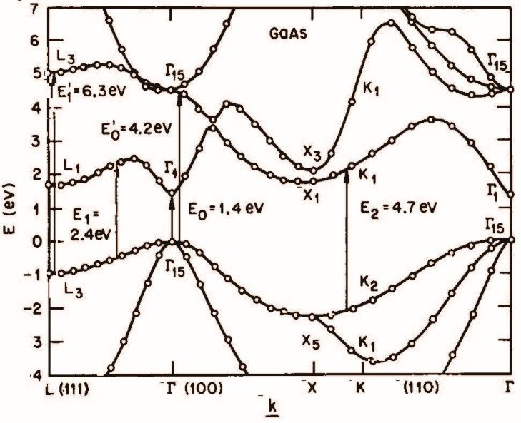
Quantum Condensed Matter Physics
        1. Classical and Semi-classical models for electrons in solids (3L)
        2. Electrons and phonons in periodic solids (6L)
        3. Experimental probes of band structure (4L)

        Photon absorption; transition rates, experimental arrangement for
        absorption spectroscopy, direct and indirect semiconductors, excitons.
        Quantum oscillations; de Haas-Van Alphen effect in copper and
        strontium ruthenate. Photoemission; angle resolved photoemission
        spectroscopy (ARPES) in GaAs and strontium ruthenate. Tunnelling;
        scanning tunnelling microscopy. Cyclotron resonance. Scattering in
        metals; Wiedemann-Franz law, theory of electrical and thermal
        transport, Matthiessen’s rule, emission and absorption of phonons.
        Experiments demonstrating electron-phonon and electron–electron
        scattering at low temperatures.

        4. Semiconductors and semiconductor devices (5L)
        5. Electronic instabilities (2L)
        6. Fermi Liquids (2L)
QCMP Lent/Easter 2019                                                         12.2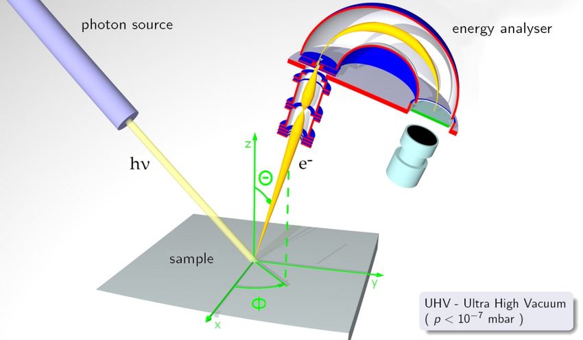
Photoemission

•   The most direct way to measure the electron spectral
    function is by photoemission
•   In a photoemission experiment photons are incident
    on a solid sample. Electrons are excited from
    occupied states in the band structure to states above
    the vacuum energy
•   The excited electron leaves the crystal and is
    collected in a detector that analyses both its energy
    and momentum
•   The incident photon carries very little momentum
    compared to the crystal momentum, so the
    momentum of the emitted electron parallel to the
    surface is close to that of its original state in the band
    structure of the solid
•   The perpendicular component of the momentum is
    not conserved – changes as electrons escape
    through surface                                              Density of states

QCMP Lent/Easter 2019                                                                12.3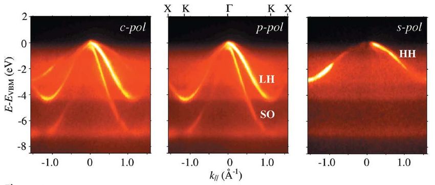
Photoemission
• We relate the energy of the outgoing electrons, E f , to the energy of the
incoming photons ω , the work function φ and the initial energy of the
electron in the solid Ei 2k 2
Ef = =Ei + ω − φ ,k f =ki
f
2m
• In this equation Ei is referenced to the Fermi energy EF , but E f is
referenced to the vacuum ground state energy
• We use the detector angle θ to find k with k = k f sin θ
• Problems occur if sample surface is rough as momentum parallel to the
surface is changed
• Photoemission data is easiest to interpret when there is little dispersion of
electron bands perpendicular to the surface – as in anisotropic layered
materials
• Analysing both the energy and momentum of the outgoing electron allows
the determination of the band structure directly. Integrating over all angles
gives a spectrum proportional to the total density of states.
• Photoemission gives information only about the occupied states – inverse
photoemission involves injecting an electron into a sample and measuring
the ejected photon, allowing the mapping of unoccupied bands
QCMP Lent/Easter 2019 12.4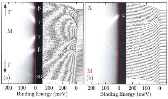
Angle Resolved Photoemission Spectroscopy (ARPES)
                         equipment

    wikipedia

•   ARPES Systems use ultrahigh
                                 −9
    vacuum techniques P ≤ 10 mbar so
    electrons travel to detector without
    encountering a gas atom
•   3-axis sample rotation
•   Cryogenic temperatures for samples
•   Detectors available for electron spin   Scientaomicron DA30 ARPES system
    direction measurements
QCMP Lent/Easter 2019                                                          12.5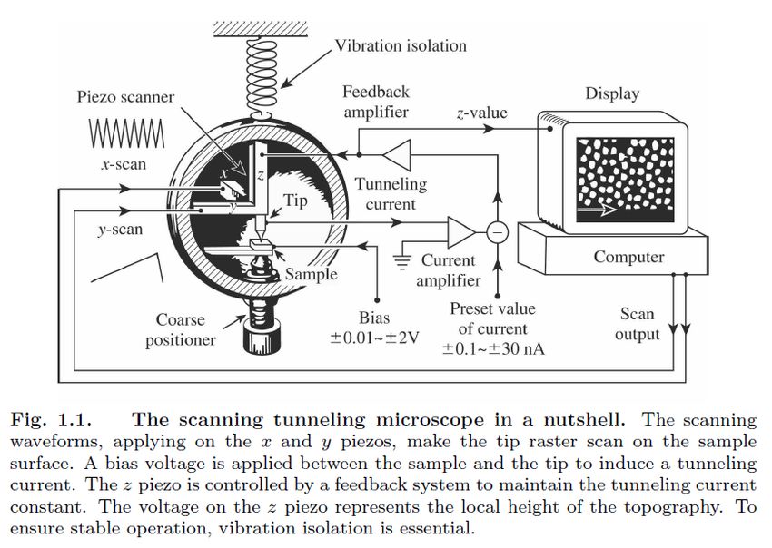
Angle resolved photoemission - GaAs                   GaAs
•    Sample is GaAs 50nm thin film doped with Be
     protected by 1nm thick As cap layer
•    Soft x-rays of different polarizations (893eV)
     give photo-electrons enough energy to escape.
•    ADRESS beamline at Swiss Light Source used
•    UHV conditions – 5x10-11mbar, T=11K
•    Thermal broadening 50-150meV
•    Results show Band dispersion E ( k ) including
     light hole, heavy hole and split-off hole bands
    M Kobayashi et al Appl Phys Lett 101, 242103 (2012)
    V N Strocov et al J Synch. Rad. 21, 32 (2014)

QCMP Lent/Easter 2019                                            12.6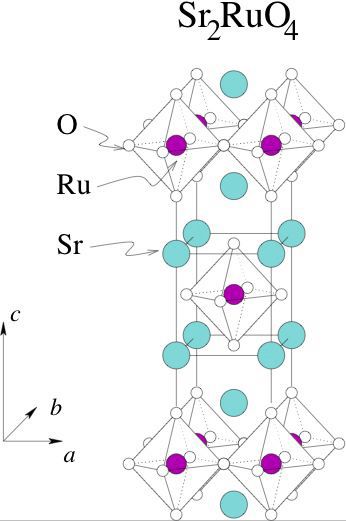
Angle resolved Photoemission - layered metal Sr2RuO4
•   28eV photons, electron energy
    resolution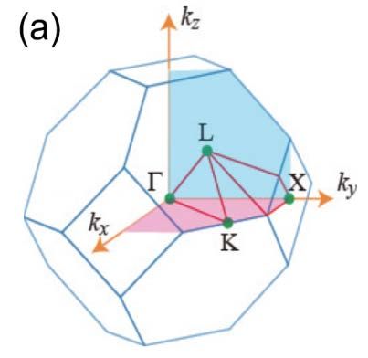
Tunnelling
•   Tunnelling spectroscopies, which inject or remove electrons through a
    barrier have now evolved to be very important probes of materials
•   A potential barrier allows a probe (usually a simple metal) to be maintained
    at an electrical bias different from the chemical potential of the material
•   The current passed through the barrier comes from non-equilibrium injection
    – tunnelling
•   Model for tunnelling from a metal into more complex material shown in figure
•   Current is given by integrated area
    between two chemical potentials –
    provided the matrix element for
    tunnelling is taken into account
•   If DoS for metal (or probe) – labelled 1      1
    is slowly varying, the differential          metal          2
    conductance dI / dV is proportional to                     sample
    DoS of material itself at the bias eV
    above the chemical potential µ 2

QCMP Lent/Easter 2019                                                         12.8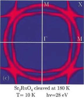
Tunnelling
• With the metal/probe (1) and sample (2) maintained at different electrical
potentials separated by a bias voltage, the current through the junction can
be predicted to be of the form µ
I∝
µ
∫
+ eV
g1 (ω )g 2 (ω )T (ω )dω
• Where T (ω ) is the transmission through the barrier for an electron of
energy ω and g1 , g 2 are the densities of states
• If the barrier is very high so T (ω ) is not a strong function of energy and if the
density of states in the contact/probe, g1, is approximately constant the
energy dependence comes from the density of states, g 2 inside the sample
being investigated
• Hence the differential conductivity is proportional to the density of states in
the sample
dI
∝ g 2 ( µ + eV )
dV
• It is difficult to maintain large biases so most experiments are limited to
probing electronic structure within a volt or so of the Fermi energy
QCMP Lent/Easter 2019 12.9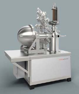
Scanning tunnelling microscopy
•   A scanning tunnelling microscope (STM) uses a sharp metal tip positioned
    by 3 piezoelectric transducers with vacuum as the tunnel barrier.
•   The tunnelling probability is an exponential function of the barrier thickness
•   High spatial resolution possible - 0.1nm lateral and 0.01nm depth, individual
    atoms can be imaged and manipulated despite nm or larger tip
•   Tip close to surface - electron
    wavefunctions overlap
•   On applying bias to sample a
    tunnel current is measured
•   Current converted to a
    voltage and fed back to the z-
    piezo controller to keep the
    current constant
•   Z piezo voltage gives surface
    topography when scanned
•   Invented by Binnig and Roher
    at IBM labs in Zurich - won
    Nobel prize in 1986                 Introduction to scanning tunnelling microscopy C J Chen
                                             G Binnig et al Appl Phys Lett 40, 178 (1982)
QCMP Lent/Easter 2019                        G Binnig et al Phys Rev Lett 49, 57 (1982)     12.10
Scanning tunnelling microscopy
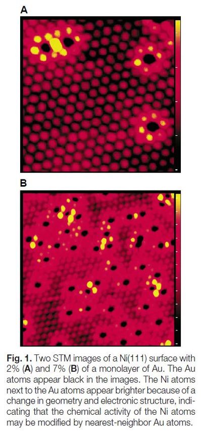
catalysts
• Scanning tunnelling microscopy used to study
processes on single crystal surfaces
• E.g. design of new catalysts - in this case to
produce hydrogen from hydrocarbons and water
• STM image shows the surface of a Ni single
crystal
• Some of the Ni atoms are substituted by Au
atoms. The Au atoms are darker and the Ni
atoms around a Au atom are brighter
• This is not because the Au atoms are
depressed but they have a lower local DoS and
the Ni atoms adjacent to a Au atom have
enhanced DoS due to perturbation by Au atom
• Because DoS is closely related to catalytic
reactivity the perturbed Ni atoms are more
highly reactive and act as a better catalyst
QCMP Lent/Easter 2019 F Besenbacher et al Science 279, 1913 (1998) 12.11Scanning tunnelling microscopy – positioning single atoms
• The tip is positioned above the
adatom to be moved
• The tunnelling current is increased
lowering the tip until the tip/adatom
interaction energy reaches diffusion
activation – where adatom can move
across ridge between stable positions
• Pull atom to desired location, reduce
current to move tip away
• In UHV at 4K Fe atoms can be moved
on Cu(111) surface to form a 48 atom
ring with a diameter of 7.13nm
• Atom ring acts to confine Cu surface
state electrons
• Tunnelling spectroscopy shows
discrete resonances in local density
of states indicating size quantisation
QCMP Lent/Easter 2019 M F Crommie et al Science 262, 291 (1993) 12.12Cyclotron resonance
• It is possible to make a direct measurement of the cyclotron resonance
frequency ωc = eB / m and hence effective mass using millimetre waves or
∗
far infrared radiation to excite transitions between Landau levels
• This experiment is known as cyclotron resonance
• For semiconductor samples which have much lower carrier density than
metals, the radiation can easily penetrate samples
• Measurements are usually made in
transmission, either by fixing the
magnetic field and varying the energy
of the radiation or using a fixed
frequency source such as a far infra-
red laser (shown here) and sweeping
the magnetic field detecting the
radiation with a bolometer.
• The linewidth of the resonance gives
information about the scattering rate
• In lightly doped samples carriers must be excited into bands by raising the
temperature or illuminating the samples with above bandgap radiation
QCMP Lent/Easter 2019 12.13Cyclotron resonance in Ge
• Figure shows absorption by cyclotron
resonance in a single crystal of Ge at
4K
• Electrons and holes present because
of above bandgap illumination
• Microwave frequency 24GHz and
magnetic field applied in (110) plane
at 60 degrees to [100] axis
• Resonance due to light and heavy
holes visible as are three electron
resonances
• The three electron resonances occur
because the anisotropic band minima
lie along [111] axes and the static
magnetic field makes three different
angles with these 4 axes
• Experimental and calculated effective
masses are shown in the figure
QCMP Lent/Easter 2019 G Dresselhaus et al Phys Rev 98, 368 (1955) 12.14Summary of Lecture 12 • Photoemission • Angle resolved photoemission spectroscopy (ARPES) • ARPES equipment • ARPES applied to GaAs and strontium ruthenate • Tunnelling, scanning tunnelling microscope (STM) • STM applied to catalysts and positioning atoms • Cyclotron resonance - example germanium QCMP Lent/Easter 2019 12.15
Quantum Condensed Matter Physics
                                 Lecture 12

                                     The End

QCMP Lent/Easter 2019   http://www.sp.phy.cam.ac.uk/drp2/home   12.16
You can also read