Quantum Nanoscience IBS Conference on - ABSTRACT BOOK - IBS Conference on Quantum ...
←
→
Page content transcription
If your browser does not render page correctly, please read the page content below
IBS Conference on
Quantum Nanoscience
September 25th - 27th, 2019

Lee SamBong Hall,
Ewha Womans University, Seoul

ABSTRACT BOOK

                                1
PROGRAM CONTENTS
2019 IBS Conference on Quantum Nanoscience
Day Day Day
1 2 3
Wednesday, September 25, 2019 Thursday, September 26, 2019 Friday, September 27, 2019
09:00-09:15 Participants Registration 09:00 - 09:15 Coffee break 09:00 - 09:15 Coffee break
09:15-09:30 Opening Remarks from Andreas Heinrich Session 3 Session 4
Theory Challenges in Quantum Nanoscience Quantum Surface Science at the Nanoscale
Session 1
General Introduction General Introduction
What is Quantum Nanoscience? 09:15-10:00 09:15-10:00
Daniel Loss Taeyoung Choi
General Introduction
09:30-10:00 10:00-10:30 Jelena Klinovaja 10:00-10:30 Harald Brune
Andreas Heinrich
10:00-10:30 William D. Oliver 10:30-11:00 Martin B. Plenio 10:30-10:45 Deungjang Choi
10:30-11:00 Yonuk Chong 11:00-11:15 Stanislav Avdoshenko 10:45-11:00 Saiful Islam
11:00-11:30 Andrew Dzurak 11:15-11:30 Hosung Seo 11:00-11:40 Fabio Donati
11:30-13:00 Lunch 11:30-13:00 Lunch 11:40-13:00 Lunch
Session 2 13:00-14:00 Poster Session (Daesan Gallery) Session 5
Quantum Sensing with Nanoscale Systems A Chemical Route to Quantum Nanoscience
General Introduction 14:00-14:30 Coffee Break
PROGRAM ••••••••••••••••••••••••••••••••••••••••••••••••••••••••••••••••••••••••••••••
02
13:00-13:45 General Introduction
Ania Jayich 13:00-13:45
Roberta Sessoli
14:30-15:30 Poster Session (Daesan Gallery)
13:45-14:15 Jörg Wrachtrup 13:45-14:05 Yujeong Bae
ORGANIZERS •••••••••••••••••••••••••••••••••••••••••••••••••••••••••••••••••••••••
04
QNS Dedication Ceremony
14:15-14:30 Sangyun Lee 14:05-14:25 Taner Esat
14:30-15:00 Coffee Break 16:00-16:15 Ewha President 14:25-15:00 Coffee Break
WELCOME ••••••••••••••••••••••••••••••••••••••••••••••••••••••••••••••••••••••••••••••••••
05
15:00-15:15 Jungbae Yoon 16:15-16:30 IBS Acting President 15:00-15:20 Mykola Telychko
DAY 1
15:15-15:30 Kyunghoon Jung 16:30-17:30 Don Eigler 15:20-15:40 Ruoning Li
SESSIONS 1-2 ••••••••••••••••••••••••••••••••••••••••••••••••••••••••••••••••••••••••••
07
15:30-16:00 Donghun Lee 17:30-18:00 Art Contest Awards 15:40-16:00 Danna Freedman
16:30-17:30 QNS Building Tour 16:00-16:30 Wolfgang Wernsdorfer DAY 2
18:30-22:00 Excursion
18:00-20:00 Official Dinner 16:30-17:00 Arzhang Ardavan SESSION 3 •••••••••••••••••••••••••••••••••••••••••••••••••••••••••••••••••••••••••••••••••
33
17:00-17:15 Poster Awards
DAY 3
17:15-17:30 Closing remarks from Andreas Heinrich
SESSIONS 4-5 ••••••••••••••••••••••••••••••••••••••••••••••••••••••••••••••••••••••••••
47
17:30-17:45 Group Photo
INFORMATION ••••••••••••••••••••••••••••••••••••••••••••••••••••••••••••••••••••••••
78
2
COMMITTEE MEMBERS

    Organizing Committee
                                                                                                          Welcome Message
                                                                                                     Bringing the quantum nanoscience
    International          Andreas Heinrich
                           IBS Center for Quantum Nanoscience, Seoul, Korea (chair)
                                                                                                            community together

                           Roberta Sessoli
                           University of Florence, Italy
                                                                                               Welcome to the first international conference on quantum
                           Daniel Loss                                                         nanoscience.
                           University of Basel, Switzerland

                           Lieven Vandersypen                                                  The organizers believe that it’s time that we bridge our
                           Delft University, The Netherlands                                   various specialties as an overarching community of
                                                                                               quantum nanoscience researchers. With the growth of the
                           Ania Jayich                                                         number of researchers, funding, and importance of the
                           University of California at Santa Barbara, USA
                                                                                               wide-ranging impact of quantum coherent functionality the
                           Andrea Morello                                                      timing to do this is now.
                           University of New South Wales, Australia
                                                                                               Our goal for this conference is to share as a field in order
                                                                                               for us to recognize the collaboration opportunities that can
                                                                                               span the comprehensive nature of quantum nanoscience.
                                                                                               Whether this is your first time to Korea or your tenth, we
                                                                                               hope you’ll enjoy the beauty of Seoul in the Fall by going
    Domestic               Michelle Randall                                                    with your colleagues for walks full of discussions or alight
                           IBS Center for Quantum Nanoscience, Seoul, Korea (chair)            in the many excellent cafes our city has to offer.

                           Andreas Heinrich
                           IBS Center for Quantum Nanoscience, Seoul, Korea
                                                                                               Thank you for joining this exciting first
                                                                                               conference on quantum nanoscience and
                           Jihee Min                                                           being an important member of this growing
                           IBS Center for Quantum Nanoscience, Seoul, Korea
                                                                                               community.

                           Young Kuk
                           Daegu Gyeongbuk Institute of Science & Technology                   Chair

                           Yonuk Chong                                                         Director,
                           Korea Research Institute of Science and Standards, Daejeon, Korea   IBS Center for Quantum Nanoscience,
                                                                                               Seoul, Korea
                           Donghun Lee
                           Korea University, Seoul, Korea

4                                                                                                                                                             5
IBS Conference on
    Quantum Nanoscience
    September 25th - 27th, 2019

    Lee SamBong Hall,                                  DAY
    Ewha Womans University, Seoul

                                    Wednesday, September 25, 2019

                                                SESSION 1

                                                SESSION 2

6                                                                   7
SESSION

              What is Quantum Nanoscience?

    Quantum nanoscience is the intersection of quantum
        science and nanoscience. In this session, we will
      describe a working definition as well as interesting
      concepts and examples of quantum systems at the
    nanoscale that enable quantum-coherent functionality.

                              Andreas Heinrich
          Director of IBS Center for Quantum Nanoscience, Seoul, South Korea
                                “What is Quantum Nanoscience?”

                              William D. Oliver
    MIT Department of Physics and Director at MIT Lincoln Laboratory, Boston, USA
               “Quantum Nanoscience and Engineering of Superconducting Qubits”

                                 Yonuk Chong
                 University of Science and Technology (UST), South Korea
             “Brief summary of the quantum computing strategic planning 2017-2018,
                     and quantum computing research program in Korea 2019”

                               Andrew Dzurak
       School of Electrical Engineering and Telecommunications, UNSW, Australia
    “Silicon-based quantum computing: The path from the laboratory to industrial manufacture”

8                                                                                               9
SESSION 1                                                                            WHAT IS QUANTUM NANOSCIENCE?     Notes

                                   What is Quantum Nanoscience?
                                                    Andreas Heinrich
              Center for Quantum Nanoscience, Institute for Basic Science (IBS), Seoul 03760, Republic of Korea.
                      Department of Physics, Ewha Womans University, Seoul 03760, Republic of Korea.
                                              *heinrich.andreas@qns.science

        Quantum mechanics was born out of the necessity to describe the physics of particles, atoms and
     molecules. At the scale of nanometers, the quantum uncertainty principle completely rules the static and
     dynamic properties of matter and fields. Does this mean that all of quantum physics is “nano”, and all of
     nanoscience is “quantum”? We suggest, provocatively, that the answer should be “no”. We propose instead
     an aspirational definition of Quantum Nanoscience: the search for quantum coherence-enhanced functionality
     at the nanoscale, see figure 1. This definition helps identify a field of research where quantum physics and
     nanoscience are not just a mutual necessity, but a mutual benefit.

         Quantum computing is a clear example where coherence-enhanced functionality is key to providing a
     radical departure from the mere operation of nanometer-scale devices. Semiconductors can host quantum
     information encoded in buried dopant atoms or quantum dots. Purely superconducting qubits, while
     physically much larger than the nanoscale, require accurate control over atomic-scale defects and nanometer-
     thin Josephson junctions. Bottom-up strategies for building quantum bits include chemically-synthesized
     magnetic molecules and atomic-scale devices built by scanning probes.

        Coherent quantum states are extremely sensitive to their environment. This can be exploited to design
     quantum-enhanced sensors, capable of detecting e.g. magnetic and electric fields, or temperature, with
     unprecedented sensitivity. Their nanometer size allows the sensing to occur at the scale of molecules or cells,
     of great interest for chemical or medical applications.

        We believe that the time is right to start an international conference on Quantum Nanoscience, since the
     interest in the community has strongly increased over the last decade and scientists now believe that there is
     great value in harnessing the quantum-coherent behavior of nanoscale systems.

                                            Figure 1. Q
                                                       uantum nanoscience strives for quantum-coherent functionality of
                                                      nanostructures.

10                                                                                                                                 11
SESSION 1                                                                                   WHAT IS QUANTUM NANOSCIENCE?          Notes

                               Quantum Nanoscience and Engineering
                                    of Superconducting Qubits
                                                        William D. Oliver
                       Department of Electrical Engineering and Computer Science, Department of Physics,
                               Research Laboratory of Electronics, and MIT Lincoln Laboratory
                                              Massachusetts Institute of Technology
                                                     Cambridge, MA 02139
                                                 *E-mail:william.oliver@mit.edu

        Superconducting qubits are coherent artificial atoms assembled from electrical circuit elements and
     microwave optical components[1]. Their lithographic scalability, compatibility with microwave control, and
     operability at nanosecond time scales all converge to make the superconducting qubit a highly attractive
     candidate for the constituent logical elements of a quantum information processor[2,3]. In this talk, we review
     the promise, progress, and challenges of engineering systems of superconducting qubits, with an emphasis on
     the important role quantum nanoscience will play in this endeavor[4,5].

     References
     [1] P. Krantz, M. Kjaergaard, F. Yan, T.P. Orlando, S. Gustavsson, W.D. Oliver, “A Quantum Engineer’s Guide to Supercon-
     ducting Qubits,” Appl. Phys. Reviews 6, 021318 (2019) | arXiv:1904.06560
     [2] M. Kjaergaard, M.E. Schwartz, J. Braumueller, P. Krantz, J.I-J. Wang, S. Gustavsson, W.D. Oliver, “Superconducting qu-
     bits: Current state of play,” arXiv:1905.13641
     [3] D. Rosenberg, D.K. Kim, R. Das, D. Yost, S. Gustavsson, D. Hover, P. Krantz, A. Melville, L. Racz, G.O. Samach, S.J. We-
     ber, F. Yan, J. Yoder, A.J. Kerman, W.D. Oliver, “3D integrated superconducting qubits,” npj Quantum Information 3, 42 (2017)
     | arXiv:1706.04116
     [4] W.D. Oliver and P.B. Welander, “Materials in Superconducting Qubits,” MRS Bulletin 38, 816-825 (2013)
     [5] J.I-J. Wang, D. Rodan-Legrain, L. Bretheau, D.L. Campbell, B. Kannan, D. Kim, M. Kjaergaard, P. Krantz, G.O. Samach, F.
     Yan, J.L. Yoder, K. Watanabe, T. Taniguchi, T. P. Orlando, S. Gustavsson, P. Jarillo-Herrero, W.D. Oliver, “Coherent control of
     a hybrid superconducting circuit made with graphene-based van der Waals heterostructures,” Nature Nanotechnology 14, 120-
     125 (2019) | arXiv:1809.05215

12                                                                                                                                             13
SESSION 1                                                                         WHAT IS QUANTUM NANOSCIENCE?     Notes

      Brief summary of the quantum computing strategic planning 2017-
       2018, and quantum computing research program in Korea 2019
                                                     Yonuk Chong
                      Korea Research Institute of Standards and Science (KRISS), Daejeon 34113, Korea
                            University of Science and Technology (UST), Daejeon 34113, Korea
                                                  *E-mail:yonuk@kriss.re.kr

        In this short talk, I will provide a brief summary of our (KRISS) past activities on the strategic planning
     of the quantum computing research in Korea. In 2017-2018, a team of scientists in KRISS tried to listen to
     the community’s diverse opinions about what is really relevant to quantum computing research, what we
     should do first, and how we may do it best, and then tried to summarize them to generate an open document
     which is readable by general audience. The final document was neither satisfying nor complete, but anyway
     a short document was published in mid-2018. In addition, as a separate topic, I will briefly introduce the first
     quantum computing research program in Korea launched in 2019. Finally, for the scientific part, I will briefly
     introduce our own research group’s activity on superconducting quantum computing research which is on-
     going in KRISS.

        * All these presentation contents are purely the opinion of the KRISS scientists. None of this presentation
     represents, or related to, any government policies or activities.

14                                                                                                                              15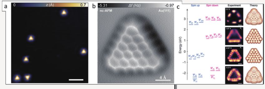
SESSION 1                                                                            WHAT IS QUANTUM NANOSCIENCE?       Notes

                         Silicon-based quantum computing:
                The path from the laboratory to industrial manufacture
                                                     Andrew Dzurak
                                                  UNSW – Sydney, Australia
                                                *E-mail: a.dzurak@unsw.edu.au

        In this talk I will give an overview of the development of silicon-based quantum computing (QC), from the
     basic science through to its prospects for industrial-scale commercialization based on CMOS manufacturing.
     I begin with Kane’s original proposal[1] for a silicon quantum computer, conceived at UNSW in 1998, based
     on single donor atoms in silicon, and will review the first demonstrations of such qubits, using both electron
     spins[2,3] and nuclear spins[4]. I then discuss the development of SiMOS quantum dot qubits, including the
     demonstration of single-electron occupancy[5], high-fidelity single-qubit gates[6], and the first demonstration
     of a two-qubit logic gate in silicon[7], together with the most recent assessments of silicon qubit fidelities[9,10].
     I will also explore the technical issues related to scaling a silicon-CMOS based quantum processor[8] up to the
     millions of qubits that will be required for fault-tolerant QC. Finally, I will discuss the broader effort in quantum
     information in Australia and a new company – Silicon Quantum Computing P/L – which was established last
     year to commercialize Australian research in this field.

     Acknowledgments
     We acknowledge support from the US Army Research Office (W911NF-17-1-0198), the Australian Research
     Council (CE11E0001017), and the NSW Node of the Australian National Fabrication Facility. The views and
     conclusions contained in this document are those of the author and should not be interpreted as representing the
     official policies, either expressed or implied, of the Army Research Office or the U.S. Government. The U.S.
     Government is authorized to reproduce and distribute reprints for Government purposes notwithstanding any
     copyright notation herein.

     References
     [1] B. E. Kane, Nature 393, 133 (1998).
     [2] A. Morello et al., Nature 467, 687 (2010).
     [3] J.J. Pla et al., Nature 489, 541 (2012).
     [4] J.J. Pla et al., Nature 496, 334 (2013).
     [5] C.H. Yang et al., Nature Communications 4, 2069 (2013).
     [6] M. Veldhorst et al., Nature Nanotechnology 9, 981 (2014).
     [7] M. Veldhorst et al., Nature 526, 410 (2015).
     [8] M. Veldhorst et al., Nature Communications 8, 1766 (2017).
     [9] H. Yang et al., Nature Electronics 2, 151 (2019).
     [10] W. Huang et al., arXiv.1805.05027, to appear in Nature, 13 May (2019).

16                                                                                                                                   17
SESSION
                Quantum Sensing with Nanoscale Systems

                Quantum systems can make incredibly sensitive sensors
                      of their environment. At the nanoscale this can be
                               combined with high spatial resolution.

                                                  Ania Jayich
                                            Department of Physics, UCSB, USA

                “Nitrogen-vacancy center spins in diamond for quantum technologies: progress and challenges”

                                              Jörg Wrachtrup
                                Physics Department of University of Stuttgart, Germany

                              “Analyzing chemical and structural composition by nanoscale NMR”

                                                     Sangyun Lee
            Physikalisches Institute and Research Center SCOPE and Integrated Quantum Science and
                               Technology (IQST), University of Stuttgart, Germany
      “Electrical charge state manipulation of single silicon vacancies in a silicon carbide quantum optoelectronic device”

                                                    Jungbae Yoon
                                                   Korea University, Korea
                     “Quantum Sensing Based on Diamond NV centers and its application for bio samples”

                                                  Kyunghoon Jung
     Department of Physics and Astronomy, and Institute of Applied Physics, Seoul National University, Korea
     “Deep Learning Approach for Efficient Spectral Decomposition of Spin Resonance to Detect Nuclear Spins in Diamond”

                                                 Donghun Lee
                                  Physics Department of Korea University, South Korea
                                “Sensing strain and magnetic field with quantum point defects”

18                                                                                                                            19
SESSION 2 QUANTUM SENSING WITH NANOSCALE SYSTEMS Notes
Nitrogen-vacancy center spins in diamond for quantum
technologies: progress and challenges
Dolev Bluvstein, Zhiran Zhang, Claire McLellan, Tim Eichhorn, Alec Jenkins, Simon Meynell,
Susanne Baumann, and Ania Bleszynski Jayich*
Department of Physics, University of California, Santa Barbara, CA 93106, USA
*E-mail: ania@physics.ucsb.edu
The nitrogen vacancy (NV) center defect in diamond is a powerful quantum-enabled technology, in
particular in the realm of sensing and imaging with ultra-high spatial resolution. In the first part of this talk, I
discuss recent experiments on NV-based, nanoscale imaging of condensed matter systems. The performance
of these solid-state quantum sensors is highly dependent on their quantum coherence and charge-state
stability, which are sensitive to their local environment. Surfaces are an important part of the defect’s
environment, in particular when targeting high spatial resolution sensing, which necessitates close proximity
between the sensor and target. To identify and mitigate the deleterious environmental effects, I discuss several
materials-based and quantum-control approaches. Specifically, I discuss the formation of highly-coherent NV
centers via a gentle, bottom-up method of nitrogen delta-doping during chemical vapor deposition growth of
diamond thin films followed by low energy (~ 150 keV) electron irradiation. I present measurements of the
density and coherence properties of the NV centers formed in this way as a function of growth and irradiation
parameters[1]. In the second part of the talk, I discuss the spin and charge state properties of shallow NV
centers, and introduce techniques to mitigate decoherence due to paramagnetic surface spins[2] as well as
charge state instabilities near surfaces[3]. These approaches to improved sensors will ultimately enable truly
nanoscale spatial resolution imaging of magnetic, electric, and thermal fields in a variety of condensed matter
and biological systems.
References
[1] “Optimizing the formation of depth-confined nitrogen vacancy center spin ensembles in diamond for quantum sensing”,
T. R. Eichhorn, C. A. McLellan, A. C. Bleszynski Jayich, https://arxiv.org/abs/1901.11519
[2] "Extending the Quantum Coherence of a Near-Surface Qubit by Coherently Driving the Paramagnetic Surface
Environment", Dolev Bluvstein, Zhiran Zhang, Claire A. McLellan, Nicolas R. Williams, Ania C. Bleszynski Jayich,
https://arxiv.org/abs/ 1905.06405
[3] "Identifying and mitigating charge instabilities in shallow diamond nitrogen-vacancy centers”, D. Bluvstein, Z. Zhang, A.
C. Bleszynski Jayich, Phys. Rev. Lett. 122, 076101 (2019)
20 21SESSION 2 QUANTUM SENSING WITH NANOSCALE SYSTEMS Notes
Analyzing chemical and structural composition by nanoscale NMR
Jörg Wrachtrup
3rd Institutes of Physics and Centre for Applied Quantum Technologies, University of Stuttgart, Stuttgart, Germany
*E-mail: j.wrachtrup@pi3.uni-stuttgart.de
Nuclear magnetic resonance (NMR) is one of the mostly used analytical techniques in material science,
biology and medicine. It provides unprecedented insight into structure and chemical composition. Yet, its
sensitivity is low and hence NMR has been restricted to measuring macroscopic sample volumes so far. With
the invent of nanoscale quantum sensing, however, NMR of a few and even single nuclear spins has become
feasible[1]. A long standing challenge has been to achieve high spectral resolution. By using quantum memories
or classical correlation methods, NMR on small sample volumes with sub-Hz spectral resolution has become
feasible, unleashing the full potential of NMR on the nanoscale[2]. The talk will describe recent progress utilizing
quantum algorithms to improve nanoscale NMR and show its use in measuring structures and dynamical
processes[3,4].
References
[1] T. Staudacher, F. Shi, S. Pezzagna et al. Science 339, 561 (2013)
[2] N. Aslam, M. Pfender et al. Science 357, 67 (2017)
[3] F. Shi, Q. Zhang et al. Science 347, 1135 (2015)
[4] T. Staudacher, N. Raatz, et al. Nature Com. 6, 8527 (2015)
22 23SESSION 2 QUANTUM SENSING WITH NANOSCALE SYSTEMS Notes
Electrical charge state manipulation of single silicon vacancies in a
silicon carbide quantum optoelectronic device
Matthias Widmann1*, Matthias Niethammer1, Dmitry Yu. Fedyanin2, Igor A. Khramtsov2,
Torsten Rendler1, Ian D. Booker3, Jawad Ul Hassan3, Naoya Morioka1, Roland Nagy1, Yu-Chen
Chen1, Ivan G. Ivanov3, Nguyen Tien Son3, Takeshi Ohshima4, Michel Bockstedte5,6,
Adam Gali7,8, Cristian Bonato9, Sang-Yun Lee1,10, and Jörg Wrachtrup1
1
Physikalisches Institute and Research Center SCOPE and Integrated Quantum Science and Technology (IQST), University of
Stuttgart, Pfaffenwaldring 57, 70569 Stuttgart, Germany
2
Laboratory of Nanooptics and Plasmonics, Moscow Institute of Physics and Technology, 9 Institutsky Lane, 141700
Dolgoprudny, Russian Federation
3
Department of Physics, Chemistry and Biology, Linköping University, SE-58183 Linköping, Sweden
4
National Institutes for Quantum and Radiological Science and Technology, Takasaki, Gunma 370-1292, Japan
5
Department Chemistry and Physics of Materials, University of Salzburg, Jakob-Haringer-Str. 2a, 5020 Salzburg, Austria
6
Solid State Theory, University of Erlangen-Nuremberg, Staudstr. 7B2, 91058 Erlangen, Germany
7
Wigner Research Centre for Physics, Hungarian Academy of Sciences, PO. Box 49, H-1525 Budapest, Hungary
8
Department of Atomic Physics, Budapest University of Technology and Economics, Budafoki út 8., H-1111 Budapest, Hungary
9
Institute of Photonics and Quantum Sciences, SUPA, Heriot-Watt University, Edinburgh EH14 4AS, UK
10
Center for Quantum Information, Korea Institute of Science and Technology, Seoul, 02792, Republic of Korea
Atomic-scale defects with stable fluorescence and long-lived spins are promising for quantum sensing and
quantum information. Such point defects can exist in different charge states, each of them with its distinct
optical and spin properties that can be possibly exploited for different applications. The charge state, however,
can fluctuate depending on the electronic environment and on the electromagnetic excitation used for control
and detection. Here, we investigate electrical charge state manipulation of individual silicon vacancies in silicon
carbide, one of the leading contenders for quantum technologies. We demonstrate how to manipulate the charge
state of single silicon vacancies in a silicon carbide p-i-n diode by applying a bias voltage. We also show that
control of electronic environment defined by the doping profile and distribution of other defects is a key for
charge state control at the nano-scale, which is evidenced by the enhanced photon emission rate under certain
conditions. Our findings open a way for deterministic control over the charge state of atomic-scale defects
in quantum devices and novel techniques for monitoring doping profile and voltage sensing in microscopic
devices.
24 25SESSION 2 QUANTUM SENSING WITH NANOSCALE SYSTEMS Notes
Quantum Sensing Based on Diamond NV centers and
its application for bio samples
Jungbae Yoon*, Kihwan Kim, Yuhan Lee, Myeongwon Lee, and Donghun Lee
Korea University
*E-mail: yjb4174@korea.ac.kr
There are increasing demands on highly sensitive magnetic field sensors both in fundamental research and
industrial fields. Diamond Nitrogen-Vacancy (NV) center is an atomic-scale quantum sensor that can meet
the demands as it provides high magnetic field sensitivity over wide bandwidth of detection frequency (e.g.
sensitivity < nT/Hz^1/2 and bandwidth DC ~ 1 GHz). It also provides nanometer scale spatial resolution
suitable for high resolution imaging applications and miniaturized sensing devices. Moreover, as NV center
even works at room temperature and is non-toxic, it is one of the powerful candidate of the nano-scale sensor
for the biological or medical application. We are building up a setup for widefield view image to acquire the
magnetic field distribution of magnetic samples such as magnetic nanowire. The setup and technique are
going to be adapted from solid state sample to the magnetic bio samples afterwards.
References
[1] M. Lee, et al., Nanotechnology 29, 405502 (2018)
26 27SESSION 2 QUANTUM SENSING WITH NANOSCALE SYSTEMS
Deep Learning Approach for Efficient Spectral Decomposition of Acknowledgement
The authors thank T.H. Taminiau for sharing their experimental CPMG data, which provides us with the way to
Spin Resonance to Detect Nuclear Spins in Diamond implement the cross-check regarding the performance of trained deep learning model.
Kyunghoon Jung*, Jiwon Yun, Kiho Kim, and Dohun Kim
Department of Physics and Astronomy, and Institute of Applied Physics, Seoul National University, Seoul 08826, Korea References
*E-mail: whitesands@snu.ac.kr [1] T. H. Taminiau, Detection and Control of Individual Nuclear Spins Using a Weakly Coupled Electron Spin, Phys. Rev. Lett.
109, 137602 (2012)
We present a novel machine learning approach to detect individual nuclear spins in diamond. Localizing [2] R. Santagati, Magnetic-Field Learning Using a Single Electronic Spin in Diamond with One-Photon Readout at Room
individual nuclear spins is the essential step to build coherently controllable spin resisters, which provides us Temperature, Phys. Rev. X 9, 021019 (2019)
with a robust base for quantum network, quantum simulation platform, or quantum memory. So far, to find these
nuclear spins, researchers have no alternative but to analyze spectrums manually so that there is no guarantee
to fully find those existent spins and to obtain accurate coupling parameters, especially due to the experimental
noise and its own complexity of signals.
Notes
Figure 1.
Figure 2. H
ere we introduce machine learning algorithm to automatically denoise and decompose the spectral data to
identify the location and to specify the characteristic of nuclear spins in diamond.
28 29SESSION 2 QUANTUM SENSING WITH NANOSCALE SYSTEMS Notes
Sensing strain and magnetic field with quantum point defects
Donghun Lee
Department of Physics, Korea University, Seoul, South Korea
*E-mail: donghun@korea.ac.kr
Various quantum systems have been studied in the field of quantum information, quantum network and
quantum metrology. Among the systems, atom-like point defect in diamond crystal has got great attention due
to its unique properties for quantum applications. Particularly nitrogen-vacancy (NV) centers in diamond are
solid-state spin-qubits possessing remarkable quantum properties applicable to various fields including quantum
information science and quantum sensing. For instance, its atomic-scale size, long spin coherence times, and
high field sensitivity are suitable for nanoscale magnetometry, electrometry, thermometry and so on.
In this talk, I will introduce current efforts and progress in our lab based on quantum point defects. Two
examples will be discussed; hybrid mechanical system for quantum information application and scanning probe
magnetometry for quantum sensing application. First, high-quality diamond mechanical oscillator is coupled to
embedded NV centers to realize hybrid quantum systems. Coherent mechanical control of NV’s spin and optical
properties will be demonstrated through strain associated with the resonator’s mechanical motion. Second, a
novel scanning probe microscope based on NV centers will be discussed. Combination of high spatial resolution
and high magnetic field sensitivity enables imaging of magnetic samples such as ferromagnetic nanowires and
Permalloy structures.
30 31IBS Conference on
Quantum Nanoscience
September 25th - 27th, 2019
Lee SamBong Hall, DAY
Ewha Womans University, Seoul
Thursday, September 26, 2019
SESSION 3
32 33SESSION
Theory Challenges in Quantum Nanoscience
Quantum Nanoscience has diverse needs for theoretical
investigations ranging from modelling with high precision to
the investigation and understanding of quantum coherence.
Daniel Loss
Department of Physics, University of Basel, Switzerland
“Ge and Si Nanowires: New Platforms for Spin and Majorana Qubits”
Jelena Klinovaja
Prof. Jelena Klinovaja Department of Physics, University of Basel, Switzerland
“Second Order Topological Superconductivity in π-Junction Rashba Layers”
Martin Plenio
Institute of Theoretical Physics in University of Ulm, Germany
“Quantum Control of Quantum Systems on the Nanoscale”
Stanislav Avdoshenko
Leibniz Institute for Solid State and Materials Research Dresden, Germany
“Theoretical study of Ho atom at MgO surface: valence electrons effect”
Hosung Seo
Department of Physics and Department of Energy Systems Research, Ajou University, Korea
“First-principles theory of single-photon emitters in two dimensional crystals for quantum information science”
34 35SESSION 3 THEORY CHALLENGES IN QUANTUM NANOSCIENCE Notes
Ge and Si Nanowires: New Platforms for Spin and Majorana Qubits
Daniel Loss
Dept. of Phys., Univ. of Basel, Switzerland
I will review recent theoretical results on holes in Ge and Si nanowires and their potential for quantum
computing platforms. The recent discovery[1] of an electrically induced spin-orbit interaction (SOI) of Rashba-
type in the low-energy hole states of Ge/Si (core/shell) nanowires provides an attractive scenario to realize
spin and topological qubits. Most remarkably, similar results apply to pure Si nanowires[2], which are fully
compatible with CMOS technology. Hole spins are particularly attractive since their p-wave orbitals have
minimal overlap with the nuclei resulting in long coherence times. Crucially the strong direct Rashba SOI
(DRSOI) is controlled by a moderate electric field applied perpendicular to the wire[1,2,3]. This enables the
electrostatic control of the coupling between the hole-spin degree of freedom and the electromagnetic field
along the wire. Exploiting this feature we have proposed a scalable surface code architecture obtained by
combining nanowire hole-spin qubits with a novel coplanar waveguide resonator grid structure[4]. Finally, the
DRSOI also opens up the door to create Majorana fermions in such Ge or Si nanowires when proximitized by
a superconductor[5].
References
[1] C. Kloeffel, M. Trif, and D. Loss, Phys. Rev. B 84, 195314 (2011).
[2] C. Kloeffel, M. J. Rancic, and D. Loss, Phys. Rev. B 97, 235422 (2018).
[3] C. Kloeffel, M. Trif, P. Stano, and D. Loss, Phys. Rev. B 88, 241405 (2013).
[4] S. Nigg, A. Fuhrer, and D. Loss, Phys. Rev. Lett. 118, 147701 (2017).
[5] F. Maier, J. Klinovaja, and D. Loss, Phys. Rev. B 90, 195421 (2014)
36 37SESSION 3 THEORY CHALLENGES IN QUANTUM NANOSCIENCE Notes
Second Order Topological Superconductivity in
π -Junction Rashba Layers
Jelena Klinovaja
Department of Physics, University of Basel, 4056 Basel, Switzerland
*E-mail: Jelena.klinovaja@unibas.ch
Recently, a lot of interest has been raised by the generalization of conventional TIs/TSCs to so-called
higher order TIs/TSCs. While a conventional d-dimensional TI/TSC exhibits (d − 1)-dimensional gapless
boundary modes, a d-dimensional n-th order TI/TSC hosts gapless modes at its (d − n)-dimensional
boundaries. In my talk, I will consider a Josephson junction bilayer consisting of two tunnel-coupled two-
dimensional electron gas layers with Rashba spin-orbit interaction, proximitized by a top and bottom s-wave
superconductor with phase difference ϕ close to π [1]. In the presence of a finite weak in-plane Zeeman field,
the bilayer can be driven into a second order topological superconducting phase, hosting two Majorana corner
states (MCSs). If ϕ=π, in a rectangular geometry, these zero-energy bound states are located at two opposite
corners determined by the direction of the Zeeman field. If the phase difference ϕ deviates from π by a critical
value, one of the two MCSs gets relocated to an adjacent corner. As the phase difference ϕ increases further,
the system becomes trivially gapped. The obtained MCSs are robust against static and magnetic disorder.
In the second part of my talk, I will switch from non-interacting systems [1,2], in which one neglects
effects of strong electron-electron interactions, to interacting systems and, thus, to exotic fractional phases.
I will show that this is indeed possible and explicitly construct a two-dimensional (2D) fractional second-
order TSC. I will consider a system of weakly coupled Rashba nanowires in the strong spin-orbit interaction
(SOI) regime. The nanowires are arranged into two tunnel-coupled layers proximitized by a top and bottom
superconductor such that the superconducting phase difference between them is π. In such a system, strong
electron-electron interactions can stabilize a helical topological superconducting phase hosting Kramers
partners of Z_2m parafermion edge modes, where m is an odd integer determined by the position of the
chemical potential. Furthermore, upon turning on a weak in-plane magnetic field, the system is driven into
a second-order topological superconducting phase hosting zero-energy Z_2m parafermion bound states
localized at two opposite corners of a rectangular sample.
References
[1] Y. Volpez, D. Loss, and J. Klinovaja, Phys. Rev. Lett. 122,126402 (2019).
[2] K. Plekhanov, M. Thakurathi, D. Loss, and J. Klinovaja, arXiv:1905.09241.
[3] K. Laubscher, D. Loss, and J. Klinovaja, arXiv:1905.00885.
38 39SESSION 3 THEORY CHALLENGES IN QUANTUM NANOSCIENCE
Quantum Control of Quantum Systems on the Nanoscale [8] J. Cai, B. Naydenov, R. Pfeiffer, L. McGuinness, K.D. Jahnke, F. Jelezko, M.B. Plenio and A. Retzker. Robust dynamical de-
coupling with concatenated continuous driving. New J. Phys. 14, 113023 (2012)
Martin B Plenio [9] Q.-Y. Cao, Z.-J. Shu, P.-C. Yang, M. Yu, M.-S. Gong, J.-Y. He, R.-F. Hu, A. Retzker, M.B. Plenio, C. Müller, N. Tomek, B.
Institute of Theoretical Physics and Center for Quantum BioSciences, Ulm University, Naydenov, L.P. McGuinness, F. Jelezko, and J.-M. Cai. Protecting quantum spin coherence of nanodiamonds in living cells.
Albert-Einstein Allee 11, 89081 Ulm, Germany E-print arXiv:1710.10744
*E-mail: martin.plenio@uni-ulm.de [10] J. Casanova, Z.-Y. Wang, I. Schwartz, and M.B. Plenio. Shaped Pulses for Energy-Efficient High-Field NMR at the nanosca-
le. Phys. Rev. Appl. 10, 044072 (2018)
Modern developments in quantum technologies are exploring a wide range of solid state based systems [11] J. Casanova, E. Torrontegui, M.B. Plenio, J.J. Garcia-Ripoll, and E. Solano. Modulated Continuous Wave Control for Ener-
as qubits for a wide variety of purposes of applications. Unlike atomic physics systems, which are operated gy-efficient Electron-nuclear Spin Coupling. Phys. Rev. Lett. 122, 010407 (2019)
under extreme conditions to ensure isolation from their environment, solid state based systems are by their
very nature in direct contact with the environment that is constituted by uncontrolled phonon, spin and charge
degrees of freedom that form part of the host material. As a result solid state qubits suffer significantly from
environmental noise. In order to address this challenge a combination of material science to improve the
hardware properties and of quantum control methods to further decouple the solid state qubits from their
environment while maintaining desired interactions are needed to achieve the ultimate goal of practically
usable coherent quantum dynamics. Notes
In this lecture I will present potential architectures for quantum simulation based on nuclear and electron
spins on diamond[1] and discuss how we can address the control issues that arise in such devices by means
of quantum control techniques. Questions such as enhanced resolution and addressing of single spins[2], high
fidelity quantum gates[3,4] and cooling, i.e. polarization, of spin ensembles[5,6,7] will be considered. Methods
to enhance the robustness of control procedures to control errors[8,9] as well as energy efficient control
schemes[10,11] will be discussed. While much of the discussion is motivated by the aim to control NV centers
in diamond, the concepts and protocols describe here are equally applicable to a wide variety of solid state
qubits.
References
[1] J.M. Cai, A. Retzker, F. Jelezko and M.B. Plenio. A large-scale quantum simulator on a diamond surface at room temperature.
Nature Physics 9, 168 -173 (2013)
[2] J. Casanova, J.F. Haase, Z.-Y. Wang and M.B. Plenio. Robust Dynamical Decoupling Sequences for Individual Spin Addres-
sing. Phys. Rev. A 92, 042304 (2015)
[3] J. Casanova, Z.-Y. Wang, and M.B. Plenio. Noise-resilient Quantum Computing with a Nitrogen-Vacancy Center and Nuclear
Spins. Phys. Rev. Lett. 117, 130502 (2016)
[4] Q. Chen, I. Schwarz, and M.B. Plenio. Dissipatively Stabilized Quantum Sensor Based on Indirect Nuclear-Nuclear Interac-
tions. Phys. Rev. Lett. 119, 010801 (2017)
[5] P. London, J. Scheuer, J.M. Cai, I. Schwarz, A. Retzker, M.B. Plenio, M. Katagiri, T. Teraji, S. Koizumi, J. Isoya, R. Fischer,
L.P. McGuinness, B. Naydenov and F. Jelezko. Detecting and polarizing nuclear spins with nuclear double resonance on a single
electron spin. Phys. Rev. Lett. 111, 067601 (2013)
[6] P. Fernández-Acebal, O. Rosolio, J. Scheuer, C. Müller, S. Müller, S. Schmitt, L.P. McGuinness, I. Schwarz, Q. Chen, A.
Retzker, B. Naydenov, F. Jelezko and M.B. Plenio. Towards hyperpolarisation of oil molecules via nitrogen-vacancy centers in
diamond. Nano Lett. 18, 1882 (2018)
[7] I. Schwartz, J. Scheuer, B. Tratzmiller, S. Müller, Q. Chen, I. Dhand, Z.-Y. Wang, Ch. Müller, B. Naydenov, F. Jelezko, and M.B.
Plenio. Robust optical polarization of nuclear spin baths using Hamiltonian engineering of nitrogen-vacancy center quantum dy-
namics. Sci. Adv. 4, eaat8978 (2018)
40 41SESSION 3 THEORY CHALLENGES IN QUANTUM NANOSCIENCE Notes
Theoretical study of Ho atom at MgO surface: valence electrons effect
Vasilij Dubrovin, Alexey A. Popov, and Stanislav M. Avdoshenko*
Leibniz Institute for Solid State and Materials Research Dresden, 01069 Dresden, Germany
*E-mail: s.avdoshenko@gmail.com
Detailed electronic structure of single atomic magnets is the most crucial bit in the further understanding
and design of a new generation of monatomic functional elements on surfaces and in another structural
setting. Recently, the inspirational single atomic experiment with Ho on MgO surfaces brought into a new
light a possibility to control and manipulate the quantum states of an atom[1,2]. However, these convincing
experiments are puzzling by the insufficient theoretical description. In this contribution, we looked at the
exact ab initio model for the Ho atom at MgO surface under a various level of complexity in an attempt
to resolve an experimental dilemma in the reported data. The research is based on the idea of the imminent
need to implement the local d - and p -shell electrons of Ho atom into the active space for proper system
consideration. By doing so, we have obtained the solution which complements experimental observations
without any additional assumptions.
Figure 1. A
rtistic representation of a single
ion EPR experiment involving a
single Ho atom placed on MgO
surfaces in the close proximity to
Fe (sensor). Ho moment is shown
as normal towards the MgO with
transparent “skirt” of the dipolar
field around it.
References
[1] F. Donati, et al., Science, 352, 318–321, 2016.
[2] F. D. Natterer, et al., Nature, 543, 226–228, 2017.
42 43SESSION 3 THEORY CHALLENGES IN QUANTUM NANOSCIENCE Notes
First-principles theory of single-photon emitters in two dimensional
crystals for quantum information science
Hosung Seo
Department of Physics and Department of Energy Systems Research, Ajou University, Suwon 16499, Republic of Korea
*E-mail: hseo2017@ajou.ac.kr
Deep-level spin defects in wide-gap semiconductors are promising platforms for applications in quantum
information processing, quantum sensing, and quantum photonics[1]. In particular, several point defects in
two-dimensional materials such as h-BN have recently emerged as room-temperature single photon emitters
(SPEs) with excellent optical stability and brightness[2] and potentially spin qubits[3]. In this study, we use
first-principles theory to investigate the optical and spin properties of deep-level defects in two-dimensional
crystals including h-BN and MoS2. First, we discuss our recent combined experimental and theoretical
study of Stark tuning of SPE’s in h-BN[4,5]. We show that it is possible to control the SPEs’ optical energy by
applying an out-of-plane electric field and we suggested that the presence of the out-of-plane dipole of the
SPEs may be originated from spontaneous symmetry breaking of the SPEs’ defect structure[4]. We consider
diverse defect candidates for SPEs in h-BN such as VNCB , VNNB and we discuss the potential mechanism
of the symmetry lowering process of the defect models and its physical implications for their application as
single photon emitters[5]. In the second part of the talk, we describe spin decoherence in two-dimensional
materials, using spin Hamiltonian and a cluster expansion method[6]. We show that isotopic purification
could be much more effective in 2D than in 3D materials. We also discuss additional factors influencing the
optimization of spin qubit hosts.
References
[1] W. F. Koehl, H. Seo, G. Galli, and D. A. Awschalom, MRS Bulletin 40, 1146-1153 (2015).
[2] M. Toth and I. Aharonovich, Annu. Rev. Phys. Chem. 70, 123 (2019)
[3] A. L. Exarhos, D. A. Hopper, R. N. Patel, M. W. Doherty, and L. C. Bassett, Nat. Comm. 10, 222 (2019).
[4] G. Noh, D. Choi, J. Kim, D. Im, Y. Kim, H. Seo, and J. Lee, Nano Lett. 18, 4710 (2018).
[5] J. Bhang, D. Yim, and H. Seo, in preparation (2019).
[6] M. Ye, H. Seo, and G. Galli, npj Comp. Mater. 5 , 44 (2019).
44 45IBS Conference on
Quantum Nanoscience
September 25th - 27th, 2019
Lee SamBong Hall, DAY
Ewha Womans University, Seoul
Friday, September 27, 2019
SESSION 4
SESSION 5SESSION
Quantum Surface Science at the Nanoscale
Surfaces of materials offer the opportunity to use scanning
probe techniques to measure their properties. This can be
combined with atomic-scale manipulation to build structures
with atomic-scale precision. Recently it has become possible to
perform quantum-coherent manipulation of atoms on surfaces.
Taeyoung Choi
IBS Center for Quantum Nanoscience and Department of Physics at Ewha, Seoul, South Korea
“Quantum surface science at Nanoscale"
Harald Brune
Institute of Physics, Ecole Polytechnique de Lausanne (EPFL), Lausanne
“Hyperfine Interactions and Intra-atomic Spin Excitations in Single Atom Magnets”
Deungjang Choi
Centro de Física de Materiales (MPC) CSIC-EHU, San Sebastián, Spain
“Cooper pair tunneling through a molecular junction”
Saiful Islam
Department of Chemistry, Graduate School of Science, Tohoku University, Japan
“Scanning tunneling Microscopy study of Electronic and Spin states of Single molecule magnet”
Fabio Donati
Center for Quantum Nanoscience and Department of Physics at Ewha, Seoul, South Korea
“Probing the magnetism of single atoms with orbital sensitivity"
48 49SESSION 4 THEORY CHALLENGES IN QUANTUM NANOSCIENCE Notes
Quantum surface science at Nanoscale
Taeyoung Choi and Andreas Heinrich*
Center for Quantum Nanoscience, Institute for Basic Science (IBS), Seoul 03760, Republic of Korea
Department of Physics, Ewha Womans University, Seoul 03760, Republic of Korea
*E-mail:choi.taeyoung@qns.science, heinrich.andreas@qns.science
Quantum nanoscience is an integrated and emerging field covering quantum physics and nanoscience. In
recent years, there have been significant advances to coherently control quantum properties of matter[1] and to
understand the properties of individual atoms, molecules, and their assemblies[2,3]. In particular, the center for
Quantum nanoscience (QNS) mainly focuses on the researches of nanoscale quantum systems in a solid-state
environment. . The first part of this talk introduces the overview of our research center and efforts - electron
spin resonance (ESR) on individual atoms and molecules[4,5], Nitrogen-Vacancy (NV) center in diamond[6],
and X-ray magnetic circular dichroism on atomic ensembles[7,8].
Secondly, we focus on our recent results about newly developed tool – ESR-STM. Here, we successfully
reproduce single-atom ESR on individual Fe atoms adsorbed on magnesium oxide (MgO). Utilizing a
2D vector magnetic field and the local field of the magnetic STM tip, we optimize the ESR signal and
characterize the role of the tip field. We demonstrate single atom ESR using only the tip-field, under zero
external magnetic field, which promises to make this technique available in many existing STM systems[5].
In the summary, QNS will explore the various quantum platforms and utilize them at surfaces as quantum
sensors, which possess superior spatial and energy sensitivity and possibly towards quantum bits, which
might enable quantum information processing at surfaces.
References
[1] T.D. Ladd, F. Jelezko, R. Laflamme, Y. Nakamura, C. Monroe, and J.L. O’Brien, Nature 464, 45 (2010)
[2] S. Loth, S. Baumann, C.P. Lutz, D.M. Eigler, and A.J. Heinrich, Science 335, 196 (2012)
[3] A.A. Khajetoorians, B. Baxevanis, Chr. Hübner, T. Schlenk, S. Krause, T.O. Wehling, S. Lounis, A. Lichtenstein, D.
Pfannkuche, J. Wiebe, and R. Wiesendanger, Science 339, 55 (2013)
[4] S. Baumann, W. Paul, T. Choi, C.P. Lutz, A. Ardavan, and A.J. Heinrich, Science 350, 417 (2015)
[5] P. Willke#, A. Singha#, X. Zhang#, T. Esat, A.J. Heinrich, and T. Choi, submitted
[6] J. Yoon, K. Kim, M. Lee, M. Choi, D. Kim, S. Kim, A.J. Heinrich, T. Choi, and D. Lee, in preparation.
[7] F. Donati, S. Rusponi, S. Stepanow, C. Wäckerlin, A. Singha, L. Persichetti, R. Baltic, K. Diller, F. Patthey, E. Fernandes, J.
Dreiser, Ž. Šljivančanin, K. Kummer, C. Nistor, P. Gambardella, and H. Brune, Science 315, 319 (2016).
[8] A. Singha, D. Sostina, C. Wolf, S. L. Ahmed, D. Krylov, A. Barla, S. Agrestini, P. Gargiani, M. Pivetta, S. Rusponi, H. Brune, A.
J. Heinrich, F. Donati, in preparation.
50 51SESSION 4 THEORY CHALLENGES IN QUANTUM NANOSCIENCE
Hyperfine Interactions and Intra-atomic Spin Excitations in Single References
[1] F. Donati et al, Science 352, 318 (2016).
Atom Magnets [2] F. D. Natterer et al. Nature 543, 226 (2017).
[3] F. D. Natterer et al. Phys. Rev. Lett. 121, 027201 (2018).
Harald Brune
[4] P. R. Forrester et al. Rev. Sci. Instrum. 89, 123706 (2018).
Institute of Physics, Ecole Polytechnique de Lausanne (EPFL), Station 3, CH-1015 Lausanne
[5] P. R. Forrester et al. submitted, see arXiv:1903.00242 for early version of this manuscript.
*E-mail: harald.brune@epfl.ch
[6] R. Baltic et al. Nanolett. 16, 7610-7615 (2016).
The magnetic states of single surface adsorbed atoms continue to surprise us and challenge our [7] M. Pivetta et al. Phys. Rev. B 98, 115417 (2018).
understanding. This includes the interaction of our observation tools with the systems of interest. Very few of [8] H. S. Li et al. J. Phys.: Condens. Matter 3, 7277 (1991).
the investigated systems bear potential for applications in magnetic information storage or as single magnetic [9] S. Rusponi et al. to be published.
quantum bits. We begin to understand what makes their magnetic states stable and why other systems are
paramagnetic.
Single Ho atoms on MgO(100)/Ag(100) are the smallest and most stable magnets known today[1-3]. At 8 T
external field, their onset temperature for switching from the metastable to the stable state is 45 K, and up to Notes
35 K their coercitive field is far above 8 T[3]. Their magnetic state can be read and written with tunnel electrons
[2]
. However, their ground state and zero-field stability remained open issues. Using anti-ferromagnetic tips
with robust zero-field spin-contrast[4], we determine the ground state and find that the nuclear spin states
convert avoided level crossings to real ones at zero field, while at small fields they create a series of avoided
level crossings. Landau-Zener tunneling at these crossings can be used to prepare the magnetic states without
implying electrons[5].
The second single-atom magnet published is Dy adsorbed on graphene/Ir(111)[6]. This system exhibits
spin-contrast of up to 60 pm apparent height difference between up and down magnetization. We interpret
this exceptionally large tunnel magneto resistance as 5d and 6s states being strongly polarized, due to Dy
transferring almost an entire electron to graphene[7].
Together with Dy, many other rare-earth atoms adsorbed on graphene exhibit intense high energy inelastic
conductance steps, see Figure to the right. Their origin is an intra-atomic spin-excitation between the 4f and
5d/6 spin-moments. For a given valence, the exchange energy between these moments is largely independent
of the 4f element[8]. Consequently, we observe a linear behavior of excitation energy with filling of 4f levels[9].
We finally show a few systems that “don’t work”, i.e., don’t show magnetic bi-stability, and explain why.
Figure 1.
52 53SESSION 4 THEORY CHALLENGES IN QUANTUM NANOSCIENCE Notes
Cooper pair tunneling through a molecular junction
Cristina Mier1, José Reina1, Leonard Garnier2, Benjamin Verlhac2, Laurent Limot2,
Nicolás Lorente1, and Deung-Jang Choi
1
Centro de Física de Materiales (MPC) CSIC-EHU, San Sebastián, Spain
2
Université de Strasbourg, CNRS, IPCMS, UMR 7504, Strasbourg, France
*E-mail: djchoi@dipc.org
The Josephson effect is the tunneling of Cooper pairs between two superconductors connected through a
weak link. The tunneling takes places through Andreev bound states (ABS) localized to the weak link. The
dependence of the ABS on the phase difference between the two superconductors fixes the way the Cooper
pairs tunnel. ABS are a characteristic of the junction and they cannot be probed by varying the bias between
the two superconductors since they take place at zero bias. This is very different from Yu-Shiba-Rusinov (YSR)
in-gap state that can take place already for one superconductor and are due to the weakening of Cooper pairs
produced by a magnetic impurity[1,2]. We will present experimental data and theoretical analysis characterizing
the ABS of a reproducible Scanning Tunneling Microscope molecular junction giving us access to the elusive
phase difference in an STM setup.
References
[1] Choi, D.-J. et al. Mapping the orbital structure of impurity bound states in a superconductor. Nat. Commun. 8, 15175 (2017).
[2] Choi, D.-J. et al. Influence of Magnetic Ordering between Cr Adatoms on the Yu-Shiba-Rusinov States of the β-Bi2Pd
superconductor, Phys. Rev. Lett., 120(16), 167001 (2018).
54 55SESSION 4 THEORY CHALLENGES IN QUANTUM NANOSCIENCE Notes
Scanning tunneling Microscopy study of Electronic and
Spin states of Single molecule magnet
Islam Saiful1, S.M.F. Shahed2, Tadahiro Komeda2, Keiichi Katoh1, and
Masahiro Yamashita1,3,4
Islam Saiful1, S.M.F. Shahed2, Tadahiro Komeda2, Keiichi Katoh1, and Masahiro Yamashita1,3,4,
1
Department of Chemistry, Graduate School of Science, Tohoku University, Japan
2
IMRAM, Tagen, Tohoku University, Japan
3
School of Materials Science and Engineering, Nankai University, Tianjin 300350, China
4
WPI Research Center, Advanced Institute for Materials Research, Tohoku University, 2-1-1 Katahira,
Aoba-Ku, Sendai 980-8577, Japan
*Email: saifulislamdu23@gmail.com
Single molecule magnets (SMM) represent a class of compounds in which a single molecule behaves as a
magnet. The reported blocking temperature, below which a single SMM molecule works as a quantum magnet,
has been increasing with the development in the molecular design and synthesis techniques of multiple-decker
Pc complex. Cerium intermetallics have raised a lot of interest for the past forty years thanks to their very
unusual and interesting electronic and magnetic properties. This can be explained by the peculiar electronic
configuration of Ce (4f 1) that allows different oxidation states leading to singular behavior such as quantum
phase transitions, heavy-fermion behavior and the Kondo effect. Scanning tunneling microscopy (STM) and
scanning tunneling spectroscopy (STS) have played an important role in the characterization of the molecule
film and its interface with the metal surface. In this work, we deposited double decker cerium phthalocyanine
molecule (CePc2) on Au (111) substrate. We clearly found eight lobes and Kondo resonance on center and
lobes. It forms two-dimensional lattice.
Figure 1. ( i) STM image of the double-decker CePc2 molecule (ii) dI/dV spectra position in a CePc2 molecule (iii) Cor-
responding dI/dV spectra
References
[1] Komeda, T. et al. Progress in surface science, 127 (2014)
56 57SESSION 4 THEORY CHALLENGES IN QUANTUM NANOSCIENCE Notes
Probing the magnetism of single atoms with orbital sensitivity
Fabio Donati
Center for Quantum Nanoscience, Institutes of Basic Science, Seoul 03760, Republic of Korea
Department of Physics, Ewha Womans University, Seoul 03760, Republic of Korea
*E-mail:donati.fabio@qns.science
Magnetic storage devices such as hard drives and magnetic tapes are massively used in conventional high-
capacity storage units. The increasing data-storage needs motivate the research towards novel fundamental
alternatives to achieve ever-larger bit density. Individual atoms adsorbed on a surface, with each atom being
able to store a single bit of data, could potentially allow maximal storage density in a solid-state system.
However, in order to store and process information, it is required to stabilize the electron spin of the magnetic
atoms against thermal and quantum fluctuations.
In the first part of this talk, I will present the rapid evolution of this field and the sequence of advancements
that led to the discovery of the first single atom magnet, namely a holmium atom on a magnesium oxide
ultra-thin film. Using x-ray magnetic circular dichroism (XMCD), we found these atoms to be magnetically
stable up to 40 K even in absence of an external magnetic field[1]. In addition, they can be read and written
individually using a scanning tunneling microscope[2,3].
In the second part, I will present the most recent advances towards the understanding of their magnetic
properties and the design of novel single atom magnets. We used XMCD to investigate the different
transitions accessible in the soft x-rays range to probe the spin magnetic moments with orbital sensitivity
and understand the magnetic level scheme of rare earth atoms on MgO/Ag(100). Finally, I will discuss the
strategies to realize novel single atom magnets with enhanced structural and magnetic stability, as well as the
first results obtained in this direction.
Figure 1. x -ray magnetic circular dichroism of single atoms with orbital sensitivity. Left: schematics of the soft-x-rays
absorption transitions. Right: XMCD signal of the M3 edge acquired on 0.10 ML (clusters) on 0.03 ML (atoms)
of Ho on MgO/Ag(100). Black lines show simulated transitions obtained from multiplet calculations.
References
[1] F. Donati et al., Science 352, 318 (2016).
[2] F. Natterer et al., Nature 543, 226 (2017).
[3] F. Natterer, F. Donati et al, Phys. Rev. Lett. 121, 027201 (2018).
58 59You can also read