ROADMAP: UK III-V COMMUNITY ENGAGEMENT WITH INDUSTRY - June 2012 1 - National Epitaxy ...
←
→
Page content transcription
If your browser does not render page correctly, please read the page content below
ROADMAP: UK III-V COMMUNITY
 ENGAGEMENT WITH INDUSTRY

          June 2012

              1
The production of this report was led by ESP KTN and resulted from a series of meetings
  and consultations organised by the EPSRC National Centre for III-V Technologies at the
request of EPSRC. Editing was undertaken by both organisations and publication is through
                                   the National Centre.

Document status Release 1, June 2012
Filename: III-V Roadmap_Release1(27.06.12).docx

                                           2
EXECUTIVE SUMMARY

III-V technologies have been key to many major lifestyle-influencing technologies such as the internet
(diode lasers), displays (light emitting diodes), optical data storage (lasers for DVD, Blu-ray), and mobile
phones (power amplifiers) and continue to play major roles in offering solutions to many of today’s societal
challenges. In addition, they provide highly novel structures and devices which reveal new fundamental
physical phenomena, leading to new device concepts and applications. The UK academic III-V community
has an extensive reputation for research excellence in this field. In addition there are a large number of
companies either engaged with the technology or able to offer exploitation routes where a strong market
pull is identified. Despite the importance of the sector and its significant potential for innovation, no
roadmapping exercise specific to potential impacts has previously been carried out. This report describes
the outcomes of a wide consultation across academia and industry, involving two workshops held in
Sheffield. It aims to inform strategic decision making in TSB and EPSRC, identify the important III-V
technologies to be developed and act as a reference to aid formation of new business activities,
collaborative clusters and academic proposal writing.

Within the confines of national priorities as articulated by the TSB and EPSRC, UK III-V capability and
capacity has been recorded and an evidence-based summary of the high impact technologies and the
required underpinning science identified. These application areas have all been identified as having a
strong market pull and their high potential for commercial exploitation is proof of the continuing vibrancy
of the sector. This exercise is seen as ongoing and this is expected to be ‘living’ document with future
update milestones identified.

Each of the outcome application areas and enabling technologies represent different degrees of
opportunity and potential for impact. However, future planning, such as value-chain analysis of each of
these areas is left to the formation of smaller groupings. For this to happen, clear pathways to funding
must be evident.

A major gap which is preventing rapid exploitation of concepts through to commercial realisation is the
lack of centralised infrastructure to produce the required device demonstrators. This gap has long been
recognised in many sectors and is being addressed by the establishment of ‘Catapult Centres’, but none so
far cover III-V technologies.

Recommendations to promote and support the sector are made: most important amongst these is the
establishment of a Knowledge Transfer (KT) Fellow for the III-V community, which we view as key to
keeping the momentum of this exercise going and to work across EPSRC, academia, TSB, and industry to
capitalise on a buoyant sector with strong UK capability.

CONTENTS

                                                     3
Executive summary ............................................................................................................................................ 3

1.1       Introduction ............................................................................................................................................ 6

1.2       Purpose and Scope.................................................................................................................................. 7

1.3       Target audience and impact ................................................................................................................... 7

1.4       Methodology........................................................................................................................................... 8

2.1       Application trends enabled by III-V semiconductors............................................................................ 11

2.2       Science trends enabled by III-V semiconductors .................................................................................. 12

2.3       III-V community impact on national and business priorities ................................................................ 14

2.4       UK Research and commercial supply chain .......................................................................................... 16

3.1       Application and technology matrix ....................................................................................................... 18

3.2       Medium term commercially-valuable opportunities ........................................................................... 20

   3.2.1        High data rate photonics for telecommunications and storage..................................... 20

   3.2.2        Medical equipment ....................................................................................................................... 23

   3.2.3        Gas sensing and monitoring equipment ....................................................................................... 25

   3.2.4        Terahertz imaging .......................................................................................................................... 27

   3.2.5        III-Vs used in manufacturing .......................................................................................................... 28

   3.2.6        UV Water purification.................................................................................................................... 30

   3.2.7        Efficient power electronics ............................................................................................................ 32

   3.2.8        New Photovoltaic materials .......................................................................................................... 34

   3.2.9        Hydrogen fuel generation.............................................................................................................. 36

3.3       Summary of III-V market opportunities ................................................................................................ 38

3.4       III-V academic-business gaps and opportunities .................................................................................. 40

3.5       Synthesis ............................................................................................................................................... 42

3.6       The roadmap ......................................................................................................................................... 43

3.7       Conclusions ........................................................................................................................................... 44

3.8       Recommendations ................................................................................................................................ 45

                                                                                 4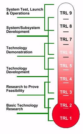
3.9       Acknowledgements............................................................................................................................... 46

3.10 Producers of the report ........................................................................................................................ 46

Annexes ............................................................................................................................................................ 47

   1      The questionnaire ................................................................................................................................. 47

   3      TRL detailed definitions ........................................................................................................................ 52

   4      Full listing of the roadmap .................................................................................................................... 53

                                                                                  5
SECTION 1: CONTEXT AND PURPOSE
1.1     INTRODUCTION

III-V technologies have an all-pervasive impact which has led to revolutionary innovations such as the
internet, wireless communications, mobile phones and optical data storage. The discipline provides the
basis for numerous newly-developed technologies, such as the injection laser, quantum cascade laser,
concentrator solar cells, mid infra-red detectors and modulation doped transistors (MODFETs) to name a
few, that impact many of the most important challenges faced by society. These have led to the foundation
of major industries on 10-15 year timescales. The UK has been a leader in many of the important
developments in III-Vs, and this builds on UK research excellence as measured in reports from EPSRC 1 and
BIS 2.

III-V research in UK universities is highly active in applied and fundamental fields. The long range research
with potential for major impact over the next 10 years is, as in the past, likely to be very fruitful. This
research has been made possible by significant and sustained investment over the last 30 years,
predominantly by EPSRC, in a number of institutions throughout the UK.

The provision of state-of-the-art equipment for the growth and characterisation of III-V crystals, and the
subsequent fabrication infrastructure needed to demonstrate fundamental effects as well as functional
devices, is absolutely crucial to maintaining these world class activities. EPSRC, in partnership with the TSB,
is committed to the support and promotion of the UK’s excellent research position to maximise the
economic and societal impact of their funded academic research and to help drive sustainable economic
growth over the long term1. As part of this policy, EPSRC encouraged the EPSRC National Centre for III-V
Technologies to take a leadership role in consulting the UK III-V community and producing a III-V
Semiconductors Roadmap with full engagement from both academia and industry. The diversity of
applications emanating from the work of the National Centre contributes significantly to providing impact
in the EPSRC priority areas of Manufacturing, Digital Economy, Energy and Healthcare technologies and the
similar TSB priority areas. With its strong connections to the wider UK III-V community, the National Centre
was well placed to fully engage with that community in carrying out the Roadmap exercise described in this
report. The ESP KTN provided valuable resources and experience for the exercise and production of this
document. Despite the strategic importance of III-Vs to the UK, as outlined above, no such roadmap had
been produced previously.

1
 Research Performance and Economic Impact Report 2010/2011, EPSRC, October 2011, Available at
http://www.epsrc.ac.uk/SiteCollectionDocuments/Publications/corporate/ResearchPerformanceAndEconomicImpactReport.pdf
Accessed 02.04.12
2
 Innovation and Research Strategy for Growth, Department for Business Innovation and Skills, December 2011 Available at
http://www.bis.gov.uk/assets/biscore/innovation/docs/i/11-1387-innovation-and-research-strategy-for-growth.pdf Accessed
02.04.12

                                                            6
1.2 PURPOSE AND SCOPE
Given the context above, this report attempts to assemble an evidence-based summary of the high impact
technologies and underpinning science in III-V Technologies, as related to significant national priorities or
commercial markets, with assessment of the whole UK III-V capacity and capability, both commercial and
academic. It is recognised that there are many important sectors not mentioned explicitly in this report
which are either allied to III-V technologies or which can directly benefit from them. An important outcome
from this exercise would be the identification of new, non-traditional collaborations across several sectors.
The authors canvassed the community and have collated a high level roadmap, which shows the consensus
opinion of the key technology themes, their likely outcomes in terms of product and services, and the
earliest impact these could make on both high-level market opportunities and on national priorities. This
was felt to be most appropriate and useful to the main stakeholders. The lessons drawn from recent
studies of the UK’s international competitors, and the existing UK innovation policy, are considered in
making the recommendations.
This document is structured in three sections:
• Section 1 The introduction , setting out the context, target audience and methodology
• Section 2 Current trends and UK positioning in terms of science, commerce or public policy
• Section 3 The key applications and technologies, the UK supply chain positioning, and possible
ways forward for the community, with opportunity/gap commentary and recommendations
This report does not encompass a detailed technology or market road-mapping activity, which would
require resources and time outside the scope and capability of the NC and ESP KTN; would require the
discovery of extensive commercially-sensitive material; and would require the authors to make many
assumptions which would be difficult to justify, and might lead to conflict with existing niche roadmaps.
1.3 TARGET AUDIENCE AND IMPACT
The main target audiences for this report are as follows, with some suggestions for the impact it may
make.
Audience Impact
The UK III-V community, including the Provide guidance for those routes to funding which address
National III-V Centre and those national priorities and maximise knowledge transfer.
supported by it.
The Research Councils, particularly Validation on impact of support to the III-V community, and
EPSRC, and other national funding input to future policy and strategy.
7bodies such as the TSB
Industry, and Research and Technology Provide an overview of the III-V community, and the key
organisations research directions, to inform engagement and possible
collaboration.
1.4 METHODOLOGY
The UK III-V community is highly diverse, varying from large commercial organisations with several points
of engagement in technology and markets, to SMEs providing niche capability. Moreover, since the
community makes a contribution in a variety of market and application sectors, they are networked in
different ways. For example, groups engage via attendance at the NC-run UK Semicon conferences,
through membership of groupings like the ESP KTN, through trade bodies like the UK Lighting Association
and Association of Laser Users (AILU) and through the normal academic community networks. As a result,
to date there has been no attempt to perform an overview survey of the III-V sector’s specific interests.
The closest recent coverage was probably through the TSB consultation, led by ESP KTN, on the case for a
Photonics-based Technology Innovation Centre 3
In order to consult as widely as practicable, and to capture the required information in a structured
roadmap, the NC engaged with the ESP KTN to support it with some best practice tools. The recommended
process and structure was informed by the report of the Cambridge University Institute for
Manufacturing4. A six-stage process was developed as below, culminating in a four-level roadmap with
complementary detailed notes:-
1. Early brainstorming by an expert group (from the NC Steering Committee) to identify the likely
boundaries of the sectors, both in terms of technology and application.
2. A workshop 5 was held in January 2011, largely for academic institutions but with strong industry
representation. Attendees numbered 101, composed of 73% academics and 27% industrialists.
The outputs included expert summary talks on each of EPSRC’s priority themes and a detailed
report on the extent of III-V academic engagement, industrial involvement, strengths and
weaknesses and exploitation opportunities.
3
Photonics Innovation Centre Consultation, ESP KTN (July 2011). Available at https://connect.innovateuk.org/web/photonics
Accessed 03.04.12
4
Roadmapping for Strategy and Innovation: aligning technology and markets in a dynamic world, Phaal R. et al, University of
Cambridge Institute for Manufacturing, (April 2010), Cambridge University Press.
5
First III-V Roadmapping Meeting, 13 January 2011, EPSRC III-V NC. Available at http://www.epsrciii-
vcentre.com/roadmapping%20exercise.aspx Accessed 28.02.12
83. A further, more industry-focussed workshop was held in May 2011, with the aim of identifying,
validating and prioritizing a list of III-V technologies and application sectors for future exploration.
Registrations numbered 77, composed of 60% academics and 40% industrialists. The outputs were
an “applications vs. technology matrix” covering the key applications sectors, prioritised by votes of
the participants.
4. Validation and extension of this summary through an email-based survey of about 400 UK
individuals with interests in III-V materials, devices, applications and processes. The questionnaire is
given at Annexe 1. A total of 34 additional responses were received. The results matrix is further
considered in Section 3.
5. Synthesis of all the above by ESP KTN into a summary report and pictorial roadmap with comment
on the key four features, namely
a. The underpinning actions by the community and the NC
b. Basic science and technology activities
c. The anticipated impacts for products and services
d. The earliest possible commercial or societal impact
This phase particularly makes use of ESP KTN market and technology intelligence and of existing
market and technology roadmaps like those of Photonics 21 and ITRS.
6. Review and adoption of the work and its conclusions by the NC and the wider III-V community, in
partnership with EPSRC.
The output roadmap is not to be seen as a static document, but more as a live resource which can be
updated by disparate users for their own purposes, and may need a formal update every few years in the
light of changes in technologies, applications, markets, or the supplier base. Moreover, given the very
nature of this road-mapping process, certain strengths and weaknesses of the UK’s position will become
apparent, so these are discussed briefly.
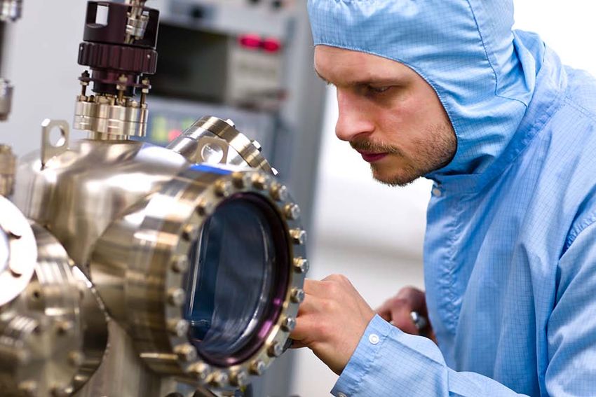
9Figure 1 The first workshop
10SECTION 2: CURRENT TRENDS AND UK
POSITIONING
2.1 APPLICATION TRENDS ENABLED BY III-V SEMICONDUCTORS
The widespread impact of III-V semiconductors arises from a combination of highly favourable
optoelectronic properties (which allow III-Vs to form the basis of lasers, LEDs and detectors, from the mm-
range to the ultraviolet), high carrier mobility and, crucially, the existence of highly advanced crystal
growth and device fabrication techniques. Epitaxial technologies (MBE and MOVPE) can produce multi-
layer nano-scale structures containing controlled compositions of materials within the III-V family, with
very high degrees of crystalline quality and interface perfection on an atomic scale. Such structures have
provided the basis for hugely important inventions which have led to the foundation of major industries
such as in optical communications, high frequency radar, LED lighting, satellite communications, mobile
telephones and optical detectors and imaging. The flexibility and width of capability of the materials
systems accessible by the III-V community is indicated in Figure 2, which shows some of the achieved
device types and their locations on a chart which summarises the available lattice constants and the
semiconductor energy gaps available.
11Visible and UV Light Power amplifiers for
Emitting Diodes, UV mobile phones Telecomms lasers
detectors
Photovoltaics
IR and terahertz emitters
(QCLs), detectors, IR imagers
GaN HFETs for RF
amplifiers and
power electronics High speed
electronics
Figure 2- Picture summarising the semiconductor energy gap vs the lattice constant of a few III-V semiconductor applications (modified from Laser Focus
World 6)
2.2 SCIENCE TRENDS ENABLED BY III-V SEMICONDUCTORS
The diversity of material properties within the III-V family, combined with the ability to control and
manipulate electronic and photonic properties via reduced dimensionality and nano-fabrication, provides
almost endless scope to study new areas of fundamental physics and to develop innovative approaches
towards new generations of devices with enhanced performance and functionality. Thus, while the field is
indisputably well-established, a multitude of opportunities remain for scientific discovery and technological
innovation. This is clearly evident from the numerous new areas that have emerged in recent years, such
as spintronics, dilute magnetic semiconductors, intersubband optoelectronics, coherent control of
quantum states, plasmonics, polaritonics, semiconductor metamaterials and III-V nanowires. Many of
these topics have been identified as key enabling technologies within the EU 7. The continuing
development of these and other emerging new areas, in addition to cross-disciplinary activities involving
the biological and medical sciences, ensures a vibrant, highly productive and innovative future for III-V
research for many years to come and these areas should determine future provision for UK research.
6
Photonics frontiers: 50 years of lasers: How laser output spread across the spectrum, Laser Focus World, (05.01.10). Available at
http://www.laserfocusworld.com/articles/print/volume-46/issue-5/features/photonic-frontiers.html Accessed 28.01.12
7
Information and communication technologies : Key Enabling Technologies , EU Commission (2009)
http://ec.europa.eu/enterprise/sectors/ict/key_technologies/index_en.htm Accessed 21.06.12
12III-V research in UK universities is highly active in applied and fundamental fields. Internationally
recognised areas include: quantum transport and tunnelling, ferromagnetic semiconductors, polariton and
quantum dot physics, short gate high speed FETs, external cavity surface emitting lasers, quantum dot and
quantum cascade lasers, micro-LEDs and wide band gap GaN-based devices. New materials such as, for
example, bismides, which have intrinsic properties offering performance improvements for lasers and
detectors are also important. Long range research with potential for major impact over the next 10 years
is likely to be equally fruitful, including control and coupling of single quantum states, quantum
information processing, spintronics, photonic band gap structures, Bose-Einstein condensation, wide band
gap materials, III-Vs on silicon and three dimensional growth of nanostructures. This research has been
made possible by significant and sustained investment over the last 30 years, predominantly by EPSRC, in a
number of institutions including the NC.
(Glasgow University)
132.3 III-V COMMUNITY IMPACT ON NATIONAL AND BUSINESS PRIORITIES
The wide impact of III-V semiconductors is demonstrated convincingly though consideration of Table 1,
which lists the TSB’s key priority themes and competences, which are potentially (blue) , or currently
(green)serviced by just a few III-V technology platforms.
Table 1 How the TSB priority themes are enabled by III-V semiconductor devices
TSB priority III-V technology platform
theme
III-V solar cells Wide band-gap III-V lasers III-V LEDs High-speed low- noise
electronic devices electronics
Energy Concentrator PV, High-temperature, and Efficient sources for Lower power
satellite power, H2 low-loss GaN transistor communications consumption, long-life
generation switches lighting
Built Distributed Reduced impact (smaller) Gas analysis for safety and “Wraparound”
Environment electricity base stations security. Distributed Fibre architectural displays
generation for Optic sensing for civil and lighting
Smart Grids engineering
Food Compact microwave Optical characterisation of UV sterilisation of liquids
sources for cooking “food decay”
Transport Battery top-up Efficient power High brightness , long- GaSb torque sensors
charging, H2 electronics for electric life headlights
generation vehicles
Healthcare Energy scavenging Photodynamic therapy, Blood oxygenation Pre-amplifiers for MRI
for wireless body breath diagnosis, surgery, monitors, Optical scanners, THz sources and
networks dermatology, cosmetics, Coherence Tomography detectors for cancer
dental decay imaging for ophthalmic and skin scanning
procedures, benign imaging, dental curing
prostatic hyperplasia
High Value Volume wafer Volume wafer processing Diode pumps for solid Volume wafer processing Volume wafer processing
Manufacturing processing and device and packaging state lasers and fibre and device and and device and packaging
lasers for material packaging
processing
Digital Remote power Energy efficient base Underpins optical Satellite, 3G and 4G
services supplies station electronics communications cellular phone networks, ,
infrastructure high speed optical
communications
14The TSB has implemented its policy in this sector through the Electronics, Sensors, Photonics (ESP)
strategy8 which highlights the SME-led and fragmented supply-chain, the high costs of development, and
picks out the following highly relevant themes and technology areas for focus:-
• Electronic Systems
• Photonics
• Sensor Systems
• Power Electronics
BIS identifies9 that government has a key role in
• Funding blue skies research as well as new discoveries and inventions - With specific BIS focus on,
among others, energy efficient computing, and Energy Harvesting
• Improving the interface between Higher Education Institutions (HEIs) and Business
• Delivering a better environment for commercialising research.
The Wilson Review 10 of relationships between academia and business provides several specific
recommendations, of which the most relevant are:
All full‐time postdoctoral research staff should have the
Recommendation 16,
opportunity to benefit from 8 to 12 weeks’ of work experience
paragraph 5.6:
outside academia every three years during their contract
Both business and university leaders should reflect upon their
Reflective recommendation 1,
organisational knowledge of the full landscape of business –
paragraph 3.3
university collaboration, and on the management of the
partnerships that they have. For universities this reflection should
extend to strategic decisions concerning the domains that the
university wishes to provide; for business it should extend to
matching needs to those universities that best meet their
requirements within the appropriate domain
8
Electronics, Sensors, Photonics strategy is included in the TSB’s Strategy for Technology 2012 -2015 document available at
http://www.innovateuk.org/publications/strategy-documents.ashx from July 2012
9
Innovation and Research Strategy for Growth , BIS, (Dec 2011), Available at
http://www.bis.gov.uk/assets/biscore/innovation/docs/i/11-1387-innovation-and-research-strategy-for-growth.pdf Accessed
28.02.12
10
Wilson, T, A Review of Business–University Collaboration, (Feb 2012) Available at http://www.wilsonreview.co.uk/wilson-
review/wilson-review.pdf Accessed 23.03.12
15Collaboration between universities in supplying business needs
Reflective recommendation 2,
can only benefit the university sector as a whole.
paragraph 3.4
Universities that work with employers through industry advisory
Reflective recommendation 10,
groups should consider including the existence of such a group, its
paragraph 4.6.1
membership and its influence, within the university’s enterprise
strategy and within the material that it provides to applicants and
students.
The activities and success of the UK academic III-V community in meeting these objectives and
recommendations is also a valid consideration in this roadmap.
2.4 UK RESEARCH AND COMMERCIAL SUPPLY CHAIN
In Table 2 we have presented a partial list of those companies and academic groups which have a
significant position in specific technology sectors.
Table 2 UK R&D and commercial supply-chain membership by technology platform (partial list, based on output from the 2nd workshop)
Technology Industry/academic capability or interest
Cambridge, RFMD (GaN on Si), IQE, Plessey Semicond, NXP, IR, e2v, Glasgow,
III-V epitaxy on Si Sheffield, UCL ,Warwick (SiGe), Bath (nanorods)
GaN DUV LEDs, lasers Cambridge, Bath, Sheffield
IQE, CST, CIP/Huawei, M2 lasers, Teraview, Cambridge, Leeds, Glasgow, Essex, UCL,
THz sources QMC, Cardiff, Manchester, Smiths Detection, e2v, St. Andrews.
Crystalline InGaN Cambridge, Sheffield, Nottingham
VCSELS Sheffield, Strathclyde
High To, high efficiency CIP/Huawei,CST, Oclaro, Cambridge, Cardiff, Surrey, Southampton, Sheffield, Gooch
lasers (QD) and Housego, Nottingham
GaN UV detectors Glasgow, Cambridge, Sheffield, Nottingham, IQE
16GaN HFETs/ switches Glasgow, Cambridge, Sheffield, Nottingham, IQE, IR, Plessey Semiconductors, NXP
InGaAs, InSb/AlInS, InAs
transistors Glasgow, Sheffield, Manchester
High speed optical
modulators CIP/Huawei, CST, Oclaro, Cambridge, Cardiff, Surrey, Southampton, Sheffield
Manchester, Sheffield, Glasgow, CIP/Huawei, Lancaster, Strathclyde, Warwick,
Oclaro, M2 lasers, CST, QMC, Cardiff, Optocap, Manchester, Teraview, Leeds, IQE ,
IR sources (including QCLs) Cambridge, UCL
Monolithic or hybridised
opto-electronics on silicon CIP/Huawei, Oclaro, IQE, CST, Surrey, Southampton, Warwick, Glasgow
17SECTION 3: DEVELOPING THE ROADMAP
3.1 APPLICATION AND TECHNOLOGY MATRIX
The top eleven elements of the applications vs. technologies matrix, as identified by the attendees of the
2nd workshop, are presented in Table 3. These technologies were judged to be those where the UK
academic III-V community has a strong capability together with a strong market pull. Technologies
(columns) with high total scores in Table 3 therefore represent those judged to address a significant
number of shortlisted applications and, arguably, are therefore important for the community to pursue.
However, the data should be viewed with caution. For example, an application (row) which was highly
rated may have only one or two identified applicable technologies and therefore a relatively low score in
the matrix (or vica-versa). This should not necessarily lessen its importance and potential for high impact.
One particular “application” should be singled out initially- the “IMRC/TIC/Foundry in III-Vs”, which
summarises a general desire of many of the academic and commercial players to have an entity similar in
scope to one of the “Catapults” that were under discussion and scoping in 2011. In the event, discussions
on a “Photonics” and a “Sensors Systems” Catapult revealed significant cross-over into the III-V
community, but as neither of these options were progressed by TSB after consultation, the
“IMRC/TIC/Foundry in III-Vs” topic is not discussed further.
Table 3 The top 11 elements of the applications vs technology platform matrix
GaN UV detectors
InSb/AlInSb, InAs
Crystalline InGaN
efficiency lasers
GaN DUV LEDs,
High To, high
THz sources
GaN HFETs/
modulators
High speed
equipment
transistors
switches
Enabling
VCSELS
optical
TOTAL
lasers
(QD)
III-Vs on Si
APPLICATION
High data rate telecoms - Photonics Integrated Circuits 298
(PICs) and hybrids 55 13 6 20 6 21 62 49 9 10 47
Medical equipment - sensors, monitoring (ie blood etc), 282
lab-on-a chip diagnosis 52 53 12 18 28 8 9 25 19 26 32
262
IMRC/TIC/Foundry in III-Vs 36 20 19 10 18 32 28 25 24 21 29
248
Pollution monitoring and sensing 37 38 11 18 30 13 9 17 15 34 26
203
THz imaging 21 22 5 6 80 10 12 14 6 9 18
187
III-Vs used in manufacturing 29 21 19 20 15 11 7 22 10 12 21
169
Water purification, technologies for food and water 16 60 5 20 2 3 1 10 18 27 7
166
Efficient power electronics 33 8 61 15 2 22 1 5 18 1
New PV materials and device concepts, energy 149
harvesting - piezo, PV, Thermoelectric etc 63 6 7 23 7 3 35 5
18136
Remote IED detectors 26 12 7 13 27 7 3 10 8 17 6
85
Hydrogen generation and storage 23 8 3 11 2 2 1 2 25 7 1
TOTAL 391 261 155 174 210 136 133 182 187 169 187
To make the analysis manageable, it was necessary to focus on a limited number of applications and
technologies. A list of more-speculative longer term technologies which were not included in Table 3 were
selected at the 2nd workshop as worth pursuing on a longer term, more speculative, basis, and are given in
Table 4.
Table 4 Technologies selected for speculative development
Speculative Science and Reason to pursue research
Technology area
Spintronics Improved switching transistors (over CMOS), strong UK activity at Nottingham, Leeds, Hitachi and elsewhere
Bismides Near infrared wavelengths up to 3 µm which are currently inaccessible by standard materials; large spin-orbit
splitting for spintronic devices (large spin orbit band offset resulting in significantly reduced Auger
recombination, improved temperature stability for emitters and detectors, band offset engineering that offers
improvement for hole confinement)
Quantum information Long-term fast computing - very strong world-leading UK physics groups
devices
193.2 MEDIUM TERM COMMERCIALLY-VALUABLE OPPORTUNITIES
To evidence the commercial-advantageous case for the “top 11” activities given in Table 3, we present
below a summary of some key commercial and enabling factors that might determine the outcome. For
each application, the conclusion is summarised as defined in Table 5 in the form used by TSB for
convenience, but the views themselves are those of the authors.
Table 5 Fit against TSB-like investment criteria (the exact criteria are those of the authors)
Criterion High Medium Low
UK Capability Full academic and commercial supply chain One or two gaps in academic and Many gaps
commercial supply chain
Market Known and existing market size, dynamics, Strong evidence of market size, Speculative or no concrete
opportunities and path to sales of size > £1000m pa dynamics, and path to sales of market information, irrespective
size > £1000m pa of size
Timeliness UK is positioned now to perform appropriate UK could with investment and UK would need longer term
R&D and commercial activities skills development respond investment and skills
within 5 years development
The “Impacts on TSB priorities” tables merely reflect the extent to which the technologies described can
impact those priorities listed in Table 1.
High - several impacts of the technologies
Medium - one or two impacts
Low - no impacts
3.2.1 High data rate photonics for telecommunications and storage
Drivers and opportunity
Commercial activity is led by rapidly increasing demand for internet bandwidth and data storage, led by
consumer mobile devices, M2M and B2B data, and internet-TV 11. The global market for photonics
components and enabled products in 2006 was worth more than $565 billion, and market forecasts
estimate expansion to over $1200 billion by 2017 with 7.7% compound Annual Growth Rate (CAGR). More
11
Mayer A., Photonics in Europe : Economic Impact (2007), Photonics21, Available at
http://photonics21.org/downloads/download_brochures.php#3340, Accessed 20.03.12
20significantly, the market for optoelectronic components has been put at $3bn in 2010. This sector has been
identified by TSB in its 2008 EPES strategy12 as core to the future of UK economic growth.
(Sheffield University)
III-V technology enablers
This market is technology-led, with the traffic growth being enabled by, amongst others, new capabilities13
in
• 980nm pump lasers for fibre amplifiers, directly modulated lasers (> 10 Gbps), tunable VCSELs for
WDM, optical modulators, semiconductor optical amplifiers
• Temperature-stable (high To) diode lasers for reduced system cost and energy saving
• Diode lasers in the read/write head for Heat Assisted Magnetic Recording (HAMR) in hard discs to
improve the storage density
• Avalanche photo-detectors, single photon detectors
• VCSELs for chip-to-chip communication, free space communication
12
EPES strategy, Electronics, Photonics and Electrical Systems: Key Technology Area 2008-2011, Technology Strategy Board, p
16. Available at http://www.innovateuk.org/_assets/pdf/Corporate-Publications/EPES%20Strategy.pdf Accessed 20.03.12
13
Identified at the second NC workshop
21UK supply-chain positioning
After the “telecoms crash” of 2000, many international systems integrators, and systems providers such as
Agilent, Nortel and Marconi withdrew from the UK. Nevertheless, a significant part of the added-value lies
in the material, component and subsystem supply chain. The UK has several companies that are world-
class at the component and wafer supply stage: for example:
• IQE provide epiwafers for III-V (and potentially silicon-based photonics) devices
• CST provides volume III-V processing capability based on a foundry business model
• Aixtron (Thomas Swan) provides equipment for growth of III-V based epiwafers for all sectors
• Oclaro provide classical and monolithically integrated optoelectronics and photonics components ,
and subsystems
• Epichem (now Sigma-Aldritch HiTec) are world leaders in supply of raw materials (metal-organic
precursors) for growth of III-V and silicon-based wafers
Each of the component suppliers has existing strong relationships with the system integrator and sub-
assembly tiers, led by companies like Ericsson. These are typically based outside the UK, but in the EU
there were in 2007 five global players with combined turnover €2.0-2.5bn 14. There is a general shortage of
subsystem and system integrators, except in the cases of the defence electronics groups like Selex, BAE
Systems and Thales, all of whom have significant UK operations; and the telecoms company Oclaro. The
entire UK supply chain generated turnover of approximately €0.5 billion in 2006. However, close
relationships are the norm between industry and academia, as shown by the number of EPSRC and TSB
projects in this sector with significant industry backing and support.
Impact opportunities for the III-V community
Three key technology barriers are:-
• The development of telecoms lasers that will operate with high efficiency and with lower
temperature dependence, using approaches which include Quantum Dot structures. This would
lead to near-term impacts in greatly increased lifetime, lower power consumption, and
threshold temperature independence, all of which are important factors in system integration
and maintenance. (The NC and its collaborators has critical mass in development of such high
efficiency, low lasing threshold devices, and has in the past demonstrated world record
threshold current density for InAs/GaAs based QD lasers. Existing programmes like the TSB
ETOE II project 15, involving CIP Technologies (CIP), Oclaro, SAFC Hitech, Loughborough Surface
14
Mayers, op.cit., p 28
15
TSB project reference TP11/LLD/6/I/AF045L
22Analysis , the University of Sheffield and the University of Surrey , position the community well
to bring the new designs to TRL 3 by 2015, and to be fed into the normal 10 year cycle of
commercialisation. There are also the large number of UK telecommunication companies
involved in PIANO+ , an ERANET+ programme.
• Development of high frequency detectors (>40 GHz), for exploitation by companies such as
Oclaro and CIP/Huawei
• Development of lasers for Heat Assisted Magnetic Recording (HAMR) in read/write heads, for
exploitation by groups such as Seagate
Impacts on TSB priorities
Fit against TSB investment criteria
UK Capability Medium High Value Medium
Manufacturing
Market opportunities High Digital Services High
Timeliness High
3.2.2 MEDICAL EQUIPMENT
Drivers and opportunity
A growing elderly population and a rise in chronic diseases results in higher health care costs.
Improvements in treatment and cost-effectiveness are prime drivers for the healthcare industries. III-V
devices offer a range of new, more effective and cheap diagnosis and treatment options. The predicted
market 16 for photonics in healthcare technologies are from $ 20bn (2010) to$ 38bn (2015). The UK market
for medical technology and supplies is estimated to be £5bn, representing 4.2% of the global market in
medical technology.
III-V technology enablers
The principal impacts in healthcare arise from the use of III-V lasers for photodynamic therapy, breath
diagnosis, surgery, dermatology treatment, cosmetics, dental decay imaging, instrument UV sterilisation
16
Photonics in Health and Wellbeing (2006) PhotonicRoadSME, Available at
http://www.photonicroad.eu/upload/PhotonicRoadSME_Technology%20Roadmap%20on%20Photonics%20in%20Health%20an
d%20Well%20being.pdf Accessed 03.04.12
23and benign prostatic hyperplasia treatment. In addition, non-invasive IR imaging using optical coherence
tomography is recognised as important.
(Glasgow University)
UK supply-chain positioning
The Department of Health reported 17 that investment in this area rose from £32m in 2005 to £96m in
2006, while turnover and profits have also increased steadily. The R&D investment in the medical
technology sector has increased by ~7% compared to other industrial sector, except pharmaceuticals. The
UK medical technology sector contains 2,771 companies with a combined annual turnover based on the
latest available company information of £10.6bn. Based on the definitions used by Espicom, UK exports
have achieved a total growth of 6.6% over the period 2004-2008 to a total of £4.2bn.
Impact opportunities for the III-V community
• Development of Quantum Dot LEDs for Optical Coherence Tomography imaging
• Sources and subsystems for THz imaging and diagnosis
• Breath diagnosis using QCLs
• Phototherapy requires LEDs at shorter wavelengths than currently available
17
Strength and Opportunity: The landscape of the medical technology, medical biotechnology and industrial biotechnology
enterprises in the UK, (2009) The Department of Health, Ministerial Medical Technology Strategy Group (MMTSG) Available at
www.dh.gov.uk/ab/HITF/index.htm,p14, p23 Accessed 03.04.12
24Impacts on TSB priorities
Fit against TSB investment criteria
UK Capability High High value High
manufacturing
Market opportunities High Healthcare High
Timeliness High
3.2.3 GAS SENSING AND MONITORING EQUIPMENT
Drivers and opportunity
Legislation in the developed world, and increasingly in the developing world, has created a focus on
measurement of emissions to land, air, and water; on carbon emission to air, and for sensors to support
personnel and plant safety.
The global markets for the gas sensing segment at system-level are significant: markets for infrared and
NDIR gas sensors and analysers (fixed and portable) are expected to be over $600m in 2016 18, and it is
notable that even the simplest infrared gas sensors will have a market value of about $41m in 2016. The
water sensing segments, particularly for optical in-situ sensors are also significant but are not pursued
here.
III-V technology enablers
The gas sensing market is very conservative, especially as it is often standards-driven, so innovation is slow.
The key technology-advances in recent years have included the early stage commercialisation of III-V
semiconductor-based infrared light sources, both LEDs and lasers, particularly quantum cascade lasers
(QCLs), which have opened up the prospect of low power, robust instrumentation if coupled with suitable
wideband detectors.
UK supply-chain positioning
The UK has a very strong community in all parts of the supply chain. These are well connected through
networks like the Gas Analysis and Sensing Group (which has about 18 manufacturers, and 12 universities
18
World Gas Sensors, Detectors and Analysers Markets , N6B8-32, (Nov 2009) , Frost and Sullivan
25amongst its members) and the trade-body COGDEM. The community has in the past established two
roadmaps 19 20 to highlight the key issues and opportunities for the industry.
Impact opportunities for the III-V community
Key technology barriers are:-
• Room temperature tuneable lasers that operate in the critical mid-infrared region where many
“flue-gas” sensors and gas analysers operate are available
• The development of near infrared and far ultraviolet room-temperature LED sources for portable
instrumentation, particularly to replace the baseline “pellistor” or “solid-state” sensors much used
in the petrochemical and mining industries, and the NDIR sensors which are rapidly becoming a
commodity item
• The development of room-temperature infrared detectors
Fit against TSB investment criteria Impacts on TSB priorities
UK Capability High Built Environment Medium
Energy Medium
Market opportunities Medium
Healthcare Medium
Timeliness Medium
19
MNT gas sensor roadmap (2006), DTI, Available at
https://connect.innovateuk.org/c/document_library/get_file?p_l_id=70035&folderId=124339&name=DLFE-2150.pdf Accessed
22.03.12
20
Technology Roadmap: optoelectronic gas sensors in the petrochemical, gas and water industries, (2006), Optochem KTN.
Available at http://userweb.eng.gla.ac.uk/charles.ironside/QCSENSEPrivate/GasSensinRoadmap.pdf Accessed 23.03.12
263.2.4 TERAHERTZ IMAGING
Drivers and opportunity
The terahertz (THz) band is that region of the spectrum sitting between microwaves and the far infra-red
or in wavelength terms between 30um and 1000um. Radiation in this part of the spectrum has a number
of useful properties:-
• Many visually opaque materials, such as clothing, plastics, ceramics and paper are transparent to
THz radiation
• THz radiation is non-ionizing and intrinsically safe
• THz radiation provides a means of identification of specific materials, including DNA, because
molecular rotations and vibrations occur in this frequency range
• THz can provide important information on the quality of semiconductor materials.
As a result of these properties THz finds applications in a wide range of imaging and diagnostics
applications. Opportunities for terahertz imaging are emerging in security, semiconductor inspection,
medical imaging and drug development. The ability of terahertz radiation to penetrate deeply into many
organic materials without the ionising damage effects associated with X-ray imaging has created potential
opportunities for THz imaging in biomedicine. The non-ionising properties of THz radiation and its ability to
penetrate clothing has made it an ideal candidate for security screening and explosive detection in
environments where public safety is at a premium.
BCC Research 21 reports that the global market for THz radiation devices and systems was worth an
estimated $77.2 million in 2008. This is expected to decrease slightly to $63.2 million in 2013, but then to
increase to $521.4 million in 2018, with a compound annual growth rate (CAGR) of 52.5%. Imaging
systems generated an estimated $71.8 million in 2008. This is expected to decrease in 2013 and reach
$206.7 million in 2018, with a CAGR of 37.2%. Spectroscopy systems were worth an estimated $5.4 million
in 2008. This should increase to $7.7 million in 2013, for a CAGR of 7.4%.
III-V technology enablers
III-V compound semiconductors are critical to the generation of THz radiation whether through direct
emission from quantum cascade lasers or the use of ultrafast lasers converting light to THz frequencies
through photo-excitation of a compound semiconductor material. These generation techniques have their
merits and demerits but despite the many applications for THz radiation there is no ideal THz system
(source + coherent detector).
UK supply chain positioning
21
BCC Research Terahertz Radiation Systems: Technologies and Global Markets, Available at
http://www.bccresearch.com/report/terahertz-radiation-systems-ias029a.html
27There is a full supply-chain with system, subsystem, component and material suppliers in the UK: Teraview
Ltd is one of the world’s leading suppliers of commercial equipment for close-in active imaging and
spectroscopy at THz frequencies. Thruvision (Oxford) manufacture security screening products which
detect passive Terahertz radiation from the surroundings. Other UK companies involved in THz are M-
Squared Lasers who manufacture THz laser sources based on ultrafast pulse lasers, QMC Instruments Ltd,
which manufactures instrumentation and Teratech Components Ltd (THz electronics). e2v technologies
are suppliers of low-THz Gunn diode components and mixer/amplifier subsystems, and the University of
Manchester are commercial suppliers of GaAs-based epiwafers through a subsidiary company. There is
also a significant tail of specialised microwave sensing groups like Navtech Ltd which integrate systems for
defence and security applications at lower frequencies, but are potential entrants at higher frequencies.
Academic groups like those at Cambridge, St Andrews, Leeds, RAL, Essex, UCL, QMC, Cardiff, and
Manchester cover the full range of “optical sources”, “solid-state microwave-sources” and detectors for
THz, with system integration, whilst the STFC facilities at Daresbury, and associated academic groups
provide a full supply chain for “vacuum electronic tube” sources for THz at higher powers.
Impact Opportunities
• Improvement of the current low average powers of solid-state THz systems
• Increased sensitivity of solid state THz detectors
Fit against TSB investment criteria Impacts on TSB priorities
UK Capability High Healthcare Medium
Market opportunities Medium
Timeliness High
(Nottingham University)
3.2.5 III-VS USED IN MANUFACTURING
28Drivers and opportunity
The use of III-V semiconductors in manufacturing is growing due to the increased usage of diode-pumped
solid-state lasers and fibre lasers in manufacturing applications. In these lasers, III-V semiconductor diodes
or diode pumps are employed to pump the laser material and achieved the required efficiencies and
intensity. Also emerging in manufacturing are diode-pumped ultrafast pulse lasers, and the use of III-V
semiconductor laser diodes directly in material processing. In 2011 revenues for lasers used in
manufacturing were $2bn and laser system revenues $7bn 22. The laser type with the fastest growth in
2011 was the fibre laser, achieving annual sales growth of 48%. Applications for growth of solid-state and
fibre lasers were in marking and engraving, semiconductor and micro processing and emerging areas such
as additive manufacturing. Market sectors that will drive growth in manufacturing are expected to be
aerospace, energy (conventional and renewables), electronics and transportation.
III-V technology enablers
The need is for higher power and efficiency, together with maintained robustness and controllability,
which strengthens the positions of OEMs as they encroach into existing applications. New technologies,
such as pico- and femto-second lasers, fibre lasers, direct diode lasers, plus the extension of available, cost-
effective, wavelengths into the UV, visible and mid-IR and further, will open up even more applications23.
The use of diode lasers directly in manufacturing have been limited due to their low power and poor beam
quality. However, these limitations are being overcome by using new approaches to increase the
brightness of direct diode lasers such as wavelength beam combining. In February 2012 Oclaro announced
the first “15kW” direct diode fibre coupled laser system.
UK supply-chain positioning
There are many laser manufacturers for industrial applications in the UK e.g. Coherent, Rofin-Sinar, SPI
Lasers (subsidiary of Trumpf Group), GSI Lumonics, M2 Lasers and a similar number of system integrators
specialising in fine- and micro-processing; together with an extremely strong research base in lasers and
laser processing. The UK thus has the capability of exploiting the growing world interest in laser sources
and applications24. In particular, companies like Oclaro have established a business in leading-edge high-
power semiconductor lasers, and have developed strong links with the UK III-V academic community.
However, the main community of machine tool OEMs is offshore. One UK system integrator of metrology
tools is Renishaw, which is active in device and system development.
Impact opportunities for the III-V community
• Near and mid IR lasers
22
2012 Laser and Photonics Marketplace seminar, January 2012
23
EPES strategy, TSB, p 30
24
EPES strategy, op cit
29• Pump lasers
• High power laser structures and packaging
Fit against TSB investment criteria Impacts on TSB priorities
UK Capability High High value manufacturing High
Energy Medium
Market opportunities Medium
Timeliness Medium
3.2.6 UV WATER PURIFICATION
Drivers and opportunity
It is estimated that one third of the world’s population, or 2 billion people, lack clean drinking water. As a
result diarrhoea, cholera, hepatitis, and other diseases caused by contaminated water kill roughly five
million people a year. Many times more than that number become ill, and the growth of 60 million children
is stunted because of recurring diarrhoea and other illnesses.
Ultraviolet (UV) disinfection of contaminated water has been attracting a lot of attention as a result of
tests confirming the effectiveness of UV to inactivate Cryptosporidium. In addition UV has also proved
effective in disinfecting water containing Giardia, E. coli, viruses, spores and other bacteria.
Cryptosporidium and Giardia are waterborne pathogenic protozoa implicated in major public health crises
throughout the world. Currently the most widely used UV disinfection process is based on fluorescent tube
or mercury vapour lamps installed in large scale municipal purification systems. However the fragile nature
of fluorescent tubes makes this technology impractical for mobile point of use applications.
LEDs emitting in the UV part of the spectrum have achieved power levels where the irradiation is effective
in disinfecting water against bacteria, with the major advantage that UV LED based equipment is
considerably more robust and mobile than the incumbent fluorescent tube technology. This has led to the
development of water purification systems that takes advantage of the cost, size, robustness and energy
saving potential of UV LED technology. The long life of the UV LEDs makes it very suitable for rural
applications where maintenance and repair on a frequent basis would be challenging. Given that many
water purification problems exist in developing countries and/or remote locations where access to grid
electricity may prove difficult such UV water purification systems can be combined with a photovoltaic
power source.
UV light is classified into three bands namely A, B and C. The shortest wavelength band is the C region (100
– 280nm) and this is the most effective band in disinfecting water by permanently deactivating bacteria,
spores, moulds, viruses and other pathogens, thus destroying their ability to multiply and cause disease. In
fact the optimum wavelength for disinfection is 265nm although for particular organisms 271nm and
30263nm are important. One of the key advantages of UV disinfection is that unlike chemical disinfectants
the organism is unable to develop any immune mechanisms.
The LEDs used in water purification are known as UVC LEDs and in recent years there has been
considerable improvement in the power outputs achieved, up to x30 compared to 2008 25 . By 2014 it is
anticipated that the challenges of UVC LEDs, namely efficiency, lifetime and cost will have been achieved to
make UVC LEDs an effective solution to water purification.
In Europe and the United States, regulatory drivers are already greatly impacting UV market growth. The
European Bathing Water Directive, the Water Framework Directive, and Integrated Pollution Prevention
Control are just some of the many statutes driving the UV market in Europe. Similarly, in the United States,
the Stage 2 Microbials/Disinfection By-products cluster of rules is expected to significantly increase the use
of UV technologies.
A recent report by Yole Development stated that the market for UV LEDs would grow to $100m by 2016 at
a growth rate of greater than 30%. The current market is dominated by LEDs emitting above 300nm and
used in curing applications. However, the UV LED germicidal market (LEDs emitting < 300nm) is considered
to be a much larger opportunity given the large number of water disinfectant applications from shower
units to portable disinfectant systems for the supply of drinking water in developing countries.
III-V Technology Enablers
The III-V requirement is for higher power LEDs at wavelengths in the region of 255 - 275nm, which defines
a wavelength range that is particularly effective in microbial inactivation. Efficient LEDs will also be a
requirement in order for mobile water purification devices to operate from solar panels over long periods
of time without the need for frequent maintenance.
UK supply-chain positioning
There are no UK companies manufacturing deep UV LEDs or systems. The companies active in this market
are a US company Sensor Electronic Technology (SETi) who have recently achieved a 9.8mW UVLED with a
wall plug efficiency of 8% emitting at 278nm 26, 27. The SETi LEDs are based on AlGaN on a sapphire
substrate. The other significant player in this market is Crystal IS, also based in the US, and their deep UV
LED technology is based on aluminum nitride wafers.
The UK does have companies who manufacture UV water purification systems: Hanovia, part of Halma plc,
manufacture UV water purification systems and have their own lamp manufacturing plant. Other
companies are DaRo UV Systems. There is also a well-networked and very active community in the Sensors
25
UV LED report by YOLE Development - 2012
26
Sensor Electronics Technology Inc. press release – April 23 2012
27
To be reported at the Conference on Lasers and Electro-Optics 2012, San Jose.
31You can also read


