Skywire Global 4G LTE Cat M1, NB-IOT, 2G w/ GNSS Embedded Cellular Modem Datasheet - NimbeLink Corp Updated: January 2019
←
→
Page content transcription
If your browser does not render page correctly, please read the page content below
Skywire Global 4G LTE Cat M1,
    NB-IOT, 2G w/ GNSS Embedded
    Cellular Modem
    Datasheet
    NimbeLink Corp
    Updated: January 2019

PN 1001722 rev 8       © NimbeLink Corp. 2019. All rights reserved.   1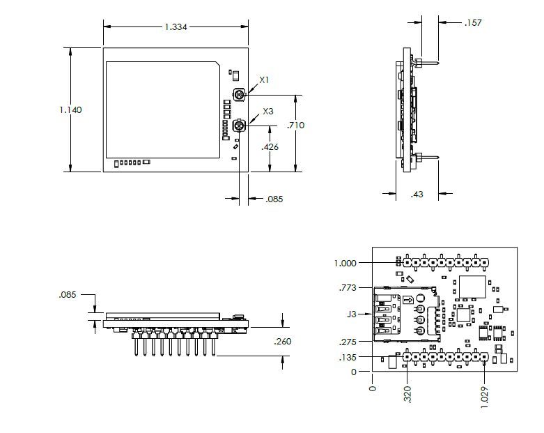
Table of Contents
Table of Contents                                                               2

Introduction                                                                    4
    Scope                                                                       4
    Contact Information                                                         4
    Orderable Part Numbers                                                      4
    Additional Resources                                                        4
    Product Overview                                                            5
    Block Diagram                                                               5

Technical Specifications                                                         6
   Electrical Specifications                                                     6
      Absolute Maximum Ratings                                                   6
      Typical Power Consumption                                                  6
      Module Pinout for Connectors J1 and J2                                     7
      Module Pinout for Connectors J3, X1, X3                                    9
   RF Specifications                                                             9
   Mechanical Specifications                                                    10
      Mechanical Characteristics                                                10
      Mechanical Drawing                                                        10
      Mating Connectors                                                         11
      Device Placement                                                          11
      Environmental Specifications                                              11

Design Considerations                                                           12
  Power Supply Requirements                                                     12
     Power Supply Design Guidelines                                             13
  Serial Communications                                                         14
     Serial UART Interface                                                      14
     USB Interface                                                              14
  VREF                                                                          14
  Power Control                                                                 15
     ON_OFF Signal                                                              15
     Power Monitoring                                                           16
     Shutdown                                                                   16
  Firmware Updates Over the Air (FOTA)                                          17
  Soldered-Down SIM                                                             17
  GNSS                                                                          18
  PN 1001722 rev 8           © NimbeLink Corp. 2019. All rights reserved.   2
GNSS Antenna Requirements                                               18
      Active GNSS Antenna Control                                             19
      GNSS Antenna Placement                                                  19
      Recommended Antennas                                                    19
   Cellular Antenna Requirements                                              20
      Primary Antenna Requirements                                            20
      Antenna Placement                                                       21
      Recommended Antennas                                                    21
   Skywire Reference Design                                                   21

Mounting Guidelines                                                           22
  Board-to-Board Connectors Approach                                          22
     Mechanical Retention                                                     22
  Solder to Board Connection                                                  23

Regulatory information                                                        23
  Carrier Specific Certifications                                             23
  Export Control Classification Number (ECCN)                                 23
  RoHS Compliance                                                             24
  Interference statement                                                      24
  FCC & IC Compliance                                                         24
  Wireless Notice                                                             25
  Modification Statement                                                      25
  End Product Labeling Requirements                                           25

  PN 1001722 rev 8         © NimbeLink Corp. 2019. All rights reserved.   3
1. Introduction
1.1 Scope
The aim of this document is to serve as a hardware reference datasheet for the
NL-SW-LTE-QBG96 Skywire® modem family.
1.2 Contact Information
NimbeLink’s goal is to make integrating the Skywire modem into your product as easy
as possible. Please send any feedback, documentation requests, or technical support
questions to Nimbelink’s product support team at:
product.support@nimbelink.com
For purchasing information, please visit the "Part Ordering Information" section on the
modem’s product page. Any additional sales questions or requests for quotation can be
directed to NimbeLink’s sales team at:
sales@nimbelink.com
1.3 Orderable Part Numbers
Operating Applicable
Orderable Device 4G LTE Bands Fallback?
Temperature Networks
LTE-FDD: B1, B2 B3, B4, AT&T, Orange,
2G GSM:
B5, B8, B12, B13, B18, Telstra, Telus,
GSM850,
B19, B20, B26, B28 T-Mobile,
NL-SW-LTE-QBG96 -40 to +85˚C GSM900,
Verizon,
DCS1800,
LTE-TDD: B39 Vodafone,
PCS1900
(LTE-M only) And more
1.4 Additional Resources
● Skywire® Global 4G LTE Cat M1 Embedded Modem Product Page
● Skywire® Global 4G LTE Cat M1 AT Command Manual
● Skywire® Global 4G LTE Cat M1 Application Notes
● 4G LTE Cat M1 Skywire NL-SWDK User Manual
● Skywire Hardware Design Developers Guide
● Skywire Hardware Design Checklist
● Skywire Software Developers Guide
PN 1001722 rev 8 © NimbeLink Corp. 2019. All rights reserved. 41.5 Product Overview The Skywire® Global 4G LTE Cat M1 embedded modem is purpose-designed for IoT applications, particularly those requiring location-based functionality. Based on the Quectel BG96 module, it has full FCC, IC, and carrier end-device certifications, which can save users months of testing and tens of thousands of dollars in cost. Like all Skywire modems, the QBG96 is among the smallest embedded modems in the industry, and is compatible with a wide range of Skywire development kits and microprocessor shields, helping to accelerate product development and prototyping. LTE Cat M1 modems have the lowest power requirements of any cellular modem type, making them ideal for battery operated, mobile, or off-grid applications. Depending on the application, they may be able to run for years unattended and without requiring a battery replacement or recharge. 1.6 Block Diagram PN 1001722 rev 8 © NimbeLink Corp. 2019. All rights reserved. 5
2. Technical Specifications
      2.1 Electrical Specifications
      2.1.1 Absolute Maximum Ratings

                               Parameter              Signal         Maximum Rating
                           Main Power Supply           VCC                 4.3V
                          I/O Voltage Reference       VREF                 5.5V

      2.1.2 Typical Power Consumption

                    Signal                        Average       Peak     Average
    Mode         Attenuation    RSRQ     RSRP     Current      Current   Charge          Measurement Notes
                     (dB)                          (mA)         (mA)      (µAh)
                                                                                       Tested at 3.8V
Active Socket                                                                          Time elapsed: 20.474s
Dial - Normal         0           12       65     70.6492      339.977   408.524       Test: Open socket, HTTP
     SIM                                                                               POST, read HTTP
                                                                                       response, power off

                                                                                       Tested at 3.8V
Active Socket                                                                          Time elapsed: 20.740s
Dial - Normal        20           13       50     71.184       359.832   414.546       Test: Open socket, HTTP
     SIM                                                                               POST, read HTTP
                                                                                       response, power off

                                                                                       Tested at 3.8V
Active Socket                                                                          Time elapsed: 20.653s
Dial - Normal        40           13       26     75.193       625.849   435.851       Test: Open socket, HTTP
     SIM                                                                               POST, read HTTP
                                                                                       response, power off

                                                                                       Tested at 3.8V
 Active Socket                                                                         Time elapsed: 44.720s
     Dial -           0           15       65     57.455       337.342   714.196       Test: Open socket, HTTP
Integrated SIM                                                                         POST, read HTTP
                                                                                       response, power off

                                                                                       Tested at 3.8V
 Active Socket                                                                         Time elapsed: 45.301s
     Dial -          20           15       50     58.314       409.365   734.491       Test: Open socket, HTTP
Integrated SIM                                                                         POST, read HTTP
                                                                                       response, power off

           PN 1001722 rev 8             © NimbeLink Corp. 2019. All rights reserved.                 6
Signal Average Peak Average
Mode Attenuation RSRQ RSRP Current Current Charge Measurement Notes
(dB) (mA) (mA) (µAh)
Tested at 3.8V
Active Socket Time elapsed: 43.868s
Dial - 40 14 26 60.932 570.067 743.264 Test: Open socket, HTTP
Integrated SIM POST, read HTTP
response, power off
Tested at 3.8V
6.474 301.26 551.336 Issued AT+CFUN=0,
Off 0 12 64
(uA) (uA) (nAh) AT+QPOWD, 5 minute
sample
Tested at 3.8V
Powered on and registered
Idle 0 15 64 61.862 354.820 2817.362
on the network, 5 minute
sample
12.310 406.448 286.584 Tested at 3.8V
PSM 0 16 65
(uA) (uA) (nAh) PSM State, 289s sample
2.1.3 Module Pinout for Connectors J1 and J2
The following table details the pinout of the NL-SW-LTE-QBG96 Skywire modem, and
recommended ratings for the Skywire interface on connectors J1 and J2. Further details
and design requirements for these pins are documented in Section 3.
Pin Name Direction Description Min Typ. Max If not used
1 (J1-1) VCC Input Main Power supply 3.4V 3.8V 4.3V Must be implemented
UART data out, I/O level tied Must be implemented if
2 (J1-2) DOUT Output 0V VREF
to VREF USB not used
VREF Range VIL VIH
VREF x VREF x
1.65V to 1.95V
UART 0.35V 0.65
data in,
2.3V to 2.7V 0.7V 1.7V Must be implemented if
3 (J1-3) DIN Input I/O level
USB not used
tied to
VREF 3.0V to 3.6V 0.8V 2V
VREF x VREF x
4.5V to 5.5V
0.3V 0.7
4 (J1-4) GND Input Ground Pin 0V Must be implemented
VIL: VIH:
Reset signal for the Quectel
5 (J1-5) nRESET Input GND to 1.3V to No connection
BG96 module
0.5V 2.1V
6 (J1-6) VUSB Input USB connection detection 3.0V 5.0V 5.25V No connection
PN 1001722 rev 8 © NimbeLink Corp. 2019. All rights reserved. 7Pin Name Direction Description Min Typ. Max If not used
USB differential data bus (+) Compliant with
7 (J1-7) USB_P I/O Requires differential USB 2.0 standard No connection
impedance of 90Ω. specification.
USB differential data bus (-) Compliant with
8 (J1-8) USB_N I/O Requires differential USB 2.0 standard No connection
impedance of 90Ω. specification.
Data terminal ready (sleep VIL: VIH:
9
mode control), tied to internal GND to 1.35V
(J1-9)
DTR Input reference voltage of 1.8V 0.45V to 5.5V No connection
10
GND Input Ground Pin 0V Must be implemented
(J1-10)
11
GND Input Ground Pin 0V Must be implemented
(J2-1)
12
CTS Output Clear to send 0V VREF No connection
(J2-2)
Indicates the current
13 operation status of the BG96
STATUS Output 0V 1.8V No connection
(J2-3) module. Driven high when the
module is on.
1.8V
14 Voltage reference for offboard
VREF Input 0V or 5.5V Must be implemented
(J2-4) I/O signals.
3.3V
15
GND Input Ground Pin 0V Must be implemented
(J2-5)
VREF Range VIL VIH No connection
Modem
"Request VREF x VREF x
1.65V to 1.95V
to Send" 0.35V 0.65
16
RTS Input hardware 2.3V to 2.7V 0.7V 1.7V
(J2-6)
flow
control 3.0V to 3.6V 0.8V 2V
input VREF x VREF x
4.5V to 5.5V
0.3V 0.7
17 I2C serial data. Used for
I2C SDA I/O Pulled up to 1.8V internally No connection
(J2-7) external codec.
18 I2C serial clock. Used for
I2C SCL I/O Pulled up to 1.8V internally No connection
(J2-8) external codec.
Ring Indicator Output.
Normally high, 120ms low VOL
19
RING Output pulse when URC present. 0 to VREF No connection
(J2-9)
Open Drain output, 1M pull-up 0.1V
on modem.
Modem On/Off signal. See
20 1.3V ≤ VIH ≤ 2.1V
ON_OFF Input Section 3.5 for additional Must be implemented.
(J2-10) 0V ≤ VIL ≤ 0.5V
requirements.
Additional information on the Skywires pinout is available in Section 3.
PN 1001722 rev 8 © NimbeLink Corp. 2019. All rights reserved. 82.1.4 Module Pinout for Connectors J3, X1, X3
Connector Designator Description Connector Location
J3 Micro SIM Connector Bottom Side of Modem
X1 Primary Cellular Antenna Connection Top side of Modem
X3 GPS/GNSS Satellite Receiver Top Side of Modem
2.2 RF Specifications
Parameter Value
4G LTE Technology 4G Cat M1, 4G Cat NB1
4G LTE TX output power 23dBm ± 2dB
Band Cat M1/3GPP (dBm)
B1 -107.0/-102.7
B2 -106.7/-100.3
B3 -106.8/-99.3
B4 -106.9/-102.3
B5 -107.0/-100.8
4G LTE RX
Sensitivity B8 -107.3/-99.8
B12 -107.7/-99.3
B13 -106.5/-99.3
B18 -107.5/-102.3
B19 -107.1/-102.3
B20 -107.2/-99.8
B26 -107.1/-100.3
B28 -107.2/-100.8
B39 TBD /-103
GSM RX GSM850/GSM900 -109/-102
Sensitivity DCS1800/PCS1900 -108.5/-102
Connection Type Downlink Uplink
Peak Uplink and 4G LTE Cat M1 300 Kbps 375 Kbps
Downlink
4G Cat NB1 32 Kbps 70 Kbps
Speeds
GSM 296 Kbps 236.8 Kbps
PN 1001722 rev 8 © NimbeLink Corp. 2019. All rights reserved. 92.3 Mechanical Specifications
2.3.1 Mechanical Characteristics
Parameter Typical Unit
Dimensions (excluding pin height, for solder to board 29.0 x 33.60 x
mm
applications) 6.63
Dimensions (including pin height, for board to board 29.0 x 33.60 x
mm
connector applications) 10.73
Weight 8 Grams
Connector Insertion/Removal hundreds Cycles
2.3.2 Mechanical Drawing
PN 1001722 rev 8 © NimbeLink Corp. 2019. All rights reserved. 102.3.3 Mating Connectors
Connector Populated on Recommended Mate Manufacture
Manufacturer
Designator Modem Mate
950510-6102-AR 3M
J1, J2 3M Acceptable
951110-2530-AR-PR Sullins Connector
alternate:
Solutions
NPPN101BFCN-RC
J3 Molex 786463001 Micro SIM 3FF Size Micro SIM Card
X1, X3 Hirose U.FL-R-SMT(10) CAB.011 Taoglas
2.3.4 Device Placement
⚠ Make sure the Skywire is installed in the correct orientation in your host
board; failure to do so will damage the device and void the warranty.
2.3.5 Environmental Specifications
Parameter Min Typical Max Unit Note
Operating
-40 25 +85 ˚C
Temperature
Storage
-40 25 +90 ˚C
Temperature
Operating Humidity 20 90 % Non-condensing
PN 1001722 rev 8 © NimbeLink Corp. 2019. All rights reserved. 113. Design Considerations
The following sections detail various design considerations that system designers
should follow when designing the Skywire modem into their system. NimbeLink offers
free schematic and layout design reviews for customers integrating a Skywire modem
into their design. For more details please reach out to Nimbelink product support team
at product.support@nimbelink.com.
3.1 Power Supply Requirements
NL-SW-LTE-QBG96 modems will regularly consume high amounts of current on its
Main Power Supply (Pin 1, VCC) input, up to 1.2A during LTE-M1 transmits and
receives, 2G GSM connections will repeatedly hit 2A during transmissions. In order to
maintain compatibility with other 4G Skywire modems, the baseboard power supply
should be designed to support peak currents of at least 2 Amps. A 0.1 uF & 100uF low
ESR ceramic capacitor should be placed on the baseboard near the VCC pin of the
Skywire to ensure ample energy is available, with a low inductance path to the VCC pin.
Parameter Value
Nominal Supply Voltage 3.8V
Operating Voltage Range 3.40V to 4.30V
Extended Operating Voltage Range 3.20V to 4.50V
NL-SW-LTE-QBG96 modems have a normal operating voltage range of 3.40V to 4.30V,
with a recommended input voltage of 3.80V. The modems also support an extended
operating voltage range of 3.20V to 4.50V. Extreme care must be taken when operating
the modem outside of the standard operating voltage range of 3.40V to 4.30V.
If there is a voltage drop or overshoot that exceeds the limits of the extended operating
voltage range, it may cause damage to the modem and void the modem’s warranty. The
extended operating voltage range should only be used with thoroughly tested power
supply systems that have been shown to be able to handle the rigorous current
demands of an LTE modem without falling out of the extended operating voltage range.
PN 1001722 rev 8 © NimbeLink Corp. 2019. All rights reserved. 123.1.1 Power Supply Design Guidelines
When designing the power supply for a Skywire modem it is recommended to adhere to
the following design guidelines:
● For most applications, a switching power supply is recommended to supply
power to the Skywire modem. This is because switching power supplies are
able to rapidly respond to the sudden current demands of an LTE modem. To
ensure compatibility with other Skywire modems, it is recommended to use a
switching regulator capable of supporting up to 2A. Example designs using a
switching DC/DC regulator can be found in the reference schematics below.
● To reduce EMI from the switching regulator, it is important to follow the design
guidelines from the device manufacturer.
● Bypass ceramic capacitors (low ESR) with adequate capacity must be placed
near the input to pin 1 (VCC) of the Skywire modem. It is recommended that
the capacitor have a rated voltage of at least 2x the input voltage to the
Skywire. A minimum of a 100 uF & 0.1uF capacitor is recommended for all
Skywire modems. The 0.1uF capacitor should be placed as close as possible
to pin 1 of the Skywire modem, followed by the 100 μF capacitor.
● The PCB traces from the power regulator and the bypass capacitors must be
at least 80 mils to ensure that there is a low impedance power delivery circuit
available to the modem. This ensures that no significant voltage drops occur.
Try to keep the trace as short as possible.
● A dedicated ground plane is recommended.
● Power supply input cables should be kept away from noise sensitive lines,
such antennas.
NimbeLink offers multiple power supply reference designs in order to assist customers
with their designs at no extra charge. Two of the designs are linked to below:
NL-AB-BBCL Reference Schematic
NL-SWDK Reference Schematic
Nimbelink highly recommends prototyping with a Skywire Development kit as opposed
to a breadboard, which will not work with a Skywire modem. Please refer to the
following application note, which explains this incompatibility in more detail:
Prototyping with Cellular Modems and Modules
PN 1001722 rev 8 © NimbeLink Corp. 2019. All rights reserved. 133.2 Serial Communications
The NL-SW-LTE-QBG96 modem has two communication paths: serial (UART) and
USB. The serial UART interface is targeted for applications using lower speed 8/16/32
bit microcontrollers that do not have a USB interface or easily available USB interface
drivers. The USB interface for the modem is meant for use by higher end systems with
a native USB interface controller or operating system (Single board computers,
Linux/Windows).
For designs that are only using the serial UART interface, NimbeLink recommends
designers include test points or a non-populated USB connector footprint in their
designs. This allows access to the modem’s USB interface to enable easy debugging
and firmware updates.
3.2.1 Serial UART Interface
All Skywire modems support a serial UART interface with transmit and receive on pins 2
(DOUT) and 3 (DIN). On the NL-SW-LTE-QBG96 modem, the baud rate defaults to
115200 Baud 8N1. If a different baud rate is required, it can be changed with the
AT+IPR command as defined in the AT command manual. The modem also supports
RTS/CTS flow control on pins 12 (CTS) and 16 (RTS).
By default, the modem does have flow control enabled. To modify the flow control
setting, please see the AT+IFC command in the AT command manual. It is
recommended that any designs using the serial UART interface connect the RTS/CTS
flow control lines to the host microcontroller and enable them in their application.
3.2.2 USB Interface
The NL-SW-LTE-QBG96 modem supports a USB 2.0 interface on pins 6 (VUSB), 7
(USB_P), and 8 (USB_N). Systems connecting to the modem’s USB interface must
observe proper design practices for connecting to a high speed USB device including,
but not limited to, the following:
● The USB D± traces should be routed as a 90 ohm impedance differential pair.
● The USB D± traces should length matched.
● USB trace lengths should be minimized.
● USB differential pairs should be carefully routed to ensure they have a
continuous return path beneath the traces. Do not route differential pairs over
splits in ground or power planes.
● If the USB signals will be used off-board, ESD protection should be implemented
near the off-board connector.
Pin 6 is the VUSB detection pin that the modem uses to detect if a USB host controller
has been connected to the modem. This pin has an internal pulldown and must have a
voltage between 3.0V and 5.5V applied to it in order to activate the USB interface. The
VUSB pin will draw less than 5mA when connected. VUSB must be disconnected or
asserted to ground before activating Power Saving Mode.
PN 1001722 rev 8 © NimbeLink Corp. 2019. All rights reserved. 143.3 VREF Th VREF signal drives the input voltage side of an onboard buffer which converts external I/O voltage from the VREF range to the 1.8V range in order to drive the onboard Quectel BG96 module. System designers should connect the reference voltage of their system to this pin. The VREF signal will draw less than 1mA when the modem is powered. To enable low power operation, system designers should include a method of removing the voltage from VREF when the system is in Power Save Mode (PSM). One such method would be to power VREF from a GPIO or to have a P-CH MOSFET in the VREF signal path. 3.4 nRESET Signal In the event that the modem becomes unresponsive, pin 5 (nRESET) can be grounded to unconditionally shut down the modem. When pin 5 is grounded, the modem will cease all ongoing operations, and reset itself. Please note: the modem will not detach itself from the network before resetting. Network providers request that a device gracefully detach from the network before shutting down. Accordingly, this functionality should only be used as an emergency reset when the modem is not responding to commands. To unconditionally shut down the modem with the nRESET signal, tie the pin low for at least 150 ms, and then release. The signal is internally pulled up to the modem’s internal 1.8V rail. If the signal is unused, it can be left floating, but it is highly recommended that the signal be connected to the host system. If the signal is used, it should be driven with an open collector output from the host system or a discrete open collector transistor. In high noise (high EMI) environments, we recommend designers place a 0.01-0.1 uF capacitor on the nRESET line near the J1 connector. 3.5 Power Control 3.5.1 ON_OFF Signal The ON_OFF signal on pin 20 is used to trigger the modem to turn on, and to turn the modem off. Please note: do not power this pin nor apply a pullup resistor. To conserve power, the onboard cellular module does not automatically startup when power is applied. Therefore, the baseboard design must supply a means to assert a logic-low level on the ON_OFF pin. To initiate the startup procedure, tie ON_OFF to ground for at least 100 ms. Similarly, if the modem is currently running, the ON_OFF pin can be pulled low for at least 650 ms to initiate a power-down sequence. The ON_OFF signal should be driven with an open collector output or with an open collector transistor. The signal is internally pulled up and should not be driven high, as doing so may prevent the modem from booting. PN 1001722 rev 8 © NimbeLink Corp. 2019. All rights reserved. 15
Additionally, the module can be configured to automatically start when power is applied.
This can be done by tying the ON_OFF signal to GND (either directly or through a
pulldown resistor). However, doing so does run the risk of the modem attempting to
boot before the input voltage to the modem is >3.20V, which could cause the modem to
lock up. If lock up occurs, the nRESET pin should be asserted to force the modem to
initiate a restart.
For optimal control of the cellular modem, it is recommended that the system designer
control the ON_OFF signal from their host platform using an open collector output or
external discrete open collector transistor.
3.5.2 Power Monitoring
Applications can check to see if the modem has powered up by reading the logic state
on pin 13 (STATUS). When the Quectel BG96 module is powered up and running, pin
13 will be driven high to 1.8 V. When the module is not running, this pin will be
grounded.
3.5.3 Shutdown
The modem should be shut down in a controlled manner, so as to gracefully disconnect
it from the network. Failure to do so violates carrier requirements. In rare events, failure
to properly shut down the modem could render the modem inoperable due to firmware
corruption.
To gracefully shut down the modem, the host system should do the following:
● Shut down the modem with the AT+QPOWD=1 command. This command will
gracefully disconnect the modem from the network and shut down the modem.
This process will take no longer than a couple of seconds. After this command is
issued, the host system should cease any communications with the modem.
● If power is to be cut from the modem, ensure that the host system is not back
powering the modem through any of the modem’s I/O lines.
● Users should monitor the STATUS pin (as described in Section 3.5.2) to ensure
the modem has powered down.
● Remove VREF (if VCC is being removed).
● Remove VCC.
In the event of power failure, the modem may need to be shut down faster than the
AT+QPOWD=1 command can manage. To immediately power down the modem in the
event of power failure, the AT+QPOWD=0 command can be used to force a fast shutdown.
PN 1001722 rev 8 © NimbeLink Corp. 2019. All rights reserved. 163.6 Network Status Monitoring
In order to conserve power, the NL-SW-LTE-QBG96 does not have a status LED. It is
recommended to monitor the modem’s network status using AT commands and the
serial interface.
3.7 Firmware Updates Over the Air (FOTA)
LTE networks are constantly being updated, improved, and enhanced with new
features. As a result, carriers are making frequent network changes. Most will not
negatively affect devices connected to those networks, but occasionally an update will
prevent an unprepared device from reconnecting to the network permanently.
To account for these future changes, FOTA (Firmware over the Air) capability is being
added to cellular modules by each manufacturer. Accordingly, NimbeLink supports this
functionality in the entire Skywire family of embedded modems. As such, it is highly
recommended that designers implement provisions to accommodate for FOTA
processes.
Failure to accommodate FOTA processes may result in interruptions in cellular
connectivity in the event of network changes. If a device can no longer access the
network, FOTA cannot be used to remedy the problem. The only way to recover
functionality is to physically update the device firmware.
FOTA Instructions are available by contacting NimbeLink's product support team at
product.support@nimbelink.com.
3.8 Soldered-Down SIM
The NL-SW-LTE-QBG96 modem has the ability to select between a soldered-down
SIM or a removable SIM inserted into the SIM card slot on the modem.
By default, the modem is configured to attempt to use the SIM card slot. However, users
can select which SIM the modem is using by controlling the onboard SIM selection
switch with AT commands. Whenever SIM selection is switched, the modem’s RF
system will need to be toggled with the AT+CFUN command.
To configure the modem to use the soldered down SIM issue the following commands
to the modem in the order they appear below:
AT+CFUN=0
AT+QCFG="gpio",1,26,1,0,0,1
AT+QCFG="gpio",3,26,1,1
AT+CFUN=1
PN 1001722 rev 8 © NimbeLink Corp. 2019. All rights reserved. 17To configure the modem to use the SIM in the SIM card socket issue the following
commands to the modem in the order they appear below:
AT+CFUN=0
AT+QCFG="gpio",1,26,1,0,0,1
AT+QCFG="gpio",3,26,0,1
AT+CFUN=1
Note: GPIO states will persist after reset, and the above AT commands will not need to
be reissued each time the modem is powered on. Firmware updates may overwrite
saved GPIO states, however.
3.9 GNSS
The onboard Quectel BG96 module includes a fully integrated global navigation satellite
system solution that supports Gen8C-Lite of Qualcomm (GPS, GLONASS,
BeiDou/Compass, Galileo and QZSS). The BG96 has an embedded low-noise amplifier
(LNA) that is utilized by the GNSS system. The modem supports both passive GNSS
antennas and active antennas with a gain, at the modems RF connector, of 0 dBi
Active Antenna Noise Figure < 1.5 dBi
Active Antenna Gain > -2 dBi
Active Antenna External LNA Gain 20 dB (Maximum)
Active Antenna Total Gain < 18 dBi
GNSS Frequency Frequency
GPS/Galileo/QZSS 1575.42 ± 1.023 MHz
GLONASS 1597.5 - 1605.8 MHz
BeiDou 1561.098 ± 2.046 MHz
PN 1001722 rev 8 © NimbeLink Corp. 2019. All rights reserved. 183.9.2 Active GNSS Antenna Control
A 3.3VDC, 100 mA source is available on the modem to bias the GPS line in order to
power the modem. Control of the GNSS power source is done via GPIO64 on the
modem. To conserve power, the GNSS power is off by default.
To turn on the DC power to the GNSS antenna, and save it in this state across power
off, issue the following commands to the modem:
AT+QCFG="gpio",1,64,1,0,0,1
AT+QCFG="gpio",3,64,1,1
To turn off the DC power to the GNSS antenna, and save this state after power off,
issue the following commands to the modem:
AT+QCFG="gpio",1,64,1,0,0,1
AT+QCFG="gpio",3,64,0,1
Note: GPIO states will persist after reset, and the above AT commands will not need to
be reissued each time the modem is powered on. Firmware updates may overwrite
saved GPIO states, however.
3.9.3 GNSS Antenna Placement
● The antenna must be installed according to the antenna manufacturer’s
instructions in order to obtain the maximum performance of the GNSS
receiver.
● The antenna location must be evaluated carefully if operating in conjunction
with any other antenna or transmitter.
● The antenna must not be installed inside metal cases or near any obstacle
that may degrade features like antenna lobes and gain.
● Keep the antenna and the antenna cabling away from any power supply lines,
noisy EM devices, and wireless RF lines.
3.9.4 Recommended Antennas
Type Manufacturer Part Number
1
GPS/GALILEO Antenna, Internal Taoglas AP.17E.07.0064A
1
GPS/GALILEO Antenna, External Taoglas AA.108.301111
Note 1: U.FL to SMA adapter required.
PN 1001722 rev 8 © NimbeLink Corp. 2019. All rights reserved. 193.10 Cellular Antenna Requirements
NL-SW-LTE-QBG96 modems support one primary cellular antenna connection for RX &
TX communication via the X1 connector on the top of the modem. The X1 connector is
a U.FL connector. Many antennas will require the use of a U.FL to SMA cable, such as
the Taoglas CAB.011.
3.10.1 Primary Antenna Requirements
Depending on the frequency band(s) provided by the network operator, the customer
shall use the most suitable antenna for that/those band(s):
Item Value
Band Uplink (MHz) Downlink (MHz)
B1 1920 – 1980 2110 – 2170
B2 1850 – 1910 1930 – 1990
B3 1710 – 1785 1805 – 1880
B4 1710 – 1755 2110 – 2155
B5 824 – 849 869 – 894
B8 2500 – 2570 2620 – 2690
B12 699 – 716 729 – 746
Frequency Range
B13 777 – 787 746 – 756
B18
B19 830 – 845 875 – 890
B20 832 – 862 791 – 821
B26 814 – 849 859 – 894
B28
B39 1880 - 1920
VSWR < 2 (Typ.)
Gain 1 dBi
Impedance 50 Ω
Polarization Vertical
Cable Insertion Loss
(LTE B5/B8/B12/B13/B18/B19/B20/B26/B28 < 1 dBi
GSM850/GSM900)
Cable Insertion Loss
< 1.5 dBi
(LTE B1/B2/B3/B4/B39, DCS1800/PCS1900)
Note: Any antennas used with the modem will need to comply with the Wireless Notice detailed
in Section 5.7.
PN 1001722 rev 8 © NimbeLink Corp. 2019. All rights reserved. 203.10.2 Antenna Placement
The modem’s cellular antenna placement will directly affect the modem’s performance.
It is vital that system designers carefully consider the placement of the antenna and
follow all of the guidelines & specifications set by the antenna manufacturer. The
following guidelines are general recommendations for antenna installation:
● Make sure the antenna has an impedance of 50 ohms.
● Keep the antenna cable as short as possible.
● The antenna must not be installed inside a metal enclosure, nor near metal
objects unless specified by the antenna manufacturer.
● The antenna must be installed according to the manufacturer's instructions.
● Antenna gain must not exceed the values indicated in the regulatory
requirements.
● Antenna integration should optimize antenna efficiency. Antennas are
recommended to have >50% efficiency on all frequency bands.
● Additional FCC/IC testing may be required for applications where the antenna is
located closer than 20 CM from the body.
● If the device antenna is located farther than 20cm from the human body and
there are no co-located transmitter, the Quectel FCC/IC approvals can be
re-used by the end product
● Antenna should not be mounted near noisy EM devices.
3.10.3 Recommended Antennas
Type Manufacturer Part Number
Internal Cellular Antenna Taoglas FXUB65.07.0180C
1
External Cellular Antenna Taoglas TG.30.8113
Note 1: U.FL to SMA adapter required.
3.11 Skywire Reference Design
NimbeLink offers free reference schematic and layout files as examples of how to
integrate Skywire modems into various systems. Schematics, design files, gerber files,
and tutorials for a variety of different systems can be found on the Skywire Development
Tools webpage.
PN 1001722 rev 8 © NimbeLink Corp. 2019. All rights reserved. 214. Mounting Guidelines Skywire embedded cellular modems support multiple connection methods. The two primary methods are board-to-board connectors and soldering directly to the baseboard. 4.1 Board-to-Board Connectors Approach The Skywire interface calls for two 10-pin, 2mm pitch, female receptacles spaced 22 mm apart. There are many connector manufacturers that can be used. Below is one readily available product: Manufacturer: Sullins Connector Solutions, Part Number: NPPN101BFCN-RC Typical part drawing and footprint information for the NPPN101BFCN-RC connector: When using the recommended connector, ensure that any baseboard components placed under the Skywire (between the baseboard header pin connectors) are no taller than 4 mm. However, please note that the maximum component height may change based on the chosen baseboard connector. 4.1.1 Mechanical Retention Certain applications where the modem is mounted on the host board using the connector approach detailed in section 4.1 may need to mechanically secure the Skywire modem & its SIM card in order to prevent the modem from vibrating out of the mating connectors. Skywire modems do not have any dedicated attachment points for securing to the host board, however it can easily be secured by one of the following methods: ● Zip ties ● Foam tape mounted on the Skywire to press against the enclosure ● Mechanical retention of the modem & SIM by the enclosure (example) ● Solder the Skywire to the host board (as described in Section 4.2) PN 1001722 rev 8 © NimbeLink Corp. 2019. All rights reserved. 22
4.2 Solder to Board Connection Alternatively, Skywires can be soldered directly to a PCB. The PCB should be designed with two rows of ten 0.8mm plated through holes spaced 2mm apart. See the figure below for the recommended footprint. Note: All measurements are in millimeters. U.FL connectors X1 and X3 are on the top side of the board. Micro SIM card slot J3 is on the bottom of the board. When using soldering directly to a PCB, ensure that any baseboard components placed under the Skywire (between the baseboard header pin connectors) are no taller than 0.5 mm. 5. Regulatory information 5.1 Carrier Specific Certifications NL-SW-LTE-QBG96: Verizon ODI, PTCRB, AT&T, GCF, Telus, Orange 5.2 Export Control Classification Number (ECCN) ECCNs are five character alphanumeric designations used on the Commerce Control List (CCL) to identify dual-use items for export control purposes. An ECCN categorizes items based on the nature of the product, i.e. type of commodity, software, or technology and its respective technical parameters. ECCN for All Skywire Modems: 5A992.c PN 1001722 rev 8 © NimbeLink Corp. 2019. All rights reserved. 23
5.3 Harmonized Tariff Schedule Code HTS Code: 8517.62.0010 5.4 RoHS Compliance The NL-SW-LTE-QBG96 modem family complies with the RoHS (Restriction of Hazardous Substances) directive of the European Union, EU Directive 2011/65/EU. 5.5 Interference statement This device complies with Part 15 of the FCC Rules and Industry Canada licence-exempt RSS standards. Operation is subject to the following two conditions: (1) This device may not cause harmful interferences, and (2) this device must accept any interference received, including interference that may cause undesired operation. 5.6 FCC & IC Compliance If the modem’s antenna is located farther than 20cm from the human body and there are no adjacent transmitters, the FCC/IC approvals of the on-board Quectel BG96 cellular module can be reused by the end product. Should the modems antenna be mounted closer than 20cm from the human body or if there are adjacent transmitters, additional FCC/IC testing may be required for the end product. NL-SW-LTE-QBG96 modems make use of the on-board Quectel module’s FCC & IC identification numbers. Orderable Device FCC ID IC ID (certification number) NL-SW-LTE-QBG96 XMR201705BG96NA 10224A-201709BG96 The FCC certificate is available at the following link by searching for the FCCID listed above: https://www.fcc.gov/oet/ea/fccid The IC ID certificate is available at the following link by searching for the IC ID listed above: https://sms-sgs.ic.gc.ca/equipmentSearch/searchRadioEquipments?execution=e1s1&la ng=en PN 1001722 rev 8 © NimbeLink Corp. 2019. All rights reserved. 24
5.7 Wireless Notice
In order to maintain FCC/IC radiation exposure limits set forth for an uncontrolled
environment alongside carrier specific certifications the antennas cannot exceed the
maximum gain levels listed here:
Band Max Antenna Gain
GSM 850 4 dBi
GSM 1900 4 dBi
Band 2 4 dBi
Band 4 4 dBi
Band 5 4 dBi
Band 12 4 dBi
Band 13 4 dBi
5.8 Modification Statement
Nimbelink has not approved any changes or modifications to this device by the user.
Any changes or modifications could void the user’s authorization to operate the
equipment.
5.9 End Product Labeling Requirements
End products utilizing NL-SW-LTE-QBG96 modems should be labeled with the following
information:
Device Uses Approved Radio: NL-SW-LTE-QBG96
Contains FCC ID: XMR201705BG96NA
Contains IC: 10224A-201709BG96
This device complies with Part 15 of the FCC Rules and Industry Canada
licence-exempt RSS standards. Operation is subject to the following two
conditions: (1) This device may not cause harmful interferences, and (2) this
device must accept any interference received, including interference that may
cause undesired operation.
PN 1001722 rev 8 © NimbeLink Corp. 2019. All rights reserved. 25You can also read