Snap-3D: A Constrained Placement-Driven Physical Design Methodology for Face-to-Face-Bonded 3D ICs - Pruek Vanna-iampikul, Chengjia Shao, Yi-Chen ...

Page created by Lauren Lucas
 
CONTINUE READING
Snap-3D: A Constrained Placement-Driven Physical Design Methodology for Face-to-Face-Bonded 3D ICs - Pruek Vanna-iampikul, Chengjia Shao, Yi-Chen ...
Snap-3D: A Constrained Placement-
Driven Physical Design Methodology
for Face-to-Face-Bonded 3D ICs

Pruek Vanna-iampikul, Chengjia Shao, Yi-Chen Lu,
Sai Pentapati, and Sung Kyu Lim
Georgia Institute of Technology
Snap-3D: A Constrained Placement-Driven Physical Design Methodology for Face-to-Face-Bonded 3D ICs - Pruek Vanna-iampikul, Chengjia Shao, Yi-Chen ...
Contents
                                                2/16

• Pseudo-3D vs. True-3D physical design flows

• Snap-3D flow
   – Overview
   – Details
   – Strengths

• Experimental Results

• Conclusions
Snap-3D: A Constrained Placement-Driven Physical Design Methodology for Face-to-Face-Bonded 3D ICs - Pruek Vanna-iampikul, Chengjia Shao, Yi-Chen ...
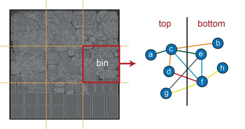
Heterogenous Integration Technologies
                                                  3/16

 2.5D interposer      micro bumping
 TSMC CoWoS           Intel Foveros

 monolithic 3D        hybrid bonding
 coming soon          TSMC SoIC, Samsung X-cube
Snap-3D: A Constrained Placement-Driven Physical Design Methodology for Face-to-Face-Bonded 3D ICs - Pruek Vanna-iampikul, Chengjia Shao, Yi-Chen ...
Pseudo-3D vs. True-3D EDA Tools
                                                                                        4/16

        circuit
                                           1

                                         true-3D
                                       place/route

    2                                                       commercial tool NOT READY

 pseudo-3D
 place/route

                                                     transformation

                  intermediate 2D (commercial tool READY)                  final 3D
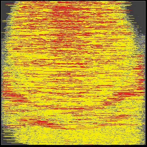
Snap-3D: A Constrained Placement-Driven Physical Design Methodology for Face-to-Face-Bonded 3D ICs - Pruek Vanna-iampikul, Chengjia Shao, Yi-Chen ...
Snap-3D: Overview
                    5/16
Snap-3D: A Constrained Placement-Driven Physical Design Methodology for Face-to-Face-Bonded 3D ICs - Pruek Vanna-iampikul, Chengjia Shao, Yi-Chen ...
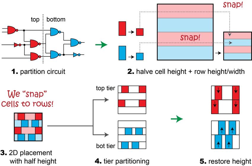
Snap-3D: Design Flow
                                                             6/16

• Goal
   – Use EDA vendor tools as much as possible
   – Then add key missing engines and seamlessly integrate
Snap-3D: A Constrained Placement-Driven Physical Design Methodology for Face-to-Face-Bonded 3D ICs - Pruek Vanna-iampikul, Chengjia Shao, Yi-Chen ...
Our Automatic Tier Partitioner
                                                                                    7/16

• Bin-based hypergraph partitioning
   – Divide 2D into bins, and partition each bin
   – Bi-partitioning engine is Fiduccia-Matheyses algorithm [1982]

     intermediate 2D             hypergraph model        bucket sorting of “gain”

            Why binning? Bin size determines F2F usage!
Snap-3D: A Constrained Placement-Driven Physical Design Methodology for Face-to-Face-Bonded 3D ICs - Pruek Vanna-iampikul, Chengjia Shao, Yi-Chen ...
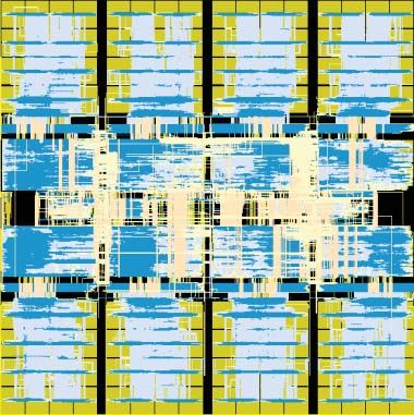
Snap-3D: Key Benefit (1/2)
                                                                               8/16

• Commercial placement quality
   – 2D placement preserved in 3D placement!

         a           b            a        b
             c
                         =                         +           c

                 d                                                 d

    Snap-3D placement         top tier placement       bottom tier placement
Snap-3D: A Constrained Placement-Driven Physical Design Methodology for Face-to-Face-Bonded 3D ICs - Pruek Vanna-iampikul, Chengjia Shao, Yi-Chen ...
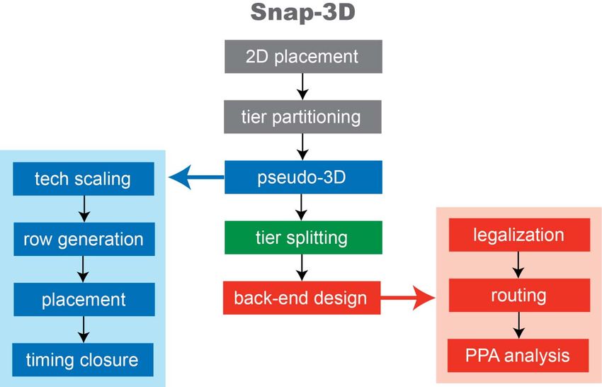
Snap-3D: Key Benefit (2/2)
                                                           9/16

• Commercial routing
  quality
   – We route both tiers
     simultaneously with
     double metal stack

   – This allows metal layer
     sharing!

              connecting cells
              in the bottom tier

              connecting cells
              in the top tier!!!

                                   M5 Bottom   M6 Bottom
Snap-3D: A Constrained Placement-Driven Physical Design Methodology for Face-to-Face-Bonded 3D ICs - Pruek Vanna-iampikul, Chengjia Shao, Yi-Chen ...
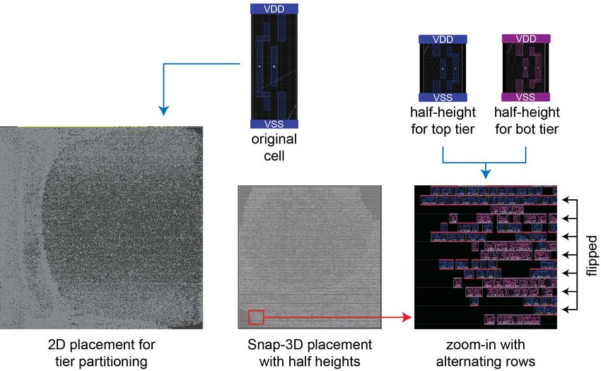
Snap-3D: Placement Sample
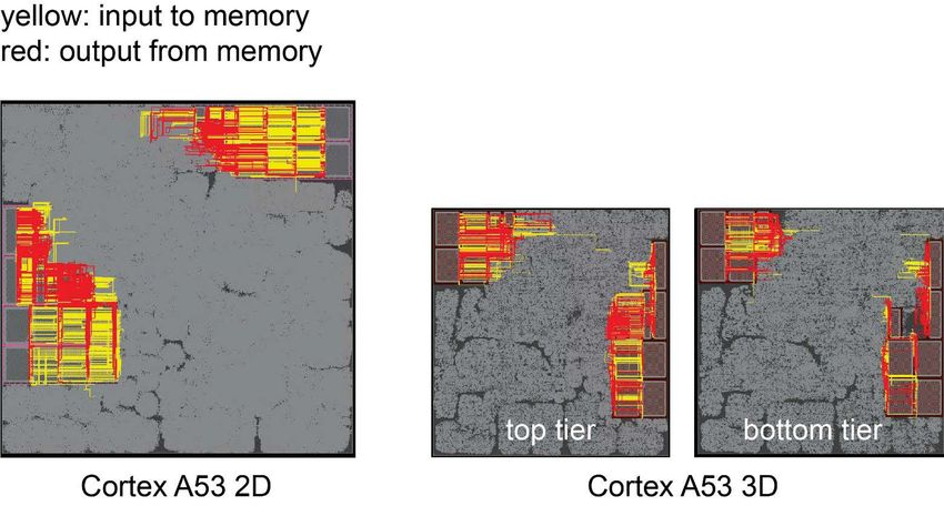
                            10/16
Handling Memory Macros
                                                                     11/16

• Memory macros are used in processor designs
   – Mostly placed manually: become placement blockages in Snap-3D
   – If both tiers are blocked: gate placement not allowed
   – If one tier is blocked: corresponding rows are not used
Full-Chip GDS Layouts
                                                                                12/16

• Snap-3D using TSMC 28nm
   – Not just placement: does routing, timing closure, and PPA simulations
   – High-quality layouts: OUTPERFORMS COMMECIAL 2D PPA

    Cortex A53 2D vs. 3D          Cortex A7 2D vs. 3D       AES_128 2D vs. 3D

        TATE 2D vs. 3D           RocketCore 2D vs. 3D        LDPC 2D vs. 3D
A53 Full-Chip PPA
                                                                                    13/16

                             2D       Shrunk-     Compact-
                                                               Snap-3D
                          Innovus      2D [2]      2D [3]
     target freq (GHz)                          same
     footprint (mm2)         1.0        0.5            0.5        0.5
     # F2F pads               -         1.0            1.01      1.15
     wirelength (m)          1.0       0.69            0.70      0.73
     power (mW)              1.0       0.67            0.66      0.67
     WNS (ns)                1.0       0.57            1.12      0.33
     power × delay          2.10       1.12            1.46      0.97

                Innovus 2D full-chip GDS, A53          Snap-3D full-chip GDS, A53
A53 Memory Latency/Energy
                                                                                  14/16

• Shorter WL in 3D                         metric           2D     3D     3D gain
   – Helps reduce memory         Energy/cycle (pJ)          3.73   2.57    30.8
     access latency and power!   Input latency (max, ps)    209    202      3.4
                                 Input latency (ave, ps)    70     44      37.1
                                 Output latency (max, ps)   272    125     54.0
                                 Output latency (ave, ps)   57     28      50.9
Clock Comparison : AES @ 28nm
                                                                                     15/16

                          2D      Shrunk-     Compact-
     Clock Metrics                                          Snap-3D
                       Innovus     2D [2]      2D [3]
  Clock Latency (ps)     211.8      181.5      177.6         166.1
  Clock Skew (ps)         9.9       11.7        11.3           8.5
  Clock WL. (mm)         43.42      42.15      41.33         38.99
  # Clk. F2F pads          0        674         671           731
  # Clock Buffer          875       910         849           862

             clock tree for AES, 2D Innovus            clock tree for AES, Snap-3D
Conclusions
                                                                                   16/16

• Snap-3D key ideas
   – Use half heights (for cells and rows)
   – Do tier partitioning first and snap cells to rows (= constrained placement)
   – Use double metal stack for routing

• Snap-3D key benefits
   – 2D placement = 3D placement
   – Metal layer borrowing is supported
   – Outperforms Innovus 2D, Shrunk-2D [2] and Compact-2D [3]
You can also read