The photonic opal - the jewel in the crown of optical information processing
←
→
Page content transcription
If your browser does not render page correctly, please read the page content below
FOCUS ARTICLE

                                   www.rsc.org/chemcomm

                                                          The photonic opal – the jewel
                        ChemComm

                                                          in the crown of optical
                                                          information processing
                                                          Photons have many advantages over electrons as carriers of information.They are
                                                          faster and can convey huge amounts of data with low power losses. A new class of
                                                          materials called photonic crystals have the potential to steer light in the same way as
                                                          electrons are manipulated in semiconductor chips. Fabricating these devices is
                                                          proving extremely challenging. Nevertheless, an ingenious chemical approach is
                                                          being exploited by research groups such as that of Geoffrey Ozin at the University
                                                          of Toronto, which may not only contribute to the development of the all-optical
                                                          computer but also stimulate the expansion of a new field of materials science. Nina
                                                          Hall discusses Professor Ozin’s contribution.

                            WHEN it comes to developing new                         photons propagating through a periodic        material exhibiting a regular variation in
                         technologies, a comment often made is                      dielectric can also scatter and interfere,    dielectric constant, or refractive index – a
                         that chemists and physicists need to talk                  resulting in a photonic bandgap. An           photonic crystal (Fig. 1). Yablonovitch’s
                         more. Focused discussion can open up                       appealing aspect is that, unlike the          first effort in 1991 involved simply drilling
                         new scientific vistas glowing with                         Schrödinger equation for interacting          a large-scale 3D array of millimetre-sized
                         potential. This is what Geoffrey Ozin                      electrons in semiconductors, Maxwell’s        air holes in a slab of material with a
                         found when first accosted by his physicist                 equations describing the behaviour of light   refractive index of 3.6. This blocked out
                         neighbour in the lab opposite, Sajeev John.                in periodic dielectric can be solved          light in the microwave region – not
                         To those in the know, Professor John is the                exactly. Furthermore, there is no             particularly practical but it created a
                         world-leading theorist who had, along with                 fundamental scaling length – the              sensation.6
                         Eli Yablonovitch, kicked off the fledgling                 periodicity is not limited to an atomic          To be useful for communications, the
                         field of photonic bandgap crystals –                       lattice and can be on any scale.              spacing of the photonic lattice needs to be
                         materials that are the optical analogues of                   However, nobody had actually created a     comparable with the wavelength of
                         semiconductors. Physicists are excited                     photonic bandgap. What was needed was a       infrared light, at around a micrometre or
                         about them because they could
                         revolutionise telecommunications and put
                         optical computing on a sound footing.
                         John had a precise theoretical blueprint for                   Professor Ozin received a BSc in chemistry
                         making a useful photonic crystal. Ozin,                        from King’s College London and a DPhil in
                         together with Francisco Meseguer in                            inorganic chemistry from the University of
                         Valencia, Spain, had the chemical                              Oxford in 1967. He was ICI Fellow at the
                         experience needed to fabricate it. The                         University of Southampton from 1967 to
                         result was a joint paper in Nature in 2000                     1969 before joining the University of
                         describing the large-scale synthesis of a                      Toronto in 1969; he became full professor in
                         silicon photonic crystal with a complete                       1977 and University Professor in 2001.
                                                                                        Professor Ozin is Honorary Professorial
                         three-dimensional bandgap.2 Three-
                                                                                        Fellow at The Royal Institution of Great
                         dimensional photonic crystals had been
                                                                                        Britain and University College London, and
                         made in silicon using lithography but were                     is a Government of Canada Research Chair
                         just a few periodic layers thick.3                             in Materials Chemistry.
                                                                                           The focus of Professor Ozin’s materials
                         Photonic bandgaps                                              chemistry research is on supramolecular
                         The concept of an optical bandgap was                          chemistry (chemistry beyond the molecule),
                         first proposed in 1987 by Yablonovitch,4                       materials self-assembly over all scales
                         then at Bell Communications in New                             (chemistry approaches to inorganic
DOI: 10.1039/b306771h

                         Jersey, and independently by John,5 then                       materials with complex form), biomimetic
                         at Princeton. The idea somehow seems                           inorganic chemistry (copying the chemistry of
                         obvious now, that – just as the periodic                       biomineralisation), nanochemistry (chemistry at the nanometre scale), inorganic-
                         atomic structure of a semiconductor                            organic hybrid materials (chemistry strategies to nanocomposites), inclusion
                         causes Bragg-like diffraction of                               compounds (host-guest nanomaterials chemistry) and photonic materials chemistry
                         propagating electrons resulting in a                           (chemical approaches to control the flow of light).
                         forbidden range of energies, the bandgap –

                                                                 This journal is © The Royal Society of Chemistry 2003                            CHEM. COMMUN., 2003             2639
structure concept,               between 0.6 and 1 micrometre across,
                                                                                   combined with clever but         made by the base-catalysed hydrolytic
                                                                                   established chemical             polycondensation of
                                                                                   manipulation, soon               tetraethoxyorthosilicate in a two-stage
                                                                                   suggested a promising            growth process. The balls were
                                                                                   approach to making 3D            encouraged to settle slowly in a solvent
                                                                                   photonic lattices. In 1998,      into close-packed face-centred cube
                                                                                   two research groups, one         colloidal crystal. Small necks were then
                                                                                   at the University of             formed by sintering to hold the structure
                                                                                   Minnesota and one at the         rigid and create a network topology. These
                                                                                   University of Amsterdam,         materials were used by Ozin to introduce
                                                                                   had prepared opal-like           silicon into the voids by chemical vapour
                                                                                   porous materials with            deposition (CVD) using disilane, and
                                                                                   photonic crystal                 annealed. Calculations had showed that to
                                                                                   characteristics.8,9 The          obtain the best bandgap the opal template
                                                                                   principle was to prepare a       needed to be made of spheres of 860
                                                                                   template of self-assembled       nanometres diameter and filled to 86 per
                                                                                   latex spheres, of an order       cent. The silica template was then etched
                                                                                   of a micrometre or less,         away using a fluoride-based agent to give
                                                                                   and allow a metal alkoxide a silicon inverted opal with a full bandgap
                                                                                   (such as titanium ethoxide) near 1.5 micrometres, the wavelength of
                                                                                   to permeate the voids            choice for optical telecommunications
                                                                                   between the balls. The           (Fig. 2).
                                                                                   composite was then dried,           Much effort by several groups has gone
       Fig. 1 Graphical representation of an all-optical chip using opal           and calcined to remove the into maximizing structural, optical and
       photonic structures. It is based on Joannopoulos’s futuristic               latex spheres leaving            mechanical quality, by growing silica
       concept of a photonic ‘micropolis’.1 Reproduced with permission             behind a 3D framework of         microspheres of uniform size and
       from Adv. Mater. (ref. 20), copyright 2003 Wiley-VCH.                       the oxide. The resulting         establishing the optimum physical method
                                                                                   periodic array of air spaces for preparing the colloidal crystal. Recent
                                                                                   represents an inverted opal      research has shown that the best crystals
            so. And ideally the photonic crystal should          structure on the required micrometre scale         are obtained on a substrate held vertically
            be based on the electronics engineer’s first         – just what the physicists needed. Carbon          in an ethanol dispersion of the silica
            love – silicon, or possibly gallium                  inverse opals were also similarly prepared         microspheres.14,15 As the ethanol
            arsenide. The 1990s saw a surge of activity by Ray Baughmann and
            as physicists and materials scientists               colleagues at AlliedSignal
            thought up imaginative schemes of                    in New Jersey.10
            microfabrication to make photonic                       At first, these structures
            materials with the right scale-lengths.              looked like an interesting
            There have been some successes, mostly               idea, but fraught with
            in one and two dimensions. Ingeniously-              problems. It was not clear
            made optical fibres with a one-dimensional that they could be made
            photonic bandgap look promising for                  with sufficient optical
            carrying more data,7 but materials with a            quality. They were usually
            two-dimensional bandgap are not likely to            filled with vacancies and
            be practical as they leak light from the             stacking faults, and tended
            third dimension.                                     to crack. Which was why
               One of the problems is that the required          Ozin was more than a little
            photonic lattice-scale is difficult to reach         dubious about John’s
            using the traditional top-down fabrication           demanding request to
            methods of the semiconductor industry.               sculpt a perfect silicon
            Here, however, something can be learnt               photonic crystal of exactly
            from Nature who, as ever, mastered the               the right polymorph with a
            assembly of photonic materials first – in            precise lattice dimension
            iridescent butterfly wings, in the hairs of          between 0.5 and 1.5
            the sea mouse and even in the scales of the micrometres and defined
            ancient coelacanth. Significantly, the               network topology. “At first
            shimmering colours of the opal are due to            I said: ‘No, it can’t be
            a partial photonic bandgap caused by the             done’”, recalls Ozin, “But
            close-packing of silica spheres, a fraction          I agreed to do it and soon
            of a micrometre across.                              realised the potential of
                                                                 the work.”
            Microengineering opal                                   Meseguer’s group had
            structures                                           already done a great deal
            Chemists, of course, are adept at                    of work on developing a
            exploiting the same natural principles               method to create
                                                                                                     Fig. 2 SEM images of an inverse silicon opal. Reproduced with
            through which directed self-assembly                 mechanically stable large-          permission from Nature (ref. 2), copyright 2000 Nature Publishing
            achieves a precise matching of structural            sphere opals.11–13 They             Group (http://www.nature.com/).
            complexity to application. Indeed, the opal          started with silica spheres,

2640        CHEM. COMMUN., 2003                                        This journal is © The Royal Society of Chemistry 2003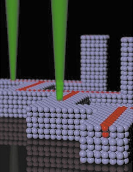
evaporates, and aided by convective and
    shear forces (such as from a stir bar), the
    spheres collect at the meniscus where
    capillary action causes them to slide up the
    substrate while self-assembling into a
    colloidal crystal film. Cracking at the
    silica necks is another problem, and this
    has been minimised by depositing further
    layers of silica on the spheres in situ using
    CVD (with silicon tetrachloride vapour
    undergoing acid-catalysed hydrolytic
    polycondensation); this additional process
    gives further control over connectivity and
    pore size.16,17
       The group has experimented with other
    structures and topologies, creating
    complex patterns comprising spheres of
    two different sizes – for example,
    hexagonally close-packed layers of large             Fig. 4 SEM images of the different steps in the MISO process (a) an inverse silica colloidal crystal
    spheres with a superimposed arrangement              micro-mould; (b) an inverse silica-silicon composite colloidal crystal; (c,d) a silicon colloidal crystal
    of much smaller spheres confined in the              with novel topology. Reproduced with permission from Adv. Mater. (ref. 19), copyright 2003 Wiley-
    interstices (Fig. 3).18 Ozin has also                VCH.
    developed a new photonic crystal topology
    by making an inverted silica opal (starting
    with a latex colloidal crystal) and coating        breakthrough in condensed matter physics.              using a laser attached to a scanning optical
    the air cavities with silicon using CVD.           But photonic crystals are of little use                microscope to perform laser microwriting
    Dissolving away the silica leaves behind a         unless, like semiconductors, you can                   and microannealing, a controlled
    3D structure made of spherical silicon             introduce defects, which modulate the                  crystalline phase change, and therefore
    shells interconnected by cylindrical               band structure, allowing light to be                   refractive index change, could be induced
    channels in an air background. Ozin dubs           manipulated. These include point or line               in defined regions of the crystal over a
    the technique MISO (micro-moulding in              vacancies at the length-scale of the                   range of length scales.20
    inverse silica opals) (Fig. 4). The different      photonic lattice constant, needed for                     The next step has been to make well-
    arrangement of necks between the spheres           waveguides or microlasers, and larger                  defined photonic crystal shapes on or
    means that the optical band properties are         defect architectures which can couple or               within a typical planar device like a silicon
    different but the opal structure still has a       switch light in specific regions of the                wafer, so as to create lasers, transistors,
    complete photonic bandgap.19                       photonic lattice. As a step in this direction,         waveguides and other microoptical devices
                                                       Ozin’s group has devised a method to                   that could be integrated in an all-optical
    Making a real device                               build patterns of refractive index contrast            chip. This was done by subtly combining
    These remarkable materials with their              (the defects) in a polycrystalline or                  soft lithography with colloidal crystal self-
    precise optical properties represent a major       amorphous silicon photonic crystal. By                 assembly. Ozin’s group fashioned V-
                                                                                                              shaped, rectangular and square channels in
                                                                                                              a silicon wafer and filled them with opal
                                                                                                              photonic crystals (Fig. 5).21 A line-
                                                                                                              patterned master of polydimethylsiloxane
                                                                                                              (PDMS) was inked with an alkanethiol in
                                                                                                              ethanol and printed onto a silicon wafer
                                                                                                              coated with gold and an adhesive layer of
                                                                                                              titanium. The exposed gold surface and the
                                                                                                              underlying silicon were sequentially
                                                                                                              etched away to form grooves. Silica
                                                                                                              microspheres dispersed in ethanol were
                                                                                                              then coaxed by capillary forces into the
                                                                                                              tunnels by directed evaporation-induced
                                                                                                              self-assembly or by placing a flat piece of
                                                                                                              PDMS over the grooves. As the ethanol
                                                                                                              evaporated, the microspheres collected
                                                                                                              into lines with the desired fcc crystal
                                                                                                              structure. Another approach that the team
                                                                                                              has worked on was to use spin-coating (the
                                                                                                              wafer is spun round while centrifugal
                                                                                                              forces spread the silica dispersion over it)
                                                                                                              to guide the spheres into sets of pre-
                                                                                                              formed channels or pits in the substrate.
                                                                                                              The pit dimensions can be designed so that
                                                                                                              they are commensurate with an integral
Fig. 3 Examples of binary colloidal crystal patterns and defects. Reproduced with permission from             number of spheres, resulting in well-
Adv. Mater. (ref. 18), copyright 2003 Wiley-VCH.                                                              defined ordering.22
                                                                                                                 A whole range of opal structures can be

                                This journal is © The Royal Society of Chemistry 2003                                            CHEM. COMMUN., 2003                 2641
based on dye-sensitised titanium dioxide
                                                                                                             can be improved by preparing the active
                                                                                                             material as an inverse opal microstructure.
                                                                                                                However, for the chemist, perhaps the
                                                                                                             most exciting possibilities arise from the
                                                                                                             colour-tunability presented by opal
                                                                                                             photonic crystals. “Chemists can now
                                                                                                             produce colours based on refractive index
                                                                                                             contrast rather than chromophores,” says
                                                                                                             Ozin. Since the diffraction colour depends
                                                                                                             on the photonic crystal lattice constant,
                                                                                                             changing the distance between the
                                                                                                             microspheres changes the colour. This can
                                                                                                             be achieved by filling the interstitial
                                                                                                             spaces of the colloidal crystal with a
                                                                                                             polymer gel that swells or shrinks in
                                                                                                             response to an external effect. The process
                                                                                                             could be used in a sensor or even to make
                                                                                                             a photonic ink (P-Ink).26 In the latter, the
                                                                                                             distance between the unattached spheres is
                                                                                                             determined by a redox-active
                                                                                                             metallopolymer gel (partially cross-linked
                                                                                                             polyferrocenylsilane). The redox state of
                                                                                                             the iron atoms, which can be controlled
                                                                                                             electrochemically, reversibly changes the
                                                                                                             amount of solvent the polymer absorbs, on
                                                                                                             a sub-second switching time.
                                                                                                                It’s interesting to note the many
                                                                                                             directions in which the original work,
         Fig. 5 (a) Opal crystals forming inside rectangular-shaped microchannels on a flat substrate;       based on specific physics, has taken
         (b) an SEM of the structures that form. Reproduced with permission from Adv. Funct. Mater.          someone with a background in inorganic
         (ref. 21), copyright 2002 Wiley-VCH.                                                                and materials chemistry. Ozin hopes that
                                                                                                             other chemists will be stimulated to look at

       made in this way using various surface
       relief patterns, including free-standing
       microfibres (Fig. 6)23 and heterostructures
       consisting of two sizes of spheres suitable
       as optical filters and mirrors. There’s also
       the potential to introduce other active
       molecules such as liquid crystals and
       luminescent guests, or to use other
       materials. An all-optical transistor could,
       for example, be based on the large
       refractive-index change accompanying the
       metal-to-nonmetal transition induced in an
       inverse colloidal crystal of vanadium
       dioxide by a femtosecond laser. A serious
       problem still to be overcome is how to get
       light in and out of a photonic crystal and
       with minimal light scattering losses. One
       approach Ozin is working on is to create
       connecting structures with a refractive
       index gradient using the laser writing
       technique.

       Other applications of opal
       technology
       Although the opal approach to optical
       circuits and computers is promising, Ozin
       admits that it may not be the final answer.
       However, he is convinced that the
       underlying chemical methodology, based
       on 50 years of colloid chemistry, has great
       potential in many other areas, from battery
       materials to visual displays. It has already         Fig. 6 SEMs of silicon–silica composite and inverted silicon colloidal crystal fibres at different
       been shown that the efficiency of tin                magnifications. Reproduced with permission from Adv. Mater. (ref. 23), copyright 2002 Wiley-VCH.
       dioxide gas sensors24 and solar cells25

2642   CHEM. COMMUN., 2003                                       This journal is © The Royal Society of Chemistry 2003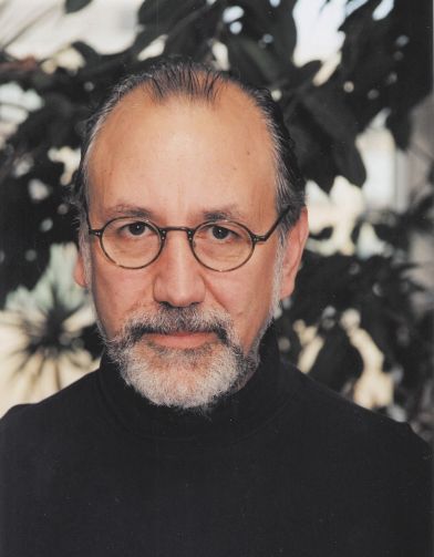
this novel approach to chemical                      2059.                                              J. Norris, Nature (London), 2001, 414,
manipulation, whereby chemical form and            5 S. John, Phys. Rev. Lett., 1987, 58, 2486.         289.
physical function are so happily married at        6 E. Yablonovitch, Sci. Am., December 2001,     17   H. Míguez, N. Tétreault, B. Hatton, S. M.
the nano and mesoscopic level.                       35.                                                Yang, D. Perovic and G. A. Ozin, Chem.
                                                   7 P. Russell, Science (Washington D.C.),             Commun., 2002, 2736.
                                                     2003, 299, 358.                               18   V. Kitaev and G. A. Ozin, Adv. Mater.,
Acknowledgements                                   8 B. T. Holland, C. Blanford and A. Stein,           2003, 15, 75.
                                                     Science (Washington D.C.), 1998, 281,         19   H. Míguez, N. Tétreault, S. M. Yang, V.
Nina Hall thanks Professor Ozin for his
                                                     538.                                               Kitaev and G. A. Ozin, Adv. Mater., 2003,
help with this article, and his coworkers,
                                                   9 J. E. G. J. Wijnhoven and W. L. Vos,               15, 597.
André Arsenault, Vladimir Kitaev, Hernán             Science (Washington D.C.), 1998, 281,         20   N. Tétreault, H. Míguez, V. Kitaev, S. M.
Míguez, Nicolas Tétreault and San Ming               802.                                               Yang and G. A. Ozin, Adv. Mater., 2003,
Yang. Professor Ozin acknowledges the             10 A. A. Zakhidov, R. H. Baughmann, Z.                15, 1167.
financial support for this work from the             Iqbal, C. Cui, I. Khayrullin, S. O. Dantas,   21   S. M. Yang, H. Míguez and G. A. Ozin,
Natural Sciences and Engineering                     J. Marti and V. G. Ralchenko, Science              Adv. Funct. Mater., 2002, 12, 425.
Research Council of Canada as well as the            (Washington D.C.), 1998, 282, 897.            22   G. A. Ozin and S. M. Yang, Adv. Funct.
University of Toronto.                            11 R. C. Salvarezza, L. Vázquez, H. Míguez,           Mater., 2001, 11, 95.
                                                     R. Mayoral, C. López and F. Meseguer,         23   H. Mignez, S. M. Yang, N. Tetreault and
                                                     Phys. Rev. Lett., 1996, 77, 4572.                  G. A. Ozin, Adv. Mater., 2002, 14, 1805.
Notes and references                              12 H. Míguez, C. López, F. Meseguer, A.          24   R. W. J. Scott, S. M. Yang, N. Coombs, G.
 1 J. D. Joannopoulos, P. R. Villeneuve and S.       Blanco, L. Vázquez, R. Mayoral, M.                 A. Ozin and D. E. Williams, Adv. Mater,
   Fan, Nature (London), 1997, 386, 143.             Ocaña, V. Fornés and A. Mifsud, Appl.              2001, 13, 1468.
 2 A. Blanco, E. Chomski, S. Grabtchak, M.           Phys. Lett., 1997, 71, 1148.                  25   S. Nishimura, N. Abrams, B. A. Lewis, L.
   Ibisate, S. John, S. W. Leonard, C. Lopez,     13 H. Míguez, F. Meseguer, C. López, A.               I. Halaoui, T. E. Mallouk, K. D.
   F. Meseguer, H. Míguez, J. P. Mondia, G.          Blanco, J. S. Moya, J. Requena, A. Mifsud          Bekenstein, J. van de Lagemaat and A. J.
   A. Ozin, O. Toader and H. M. van Driel,           and V. Fornés, Adv. Mater., 1998, 10, 483.         Frank, J. Am. Chem. Soc., 2003, 125,
   Nature (London), 2000, 405, 437.               14 P. Jiang, J. F. Bertone, K. S. Hwang and V.        6306.
 3 S. Y. Lin and J. G. Fleming, IEEE J.              L. Colvin, Chem. Mater., 1999, 11, 2132.      26   A. C. Arsenault, H. Míguez, V. Kitaev, G.
   Lightwave Technol., 1999, 17, 1944.            15 V. L. Colvin, MRS Bull., 2001, 26, 637.            A. Ozin and I. Manners, Adv. Mater., 2003,
 4 E. Yablonovitch, Phys. Rev. Lett., 1987, 58,   16 Y. A. Vlasov, X.-Z. Bo, J. C. Sturm and D.         15, 503.

                           This journal is © The Royal Society of Chemistry 2003                                     CHEM. COMMUN., 2003             2643
You can also read