The Study on Al xGa1-xN Film Deposition by Radio Frequency Magnetron Sputtering - IOPscience
←
→
Page content transcription
If your browser does not render page correctly, please read the page content below

Journal of Physics: Conference Series

PAPER • OPEN ACCESS

The Study on AlxGa1-xN Film Deposition by Radio Frequency Magnetron
Sputtering
To cite this article: Danxia Deng et al 2021 J. Phys.: Conf. Ser. 1885 052022

View the article online for updates and enhancements.

                               This content was downloaded from IP address 46.4.80.155 on 23/05/2021 at 08:28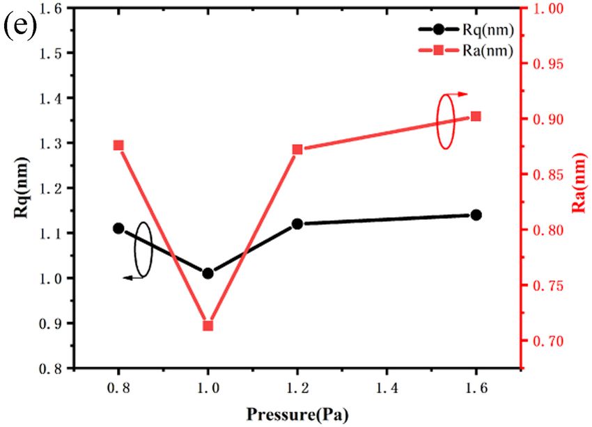
ICAMMT 2021                                                                                                     IOP Publishing
Journal of Physics: Conference Series                         1885 (2021) 052022          doi:10.1088/1742-6596/1885/5/052022

The Study on AlxGa1-xN Film Deposition by Radio Frequency
Magnetron Sputtering

                     Danxia Denga, Zuoyan Qinb, Hao Huc, Lei Jind, Zhenhua Sune and Honglei Wuf,*
                     Key Laboratory of Optoelectronic Devices and Systems of Ministry of Education and
                     Guangdong Province, College of Physics and Optoelectronic Engineering, Shenzhen
                     University, Shenzhen, Guangdong, China
                     a
                      email:1800282005@email.szu.edu.cn, bemail: 2176285305@email.szu.edu.cn, cemail:
                     1810285013@email.szu.edu.cn, djinlei851024@126.com, eemail: szh@szu.edu.cn
                     *Correspondence: femail: hlwu@szu.edu.cn; Tel: +86-7552-653-8557

                     Abstract:A series of AlxGa1-xN films are deposited on Si (111) substrates by radio frequency
                     magnetron sputter with different experimental Parameters. Crystallinities, elemental
                     components and surface morphologies of films are investigated in terms of their deposition
                     Parameters. The results reveal that the films grow along with the (004) crystal direction and
                     have a more Al component than the target, which is attributed to the higher bond energy of
                     Al-N. A higher pressure and nitrogen concentration lead to more surface structures such as
                     bubbles on the AlxGa1-xN films. Using a pressure of 1.0 Pa and nitrogen concentration of 33%,
                     AlxGa1-xN films with good quality are finalized achieved.

1. Introduction
III-V group nitride semiconductors (GaN, A1N, BN, InN) and their alloys have great application
potential in electronic and optoelectronic devices. In Particular,AlxGa1-xN, which is the alloy of GaN
and AlN, has become one research hot spot in recent years.AlxGa1-xN has a tunable direct bandgap
which varies with Al composition from 3.4 eV (GaN) to 6.2 eV (AlN).This feature makes AlxGa1-xN
good candidate of emission materials in ultraviolet emitting devices covering UV-A (400nm-320nm),
UV-B (320nm-280nm),and UV-C (280nm-200nm)[1][2][3].Alternatively,AlxGa1-xN can be used for solar
blind ultraviolet detectors due to its proper bandgap, which corresponds to wavelength from 365nm to
200nm[4][5][6].Furthermore,AlxGa1-xN has good electrical properties including high breakdown field
strength and saturation electron drift velocity, leading to outstanding application performance in
semiconductor power devices [7][8] and high speed transistors[9][10].Finally, the high quality AlxGa1-xN
material can also be used as substrates for the growth of III-V group semiconductors .
    To obtain high quality AlxGa1-xN films, metal organic chemical vapor deposition (MOCVD)[11][12],
molecular beam epitaxy (MBE)[13][14] and pulsed laser deposition (PLD)[15][16] are the mostly used
technologies. Nevertheless, these technologies are expensive, dangerous, and low yield. They are
suitable for very thin film growth aiming at scientific research in laboratory instead of massive
production. In this regard, magnetron sputtering is a promising alternative technology for the growth
of AlxGa1-xN. However,while AlN[17][18]and GaN[19][20] semiconductor films with good quality have
been grown successfully using magnetron sputtering, there is less reports of using this technology to
grow AlxGa1-xN at present. This work tries to fill this gap between AlxGa1-xN growth and magnetron

              Content from this work may be used under the terms of the Creative Commons Attribution 3.0 licence. Any further distribution
              of this work must maintain attribution to the author(s) and the title of the work, journal citation and DOI.
Published under licence by IOP Publishing Ltd                          1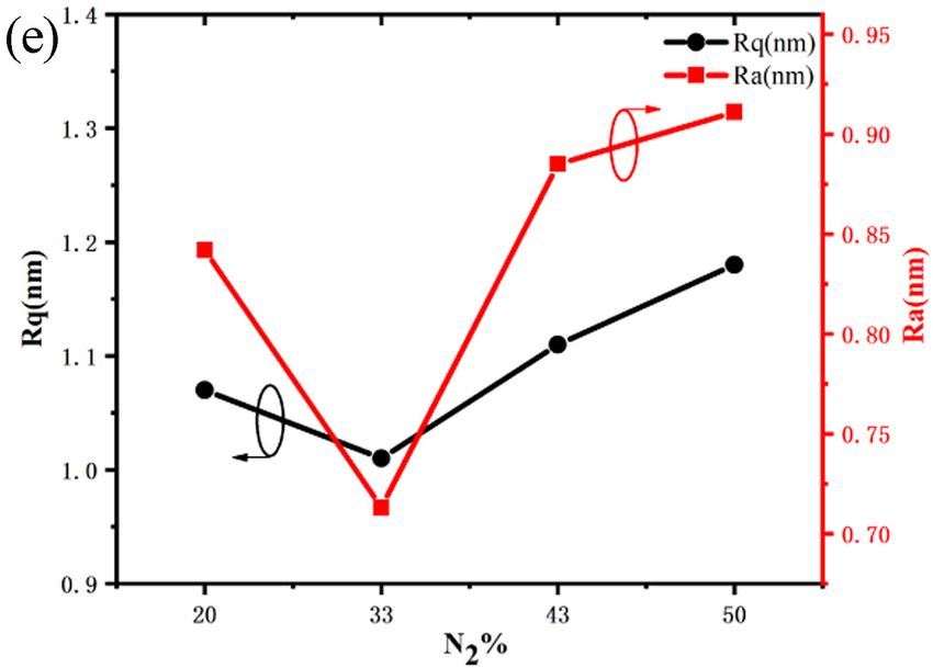
ICAMMT 2021                                                                                IOP Publishing
Journal of Physics: Conference Series          1885 (2021) 052022    doi:10.1088/1742-6596/1885/5/052022

sputtering by studying the growth condition of AlxGa1-xN films using radio frequency (RF) magnetron
sputter equipment.

2. Experimental
AlxGa1-xN films were deposited on Si (111) wafers using RF magnetron sputtering. The substrates
were ultrasonically cleaned with acetone, ethanol, and deionized water to remove surface stains, and
then treated by O2 plasma in plasma cleaner. A Al0.6Ga0.4N target with 99.99% purity was used for the
sputtering in Argon (Ar) and Nitrogen (N2) mixed atmosphere. The RF power was fixed to be 45W.
Prior to deposition, the chamber was evacuated to a pressure of 5×10⁻⁴ Pa. The target was cleaned by
Ar+ bombardment for 10 mins. The deposition was block by a shutter above the substrate until the
sputtering rate was stabilized. The growth time was set to be 3 hours. Based on the above recipe, the
AlxGa1-xN film deposition was conducted with either variable pressure or N2 concentration, producing
two groups of samples. For the first group, the N2 concentration was set to be 33 %(volume
ratio) ,while the total pressure in the chamber varied from 0.8 Pa to 1.6 Pa. The second group was
about N2 concentrations, which was adjusted across the desired condition. The deposition process is
illustrated in Fig.1.
    The crystalline structure was characterized using X-ray diffractmeter (XRD, Rigaku Ultima IV).
The surface morphology and the cross section of the films were observed by scanning electron
microscope (SEM,SU3500).The elemental compositions of samples were detected using
Energy-dispersive X-ray spectroscope (EDS,JSM-5910LV). The atomic force microscope (AFM,
Bruker) was used to determine surface roughness of films.

                      Fig.1 Schematic of the deposition process of AlxGa1-xN films.

3. Results and discussion

3.1 Influence of sputtering pressure on the texture of AlxGa1-xN films

                Fig.2 XRD spectra of AlxGa1-xN films with different sputtering pressure.

                                                     2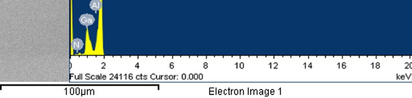
ICAMMT 2021                                                                               IOP Publishing
Journal of Physics: Conference Series          1885 (2021) 052022   doi:10.1088/1742-6596/1885/5/052022

Fig.2 shows the XRD spectra of AlxGa1-xN films deposited at a sputtering power of 45W and 33% N2
with sputtering pressure of 0.8 Pa, 1.0 Pa, 1.2 Pa, and1.6 Pa. According to PDF#25-1133 and
#50-0792 diffraction cards, the 2θ of AlN (004) and GaN (004) are 76.4°and 72.9°, respectively. We
can infer that the diffraction peak of 75.7° on the graph is AlxGa1-xN (004). Only (004) peak can be
found the measured range, indicating that the film was grown with the (004) plane Parallel with the
substrate. Fig. 2 shows that the pressure is 1.0 Pa, which has the highest diffraction peak. With the
pressure increasing, the mean free Path of the sputtered Particles was shortened in the chamber. The
sputtered Particles would experience more gas scattering before arriving at the substrate surface with
most of their kinetic energy dissipated. Hence, it is difficult to rearrange the atoms on the substrates.

                         Fig.3 The EDS results of AlxGa1-X film grown at 1.0 Pa.

    The EDS spectrum of the film grown at 1.0 Pa is showed in Fig.3. The EDS results of all four film
shows the existence of Al, Ga and N elements, confirming the AlxGa1-xN composition. The atom ratio
of Al to Ga of the sample of 0.1 Pa is 3:1. This value of the target is is 3:2. The high Al concentration
in the film can be ascribed to that Al atoms are easier to combine with N than Ga since The Al-N bond
energy is 2.88 eV, and Ga-N bond energy is 2.2 eV.During the film deposition, Al atoms are more
competitive than Ga atoms, resulting in an increase in Al composition in the AlxGa1-XN films.

          Fig.4 SEM image for AlxGa1-xN films of (a) 0.8 Pa, (b) 1.0 Pa, (c)1.2 Pa, (d) 1.6 Pa.

                                                    3
ICAMMT 2021                                                                                IOP Publishing
Journal of Physics: Conference Series          1885 (2021) 052022    doi:10.1088/1742-6596/1885/5/052022

    SEM images of AlxGa1-xN thin films grown at various pressures are shown in Fig.4. Increasing
pressure from 0.8 to 1.0 Pa results in the decreasing of defects. Further increase of the pressure
induces defects on the surface of the samples. The defects appear as bubbles and become larger as the
pressure increases. The cause of the defects can be explained considering the growth mechanism. The
sputtered Al, Ga and N atoms from target converge on substrate surface. At the early stage of growth,
these atoms will first form a cluster. After that, more atoms will gather around the cluster and then
crystalize based on the cluster sequentially. If the sputtering pressure is too high, for example, 1.6 Pa,
the atoms that reach the substrate will not have enough energy to rearrange, and thus forming defects
in the films. In addition, there is a large lattice mismatch and thermal mismatch between the Si (111)
and the AlxGa1-xN films. With the growth time prolonged, these defects will be further amplified. From
the results of SEM, the optimum growth pressure is 1.0 Pa, which produced no obvious bubbles on the
film surface.

 Fig.5 AFM images(10µm×10µm) of AlxGa1-xN films of (a) 0.8 Pa,(b)1.0 Pa,(c) 1.2 Pa (d) 1.6 Pa; (e):
           Rq and Ra along with pressures. The data are extracted from the AFM images.

                                                     4
ICAMMT 2021 IOP Publishing
Journal of Physics: Conference Series 1885 (2021) 052022 doi:10.1088/1742-6596/1885/5/052022
The 3D AFM images (10µm×10µm) of the films grown under different pressure are shown in Fig 5.
In general, the values of the Rq (root mean square of roughness) and Ra(average roughness) increase as
the pressure increases. At 1.0 Pa, the roughness of the AlxGa1-xN film is the lowest, with Rq=1.01 nm
and Ra=0.71 nm. So, the best sputtering pressure can be nailed down to be 1.0 Pa, which is consistent
with SEM analysis.
3.2 Influence of growth atmosphere on the texture of AlxGa1-xN films
Fig.6 XRD spectra of AlxGa1-xN films grown in atmospheres with N2 proportions.
Fig.6 shows the XRD Patterns of AlxGa1-xN films deposited in atmospheres with different N2
proportions with a sputtering pressure of 1.0 Pa and a fixed power of 45W. All the samples were found
to have AlxGa1-xN (004) in the measured range except for the diffraction peak from the Si substrate.
The (004) peak for 33% N2 has the most strong intensity. The reason is that since the sputtering
pressure is constant, increasing N2 proportion means reducing the Ar+.And reducing the Ar+ will
directly decrease the sputtering yield of the target. So, an atmosphere of lower N2 proportion means
that the Al and Ga Particles are of higher kinetic energies to transfer to the substrate for crystallization.
If the nitrogen concentration is lower, firstly, enough N atoms cannot be supplied into the chamber.
Secondly, during the experiments, it was found that when the nitrogen concentration is too low, Ar+
will carry more energy. Although this energy cannot cause the target to crack, the surface of the target
becomes black.
5ICAMMT 2021 IOP Publishing
Journal of Physics: Conference Series 1885 (2021) 052022 doi:10.1088/1742-6596/1885/5/052022
Fig.7 SEM image of AlxGa1-xN films grown in atmospheres with N2 proportions of (a)20%, (b) 33%,
(c )43%, (d) 50%.
N2 proportion in atmosphere is a key factor affecting film quality. The surface morphology of the
films grown in atmospheres with N2 proportions of 20%, 33%, 43%, and 50%are shown in the Fig.7.
With high N2 proportion of 43% and 50%, lots of bubbles appear on the surface of the samples. In
contrast, the AlxGa1-xN film of 33% N2 proportion does not have obvious defects. We speculate that
high nitrogen concentration would lead to the reduction of ionized Ar+. Therefore, the energy
bombarding the target is reduced, and the energy of the sputtered target atoms is reduced. Insufficient
atomic energy would lead to defects. Hence, the optimal N2 proportion should be around 33 %.
6ICAMMT 2021 IOP Publishing
Journal of Physics: Conference Series 1885 (2021) 052022 doi:10.1088/1742-6596/1885/5/052022
Fig.8 AFM images (10µm×10µm) of AlxGa1-xN films grown in atmospheres with N2 proportions of
(a)20%, (b) 33%, (c )43%, (d) 50%; (e): Rq and Ra along with the N2 proportions. The data are
extracted from the AFM images.
Fig. 8 is the AFM characteristics of AlxGa1-xN films grown in different atmospheres. The Rq and Ra
of the film of 33% N2 proportion is smallest, indicating for a consistent conclusion with the SEM
analysis, that is, the atmosphere with 33% N2 proportion is the best growth condition for AlxGa1-xN
film.
Fig.9 The cross-section SEM image of the AlxGa1-xN film grown in atmosphere with N2 proportion of
33%.
The cross-section SEM image of the AlxGa1-xN film grown in atmosphere with N2 proportion of
33% is shown in Fig.9. The film thickness was measured to be ~250 nm. It is worth of noting that to
attain this thickness, the growth lasted three hours. The deposition speed is expected to be increased by
increase the sputtering power, which would bring about the demand of high-quality target that can
sustain under a high power.
4. Conclusions
In summary, RF magnetron sputtering technique was used to deposit AlxGa1-xN films. The XRD
results showed the films grew with a [004] orientation. The EDS results revealed the higher Al content
7ICAMMT 2021 IOP Publishing
Journal of Physics: Conference Series 1885 (2021) 052022 doi:10.1088/1742-6596/1885/5/052022
in the film than the target, which was ascribed to that the higher Al-N bond energy than Ga-N induced
a preferred Al integration. The influences of sputtering pressure and N2 proportion in the atmosphere
on the film quality were investigated for an optimized growth condition. It was raveled that both high
sputtering pressure and high N2 proportion in the atmosphere would deteriorate the quality of the
AlxGa1-xN films. The best Parameters were ascertained, which are the sputtering pressure of 1.0 Pa and
N2 proportion of 33% in the atmosphere At the end of the article, it is proposed to improve the quality
of the target to improve the deposition speed. These explorations can provide a reference for the
development of magnetron sputtering deposition technique of high quality AlxGa1-xN films.
Acknowledgments
The authors gratefully acknowledge the financial support from the National Natural Science
Foundation of China (Grant No. 61974094), the Key Research and Development Project of
Guangdong Province (Grant No. 2020B010169003) and the Science and Technology Innovation
Commission of Shenzhen (Grant No.JCYJ20200109105413475).
References
[1]Parbrook,P.,Wang,T.(2011)Light Emitting and Laser Diodes in the Ultraviolet. IEEE.J.Sel.Top.
Quant.,17:1402-1411.
[2]Yasan,A.,McClintock,R.,Mayes,K.,etal.(2003)4.5mW operation of AlxGa1-xN-based 267nm
deep-ultraviolet light-emitting diodes.Appl.Phys.Lett.,83:4701-4703.
[3]Lochner,Z.,Kao,T.T.,Liu,Y.S.,etal.(2013)Deep-ultraviolet lasing at 243 nm from photo-pumped
AlxGa1-xN/AlN heterostructure on AlN substrate.Appl.Phys.Lett.,102:101110.
[4]Sang,L.W.,Qin,Z.X.,Cen,L.B.,etal.(2008)AlxGa1-xN-Based Solar-Blind Schottky Photodetectors
Fabricated on AlN/Sapphire Template.Chinese.Phys.Lett.,25:258-261.
[5]Rehm,R.,Driad,R.,Kirste,L.,etal.(2020)Toward AlxGa1-xN Focal Plane Arrays for Solar-Blind
Ultraviolet Detection.Phys.Status.Solidi.A.,217:1900769.
[6]Kalra,A.,Rathkanthiwar,S.,Muralidharan,R.,etal.(2020)Material-to-device performance correlation
for AlxGa1-xN-based solar-blind p–i–n photodiodes.Semicond.Sci.Technol.,35:035001.
[7]ShepPard,S.T.,Doverspike,K.,Pribble,W.L.,etal.(1999)High-Power Microwave GaN/AlxGa1-xN
HEMT’s on Semi-Insulating Silicon Carbide Substrates. IEEE.Electr.Device.L., 20:161-163.
[8]Hao,X.,Choong,H.L.,Kamal,H.,etal.(2019)Al0.75Ga0.25N/Al0.6Ga0.4N heterojunction field effect
transistor with fT of 40 GHz. Appl. Phys. Express.,12: 066502.
[9]Kumar,V.,Kuliev,A.,Schwindt.R.,etal.(2003)High performance 0.25um gate-length
AlxGa1-xN/GaN HEMTs on sapphire with power density of over 4.5 W/mm at 20 GHz.
Solid-State Electronics.,47:1577-1580.
[10]Tokuda,H.,Yamazaki,J.,Kuzuhara.M.(2010)High temperature electron transport properties in
AlxGa1-xN/GaN heterostructures.J APPL PHYS.,108:104509.
[11]Huang,G.S.,Yaoh.H.H.,Kuo,H.C.etal.(2007)Effect of growth conditions on the Al composition and
quality of AlxGa1-xN film.Mater.Sci.Eng.B.,136: 29-32.
[12]Chen,H.,Zhang,X.,Chen,S.,etal.(2020)Properties of Si-doped a-plane AlxGa1-xN layers. Mat.Sci.
Semicon.Proc.,119:105270.
[13]Mizerovn,A.M.,Jmerik,V.N.,Yagovkina,M.A.,etal.(2011)Role of strain in growth kinetics of
AlxGa1-xN layers during plasma-assisted molecular beam epitaxy.J.Cryst.Growth., 323:68-71.
[14]Hentschel,R.,Gärtner,J.,Wachowiak,A.,etal.(2018)Surface morphology of AlxGa1-xN/GaN
heterostructures grown on bulk GaN by MBE.J.Cryst.Growth.,500:1-4.
[15]Huanga,T.F.,Harris,J.S.(1998)Growth of epitaxial AlxGa1-xN films by pulsed laser deposition.
Appl.Phys.Lett.,72:1158-1160.
[16]Masuyama,Y.,Komatsu,S.,Kiso,M.,etal.(2003)Effect of Ga Re-evaporation on AlxGa1-xN Thin
Film Growth by Dual-Beam Pulsed Laser Deposition Method in N2 Ambient.Jpn.J.
Appl.Phys.,42:2856-2857.
8ICAMMT 2021 IOP Publishing
Journal of Physics: Conference Series 1885 (2021) 052022 doi:10.1088/1742-6596/1885/5/052022
[17]Cheng,H.,Sun,Y.,Zhang,J.X.,etal.(2003)AlN films deposited under various nitrogen concentrations
by RF reactive sputtering.J.Cryst.Growth.,254:46-54.
[18]Mogami,Y.,Motegi,S.,Osawa,A.,etal.(2019)Evolution of morphology and crystalline quality of
DC-sputtered AlN films with high-temperature annealing.Jpn.J.Appl.Phys.,58:SC1029.
[19]Yin,M.L.,Zou,C.W.,Li,M.,etal.(2007)Middle-frequency magnetron sputtering for GaN growth.
Nuclear Instruments and Methods in Physics Research B.,262:189–193.
[20]Mantarci,A.,Kundakci,M.(2019)Power-dependent physical properties of GaN thin films deposited
on sapphire substrates by RF magnetron sputtering.Bull.Mater.Sci., 42:196.
9You can also read