Tip-Enhanced Raman Scattering - Nt-MDT
←
→
Page content transcription
If your browser does not render page correctly, please read the page content below
Scientific Digest
Tip-Enhanced Raman Scattering
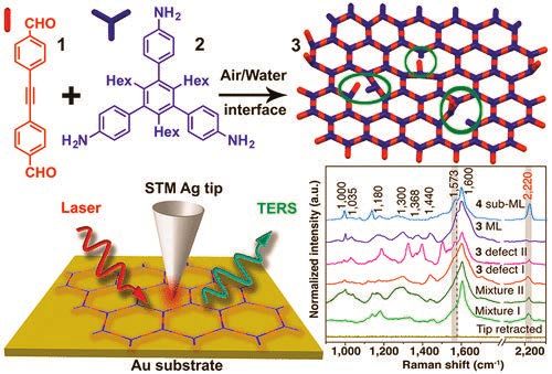
Tip-Enhanced Raman Scattering (TERS, nano-Raman) is the technique for
enhancement of weak Raman signals and for super-resolution Raman imaging
with spatial resolution ~10 nm. Nano-Raman imaging provides unique insights into
sample structure and chemical composition on the nanometer scale.
In TERS, a sharp metal probe (nano-antenna) is used to localize and enhance optical
field at the tip apex. The light enhancement is typically appeared when excitation laser
light is in resonance with localized surface plasmon at the end of the TERS probe.
Enhancement of electromagnetic field (light) intensity on the TERS probe apex can
reach many orders of magnitudes. In TERS mapping the sample is scanned with
respect to the nano-antenna. Therefore the enhanced Raman signal localized near
the probe apex approached to the sample resulting in Raman map of the sample
surface with nanometer scale resolution.
www.ntmdt-si.com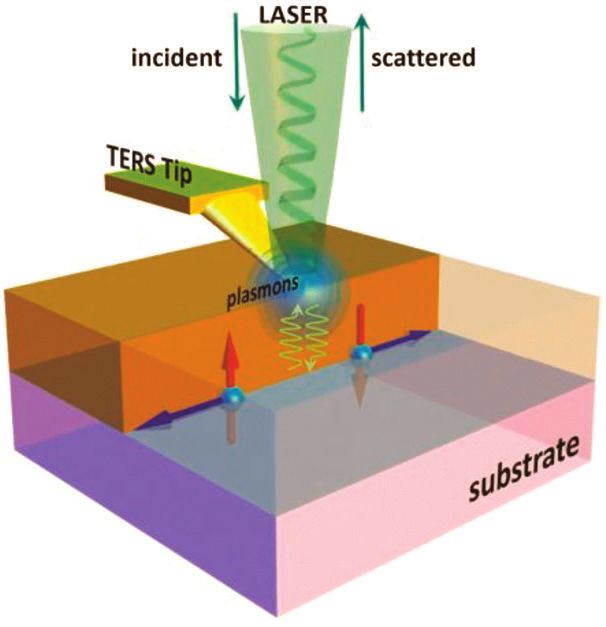
Scientific Digest

                        Development of a Candidate Reference Sample for the
                        Characterization of Tip-Enhanced Raman Spectroscopy
                        Spatial Resolution
                        Alessio Sacco, Dario Imbraguglio, Andrea M. Giovannozzi, Chiara Portesi and Andrea
                        M. Rossi
                        RSC Advances 2018, 8, 27863-27869
                        http://xlink.rsc.org/?DOI=c8ra03762k

Tip-Enhanced Raman Spectroscopy (TERS) is a topographic
and chemical analysis technique with nanoscale resolution,
consisting of the combination of Scanning Probe Microscopy
(SPM) and Localized Surface Plasmon Resonance (LSPR) for
the enhancement of Raman scattering in the vicinity of the probe.
The quantification of spatial resolution represents an important
issue, and, as of now, standards for calibration are not available.
In the present work a candidate reference sample for TERS
measurements was fabricated. It consists of a flat, conductive
gold surface with a nanometric grating of a self-assembled
monolayer of Raman-active organic molecules fabricated by an
optimized Electron Beam Lithography (EBL) method to replicate
established SPM calibration standards. Its feasibility as a TERS
standard was tested by STM-TERS imaging.

                        Spectrally Resolving Coherent TERS Spectroscopy of
                        Electrically Biased Carbon-Coated Fibers

                        Sergey S. Kharintsev, Svetlana V. Saparina, Alexandr I. Fishman, Andrei A. Stolov, and
                        Jie Li
                        J. Phys. Chem. C 2020, 124, 27, 14752–14758
                        https://doi.org/10.1021/acs.jpcc.0c05228

Tip-Enhanced Raman Scattering (TERS) represents an
advanced spectroscopic tool that enables probing a specimen
on scales far beyond the diffraction limit. An investigation of two-
dimensional systems reveals a striking feature of TERS, when the
near-field intensity is governed by the 8th and 10th power
of the tip–sample distance for the coherent and incoherent
scattering cases, respectively. We demonstrate spectrally
resolving capabilities of coherent TERS spectroscopy when
studying electrically biased amorphous carbon films. Local
electro-annealing at hot spots was found to activate
temperature-dependent      molecular       transformations     such
as an expansion of the defect-free sp2 domains network at
temperatures above 400 °C. Electro-assisted TERS allows
one to directly visualize the presence of water-decorated
carboxyl/hydroxyl groups at the edge carbon atoms.

                                                          2
Tip-Enhanced Raman Scattering

                         Novel Approaches in Tip-Enhanced Raman Spectroscopy:
                         Accurate Measurement of Enhancement Factors and
                         Pesticide Detection in Tip Dimer Configuration
                         Sacco, A., Mangino, S., Portesi, C., Vittone, E., & Rossi, A. M.
                         Journal of Physical Chemistry C, 2019, 123(40), 24723–24730
                         https://doi.org/10.1021/acs.jpcc.9b07016

Tip-Enhanced Raman Spectroscopy (TERS) allows the precise
manipulation of a nanometric probe for surface chemical analysis
by plasmon-based amplification of Raman signals; however,
acknowledged procedures and materials for assessing the
enhancement factor in different configurations are still lacking. In
this work, we propose a technique for the standardization of TERS
intensity measurements, by chemisorption of different organic
Raman-active molecules on plasmonic probes, and compare it
to the conventional procedures addressed to the same goals.
In addition, by ideally considering TERS as a special case of
surface-enhanced Raman (SERS) involving a single nanoparticle,
it was experimentally realized the three most common
configurations in SERS: isolated particle, single scattering probe
on a surface, and nanoparticle dimers.

                         Probing the Edge-related Properties of Atomically
                         thin MoS2 at Nanoscale

                         Huang, T. X., Cong, X., Wu, S. S., Lin, K. Q., Yao, X., He, Y. H., Wu, J. Bin, Bao, Y. F.,
                         Huang, S. C., Wang, X., Tan, P. H., & Ren, B.
                         Nature Communications, 2019, 10(1), 4–11
                         https://doi.org/10.1038/s41467-019-13486-7

Defects can induce drastic changes of the electronic properties of
two-dimensional transition metal dichalcogenides and influence
their applications. It is still a great challenge to characterize small
defects and correlate their structures with properties. Here, we
show that Tip-Enhanced Raman Spectroscopy (TERS) can obtain
distinctly different Raman features of edge defects in atomically
thin MoS2, which allows us to probe their unique electronic
properties and identify defect types (e.g., armchair and zigzag
edges) in ambient. We observed an edge-induced Raman peak
(396 cm−1) activated by the double resonance Raman scattering
process and revealed electron–phonon interaction in edges. The
power of TERS demonstrated in MoS2 can also be extended to
other 2D materials, which may guide the defect engineering for
desired properties.

                                                            3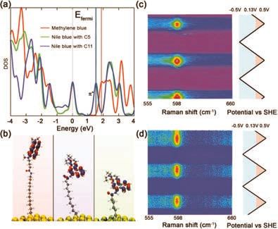
Scientific Digest
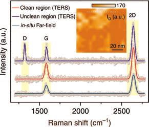
Towards Super-Сlean Graphene
Lin, L., Zhang, J., Su, H., Li, J., Sun, L., Wang, Z., Xu, F., Liu, C., Lopatin, S., Zhu, Y.,
Jia, K., Chen, S., Rui, D., Sun, J., Xue, R., Gao, P., Kang, N., Han, Y., Xu, H. Q., Liu, Z.
Nature Communications, 2019, 10(1), 1–7
https://doi.org/10.1038/s41467-019-09565-4
Among the various methods for graphene synthesis, chemical
vapour deposition (CVD) approach holds great potentials in the
scalable and cost-efficient production in a controllable fashion.
Typically CVD graphene consist of unavoidable contamination
on the surface during the growth process. Confocal micro Raman
does not allow identify defect regions as amount of defects is
not so large. Thanks to local enhancement and few nm lateral
resolution by TERS technique one can clearly identify regions
with defects (bright color on the map) and without (dark color on
the map). It is possible due to strong D-band in the TERS spectra
(upper spectrum) produced by defects. On the image there are
TERS spectra of the unclean (blue line) and clean (red line)
graphene regions in unclean graphene sample with Lorentzian
line fit analysis, and in-situ far-field Raman spectrum of graphene
in the same region (dark cyan line).
Superresolution Stimulated Raman Scattering Microscopy
Using 2-ENZ Nano-Composites
Kharintsev, S. S., Kharitonov, A. V., Alekseev, A. M., & Kazarian, S. G.
Nanoscale, 2019, 11(16), 7710–7719
https://doi.org/10.1039/c8nr09890e
Superlensing plays a crucial role in near- and far-field optical
imaging with sub-wavelength resolution. One of the ways to
expand optical bandwidth is surface plasmon resonances in
layered metal-dielectric nanostructures. These resonances are
commonly excited at a tunable single frequency. In this study,
we propose the concept of a multimode far-field superlens made
of a titanium oxynitride (TiON) thin film, that is a disordered
metal-dielectric refractory nano-composite. These films exhibit a achieved due to both the enhanced
double epsilon-near-zero (2-ENZ) behavior near the percolation third-order optical nonlinearity and the
threshold and, therefore, favor super-coupling the incident laser multiplicative nature of four-wave mixing.
light to surface plasmon resonances, not using such couplers as The multimode tunable far-field superlens
a prism, a grating, etc. We experimentally observe stimulated will impact emerging diffraction-free
Raman gain emission from nano-structured TiON thin films far-field optical microscopy, random
exposed to low-power continuous-wave laser light. It is shown Raman lasing on meta-atoms and
that superresolution of
Tip-Enhanced Raman Scattering

                         The Effect of Substrate and Surface Plasmons on Symmetry
                         Breaking at the Substrate Interface of the Topological
                         Insulator Bi2Te3
                         Wiesner, M., Roberts, R. H., Lin, J. F., Akinwande, D., Hesjedal, T., Duffy, L. B., Wang,
                         S., Song, Y., Jenczyk, J., Jurga, S., & Mroz, B.
                         Scientific Reports, 2019, 9, 6147
                         https://doi.org/10.1038/s41598-019-42598-9

A pressing challenge in engineering devices with topological
insulators (TIs) is that electron transport is dominated by the bulk
conductance, and so dissipationless surface states account for
only a small fraction of the conductance. Enhancing the surface-
to-volume ratio is a common method to enhance the relative
contribution of such states. In thin films with reduced thickness,
the confinement results in symmetry-breaking and is critical for
the experimental observation of topologically protected surface
states. We employ micro-Raman and Tip-Enhanced Raman
Spectroscopy to examine three different mechanisms of symmetry
breaking in Bi2Te3 TI thin films: surface plasmon generation,
charge transfer, and application of a periodic strain potential. We         a good agreement with previous theoretical
confirm the symmetry breaking in Bi2Te3 via the emergence of the            results predicting the tunability of the
Raman-forbidden A21u mode. Our results suggest that topological             vertical location of helical surface states in
surface states can exist at the Bi2Te3/substrate interface, which is in     TI/substrate heterostructures.

                         Nanoscale Surface Redox Chemistry Triggered by Plasmon-
                         Generated Hot Carriers

                         Yin, H., Lan, J. G., Goubert, G., Wang, Y. H., Li, J. F., & Zenobi, R.
                         Small, 2019, 15(47), 1903674
                         https://doi.org/10.1002/smll.201903674

Direct photoexcitation of charges at a plasmonic metal hotspot
produces energetic carriers that are capable of performing
photocatalysis in the visible spectrum. However, the mechanisms
of generation and transport of hot carriers are still not fully
understood and under intense investigation. Here, spectroscopic
evidence proves that the reduction of dye molecules tethered
to a Au(111) surface can be triggered by plasmonic carriers via
a tunneling mechanism, which results in anomalous Raman
intensity fluctuations. Tip-Enhanced Raman Spectroscopy (TERS)
helps to correlate Raman intensity fluctuations with temperature
and with properties of the molecular spacer. In combination with
electrochemical surface-enhanced Raman spectroscopy, TERS
results show that plasmon-induced energetic carriers can directly
tunnel to the dye through the spacer, which offers new possibilities
for optimizing plasmon-induced photo-catalytic systems.

                                                            5
Scientific Digest

                         Rational Fabrication of Silver-Coated AFM TERS Tips
                         with a High Enhancement and Long Lifetime

                         T. Huang, C. Li, L. Yang, J. Zhu, X. Yao, C. Liu, K. Lin, Z. Zeng, S. Wu, X. Wang, F.
                         Yang and B. Ren
                         Nanoscale, 2018, 10, 4398-4405
                         https://doi.org/10.1039/C7NR08186C

Tip-Enhanced Raman Spectroscopy (TERS), known as
nanospectroscopy, has received increasing interest as it can provide
nanometer spatial resolution and chemical fingerprint information of
samples simultaneously. Since Ag tips are well accepted to show a
higher TERS enhancement than that of gold tips, there is an urgent
quest for Ag TERS tips with a high enhancement, long lifetime,
and high reproducibility, especially for atomic force microscopy
(AFM)-based TERS. Herein, we developed an electrodeposition
method to fabricate Ag-coated AFM TERS tips in a highly                  enhancement under 632.8 nm laser
controllable and reproducible way. We investigated the influence         excitation and a broad localized surface
of the electrodeposition potential and time on the morphology and        plasmon resonance (LSPR) response
radius of the tip. The radii of Ag-coated AFM tips can be rationally     when coupled to a Au substrate. The
controlled at a few to hundreds nanometers, which allows us to           tips exhibit a lifetime of 13 days, which is
systematically study the dependence of the TERS enhancement              particularly important for applications that
on the tip radius. The Ag-coated AFM tips show the highest TERS          need a long measuring time.

                         Vibrational Changes Induced by Electron Transfer in Surface
                         Bound Azurin Metalloprotein Studied by Tip-Enhanced
                         Raman Spectroscopy and Scanning Tunneling Microscopy
                         Stefan Kradolfer, Ewelina Lipiec, Chiara Baldacchini, Anna Rita Bizzarri, Salvatore
                         Cannistraro and Renato Zenobi
                         ACS Nano 2017, 11, 12, 12824–12831
                         https://doi.org/10.1021/acsnano.7b07768

The copper protein azurin, due to the peculiar coupling of its
optical and vibronic properties with electron transfer (ET) and
its biorecognition capabilities, is a very promising candidate for
bioelectronic, bio-optoelectronic and biosensor applications.
However, a complete understanding of the fundamental processes
relating azurin ET and its optical and vibronic characteristics with
the charge transport mechanisms occurring in proteins bound
to a conductive surface, the typical scenario for a biosensor or
bioelectronic component, is still lacking. We studied azurin proteins
bound to a gold electrode surface by scanning tunneling microscopy
combined with TERS. Robust TER spectra were obtained, and the
protein’s vibronic response under optical excitation in resonance
with its ligand-to-metal charge transfer band was found to be affected
by the tunneling parameters, indicating a direct involvement of the
active site vibrations in the electron transport process.

                                                           6
Tip-Enhanced Raman Scattering

                           Chemical Mapping of Nanodefects within 2D Covalent
                           Monolayers by Tip-Enhanced Raman Spectroscopy

                           Feng Shao, Wenyang Dai, Yao Zhang, Wei Zhang, A. Dieter Schlüter and Renato
                           Zenobi
                           ACS Nano 2018, 12, 5, 5021–5029
                           https://doi.org/10.1021/acsnano.8b02513

Nanoscale defects in monolayers (MLs) of two-dimensional (2D)
materials, such as graphene, transition-metal dichalcogenides,
and 2D polymers, can alter their physical, mechanical,
optoelectronic, and chemical properties. However, detailed
information about nanodefects within 2D covalent monolayers
is difficult to obtain because it requires highly selective and
sensitive techniques that can provide chemical information at
the nanoscale. Here a 2D imine-linked ML prepared from two
custom-designed building blocks by dynamic imine chemistry at the
air/water interface, in which an acetylenic moiety in one of the blocks
was used as a spectroscopic reporter for nanodefects. Combined
with density functional theory calculations that take into account
surface selection rules, Tip-Enhanced Raman Spectroscopy
(TERS) imaging provides information on the chemical bonds,
molecular orientation, as well as nanodefects in the resulting ML.

                           Plasmonic Lens Focused Longitudinal Field Excitation
                           for Tip-Enhanced Raman Spectroscopy

                           Mingqian Zhang, Jia Wang.
                           Nanoscale Research Letters (2015) 10:189
                           https://doi.org/10.1186/s11671-015-0897-0

A novel TERS setup with longitudinal field excitation generated
by a plasmonic lens is investigated. A symmetry-breaking
structure plasmonic lens that is expected to realize a strong
longitudinal electric field focus has been designed to generate
suitable excitation for enhancement in a tip antenna. The focusing
performance of the plasmonic lens is theoretically simulated by the
finite-difference time-domain method and experimentally verified by
the detection of optical near-field distribution. A plasmonic lens assisted
Tip-Enhanced Raman Spectroscopy setup has been constructed
and used to investigate specimens of carbon nanotubes.
Tip-Enhanced Raman spectra with distinct excitation wavelengths
show similar Raman shifts but different intensities. Experimental
results demonstrate that the Raman signal is considerably enhanced.
It indicates that the novel TERS configuration. is feasible and is
a promising technique for TERS measurements and characterizations.

                                                                7
Tip-Enhanced Raman Scattering
Scientific Digest

                                       Related Products & Features

NTEFRA Spectra II
• High-performance versatile AFM
• Optical access from top, side and bottom optimized
  for Raman, TERS and SNOM
• Flexible optical design providing any combination of
  excitation/collection configurations
• Automated AFM laser, probe and photodiode alignment
• User-friendly change of wavelength of AFM registration
  system laser and photodiode
• Easy and user-friendly change of objectives
• Integration with IR s-SNOM (optional)

https://www.ntmdt-si.com/products/afm-raman-nano-ir-systems/ntegra-spectra-ii

                                                          HybriD Mode
 F                                            D
                                                          In HybriD mode (US Pat 9,110,092) the tip-sample distance is
                                           Distance

                                                          modulated according to the quasi-harmonic law. Thus tip enters
 Force

                         Stiffness
          deflection
          Set-point

                                                          a force interaction with the sample thousands times per second.
                                                          Force-distance curve analysis enables maps of topographical,
          1                                               nanomechanical, electrical, thermal and piezoelectric properties
         Baseline
                                Adhesion              t   of the sample to be extracted with high spatial resolution and
                                                          minimized lateral forces.
                                                          Combining HybriD mode with cutting-edge optical microscopy
                                                          and spectroscopy techniques opens-up novel opportunities of
                                                          cantilever-based Tip-Enhanced Raman Scattering (TERS) and
                                                          scattering scanning near-field optical microscopy (s-SNOM).

www.ntmdt-si.com/products/features/hybrid-mode

TERS Probes
As a result of comprehensive research NT-MDT Spectrum
Instruments is now able to offer mass produced reproducible
cantilever-type TERS probes. The probes are prepared based
on AFM Si cantilevers with optical access to the tip apex which
make them compatible with top illumination configuration. Special
proprietary probe preparation and TERS-active metal coating are
applied.                                                                                                        1 um
AFM probes provided with different stiffness to be optimized for
contact, HybriD and non-contact modes.                                           • Enhancement factor >50x (Tip IN vs.
                                                                                   Tip. OUT) for ~70% of probes.
The probes provide guaranteed TERS performance on a test                         • Typical enhancement factor : > 100x.
sample:                                                                          • Some probes reach >500x enhancement
https://www.ntmdt-tips.com/products/group/ters-afm-probes-new
         NT-MDT Spectrum Instruments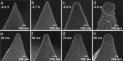
You can also read