VERIFICATION OF FIRMWARE CONTROLLED NVME HOST
←
→
Page content transcription
If your browser does not render page correctly, please read the page content below
International Research Journal of Engineering and Technology (IRJET) e-ISSN: 2395-0056
Volume: 08 Issue: 05 | May 2021 www.irjet.net p-ISSN: 2395-0072
VERIFICATION OF FIRMWARE CONTROLLED NVME HOST
Bishwapa Sanyal1, Namita Palecha2
1UG Student, Department of Electronics and Communication, RV College of Engineering, Bengaluru, India.
2Assistant Professor, Department of Electronics and Communication, RV College of Engineering, Bengaluru, India.
---------------------------------------------------------------------***---------------------------------------------------------------------
Abstract - NVMe™ (Non Volatile Memory Express®) is a library has many modifications as compared to the standard
new storage access and transport protocol for flash and next- SystemVerilog language like in packages, formation of
generation solid-state drives (SSDs) that delivers the highest sequences etc. UVM is developed based on an Accellera
throughput and fastest response times. The NVMe protocol standard and supports several company vendors like Xilinx
accesses flash storage via a PCIe bus, which is much faster Simulator(XSIM), Aldec, Mentor Graphics, Cadence, Synopsys
than hard disks and traditional flash architectures and unlike the previous methodologies. The UVM Class Library
delivers high bandwidth. Functional Verification is a task that also provides configuration database, component hierarchy,
ensures the implemented design conforms to the specification. transaction library model (TLM), etc. This enables the user
The Universal Verification Methodology (UVM) is a to virtually create any structure required for the testbench.
standardized methodology for verifying integrated circuit The main objective of the Universal Verification
designs and assembling test environments utilizing Methodology (UVM) is to improve productivity of the design
constrained random stimulus generation and functional by providing a platform that facilitates easier verification of
coverage methodologies of SystemVerilog. The primary the design components with a standardized representation
objective of this paper is to achieve a complete functional which can be used with different verification tools as
verification of the NVMe Soft host and ensuring that the required.
subsystem meets all the requirements and features as NVM Express (Non-volatile Memory Express) commonly
described in the specification document. In this paper, the known as NVMe is a logical-device interface specification
NVMe soft host implements an internal PCIe Device that is and transport protocol which can access solid-state drives
intended to be able to receive TLPs routed from other switch (SSDs) and flash devices. Hence it is used for accessing a
ports, and to generate TLPs destined for PCIe targets. computer's non-volatile storage media. The advantages of
Universal Verification Methodology (UVM) is used for NVMe are it delivers highest throughput and fastest
verification and simulations are carried out using Cadence response times. PCI Express (PCIe) bus can be used for the
NCsim tool. access of flash storage in NVMe protocol via a which helps it
to deliver a high-bandwidth and low-latency. NVMe can be
Key Words: Non-Volatile Memory Express (NVME), used for SSDs, multicore CPUs and gigabytes of memory.
Peripheral Component Interconnect Express (PCIE), NVMe is used in any fields for various applications like AI,
Functional Verification, Universal Verification big data, advanced analytics apps and ML and in real-time
Methodology (UVM), Layered Testbench Architecture. interaction platforms of e-commerce, finance, sales and
DevOps as it can complete more number of iterations in
1. INTRODUCTION lesser time. NVMe devices are generally available in the form
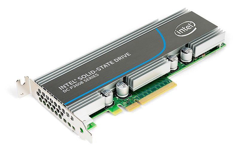
of standard-sized PCIe expansion cards which uses a U.2
Functional verification is defined as a process in which the connector and provides a four-lane PCIe interface. The Fig - 1
functional correctness of a design is determined with respect shows an Intel P3608 NVMe flash SSD, PCI-E add-in card.
to the specifications of the design. It verifies that the RTL
PCI Express (Peripheral Component Interconnect Express) is
design meets the specifications from a functional
also known as PCIe or PCI-e. It is a serial point-to-point
perspective. It assumes that the design specification is
protocol which has a very high speed capacity. It is better as
correct and cannot confirm the correctness of the design
compared to the older bus standards like AGP, PCI and PCI-X
specifications. The fundamental purpose of functional
bus and has individual serial interfaces which connects every
verification is that it ensures the implemented design
device or the endpoint to the Root complex. It has many
conforms to the specification and the failures are detected.
widespread applications like in personal computers(PC),
The identified bugs need to be corrected before the design
hard adapters of disk drives, graphics cards, Ethernet, Wi-Fi,
gets shipped to costumer.
etc. Some of the advantages of PCIe over the older standards
The UVM is an open source standardized method developed are lesser number of I/O pins, maximum bus capacity is
and maintained by Accellera which is used for the higher and scales better when connected to other bus
verification of IC designs. It is mainly used for the purpose of devices. It also has an AER mechanism for error detection
universal Verification IP interoperability. UVM is closely and an elaborate report generation. The specifications of the
related OVM from which it is mainly derived to a large extent format are made by the PCI-SIG.
which is further related to the eRM Language. The UVM class
© 2021, IRJET | Impact Factor value: 7.529 | ISO 9001:2008 Certified Journal | Page 3974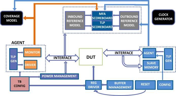
International Research Journal of Engineering and Technology (IRJET)                                    e-ISSN: 2395-0056
         Volume: 08 Issue: 05 | May 2021                www.irjet.net                                            p-ISSN: 2395-0072

                                                                        3. OVERVIEW OF PCIe

                                                                        3.1 PCIe Topology

                                                                            In PCIe, a simple tree topology is present to facilitate
                                                                        compatibility with older versions of PCI. The A simple PCIe
                                                                        topology is shown in Fig- 2. CPU is at the top of the PCIe
                                                                        topology hierarchy.
                                                                            Root complex is present at the root if the tree of the PCIe
                                                                        hierarchy is inverted. It communicates as the CPU with the
                                                                        other components of the system. It behaves as an interface
                                                                        that might be present between PCIe buses like processor
  Fig -1: Intel P3608 NVMe flash SSD, PCI-E add-in card                 interface, DRAM interface and CPU.
  (source: https://en.wikipedia.org/wiki/PCI_Express)                       Endpoints exist at the root of the branches of tree
                                                                        hierarchy. They act as the initiators and completers on the
2. LITERATURE SURVEY                                                    bus for various types of transactions. They implement only a
                                                                        single upstream port and no downstream port. Legacy PCIe
The document [1] describes the hardware independent                     Endpoint is a device that was made when the older bus like
firmware interface for managing PCI, PCI-X, and PCI                     PCI-X has to be operated on newer PCIe interface. These
Express™ systems in a host computer. The authors of [2]                 devices should have an added PCIe interface.
describe all verification features of the SystemVerilog                     Switch allows more devices to connect to attach to a
language. The advantages and disadvantages of different                 single PCIe port. They route the packets and decide the paths
language features along with descriptions of UVM features               in which the packets are directed based on the address.
are also given. The authors of [3] have developed a scheme              Bridges are used provide an interface from PCIe to other
to avoid the timing out of sync problem when PCI Bus                    older buses like PCI-X, PCI, etc.
transmits data. This has the capability to solve the problem
of high-speed data transmission between Field
Programmable Gate Array (FPGA) and PC. In [4], a few
approaches to minimize channel impedance discontinuity
and near-end/far-end crosstalk (NEXT/FEXT) are discussed.
Two channels with optimal design practices and regular
design practices are also compared and contrasted. In [5],
the verification of the PCI Express Gen5.0 transactions
between MAC and PHY layer is proposed in the work. The
RTL of PCI Express Gen5.0 is designed in SystemVerilog
language and Universal Verification Methodology (UVM) is
used for verification. Design and implementation of the
interconnection network using PCI Express is proposed in
paper [6]. The accuracy of the initial model is also verified. In                Fig -2: PCIe Topology Example (source:
paper [7], a universal verification methodology based                   https://www.mindshare.com/Books/Titles/PCI_Express_
verification environment for PCIe data link layer is built. The                              Technology_3.0)
coverage goals are achieved by enhancing the performance
                                                                        3.2 PCIe Device Layers
of verification using methods such as reusability, overriding
mechanisms. The authors of [8] have verified the
performance of SOC on a dedicated channel between                           The architecture present in PCIe is layered architecture.
peripheral component interconnect express (PCI-e) end                   The layers operate independently and hence it is easier to
point and memory. The authors of [9] have reviewed the                  adopt to newer specifications. PCIe has three main layers as
different types of bus architectures (AGP, PCI, PCI-X, PCIe).           shown in Fig- 3.
Also the description of how data transfer takes place                       Transaction layer is responsible for Transaction Layer
between the CPU to the destination in PCIe architecture is              Packet (TLP) creation on the transmit side and TLP decoding
given in this paper. Design and verification of several blocks          on the receive side. It also manages flow control and
of physical layer for PCI Express and USB is done in paper              transaction reordering.
[10].                                                                       Data Link Layer is responsible for Data Link Layer
                                                                        Packet (DLLP) creation on the transmit side and DLLP
                                                                        decoding on the receive side. It is also responsible for link
                                                                        error detection and correction. It processes the TLP received
                                                                        from transaction layer and forwards it to the physical layer
                                                                        after addition of CRC and some other bits.
© 2021, IRJET         |    Impact Factor value: 7.529               |    ISO 9001:2008 Certified Journal             |   Page 3975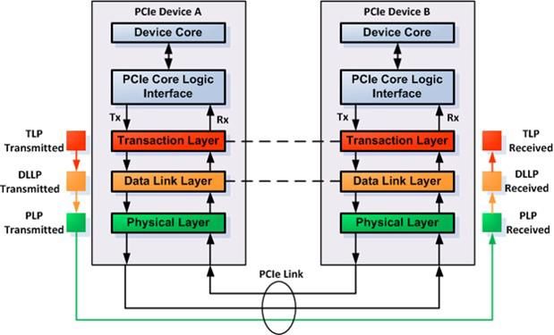
International Research Journal of Engineering and Technology (IRJET)                                   e-ISSN: 2395-0056
         Volume: 08 Issue: 05 | May 2021               www.irjet.net                                           p-ISSN: 2395-0072

                                                                             Generator, Agent, Driver, Monitor, Scoreboard,
                                                                             Checkers, etc.
                                                                        5.   After the documents are prepared, the coding for each
                                                                             of the components in both the documents are done.

          Fig -3: PCIe Device Layers (source:
https://www.mindshare.com/Books/Titles/PCI_Express_
                    Technology_3.0)
     Physical Layer processes all the different types of
packets (TLP, DLLP) transmitted to or received from the link.                     Fig -4: Basic Methodology Flowchart
It differentially clocks out the packets at the link speed and
receives it on the other side. The link initialization happens
according to the Link Training and Status State Machine                 6.  Then simulation is carried out for the environment.
(LTSSM).                                                                7.  If any new tests are found to be added, then it is added
                                                                            in the test cases document whereas if any new
                                                                            functionality is found to be added, then it is added in
3.3 PCIe Packet Types                                                       the testbench architecture document. After addition it
                                                                            has to be coded again and simulated.
     All PCIe TLPs falls in either of the two categories, posted        8. After the simulation is completed without any errors,
or non-posted TLP type. Posted TLPs may contain data                        the coverage analysis is performed.
request in the TLP but do not return any completion packet              9. While the automatic tests are executed, the code
to the requester after the transaction is complete. For Non-                coverage calculates the number of lines or branch or
posted TLPs, the requester waits for the completion TLP to                  expressions evaluated and executed. Code coverage
confirm the completion of the data or control information                   includes Line Coverage, Branch Coverage, Expression
transfer. The Memory write (MWr) and Message with and                       Coverage, Toggle Coverage and FSM Coverage.
without data (Msg/MsgD) TLPs in PCIe are posted. Other                  10. If any holes are found in the coverage model, then the
TLPs like Configuration read/write (CfgRd/CfgWr), Memory                    required test cases are added in the test cases
read (MRd) and completion TLPs are non-posted type.                         document whereas if any missing testbench support is
                                                                            found the coverage model, then the required
4. BASIC METHODOLOGY                                                        testbench is added in the testbench architecture
                                                                            document. After addition it is coded, simulated and
In order to design a complete testbench environment for                     coverage analysis is performed again.
functional verification of NVMe, the primary task is to design          11. If the coverage report is in the acceptable range, then
a flowchart for the verification methodology. The flow of                   the verification flow is terminated otherwise
verification is shown in Fig- 4. The individual steps in the                modifications are performed to bring the report to
verification flow shown in Fig- 4 are described below:                      acceptable range.
 1. The first step in the verification flow is to understand
      the specifications of Design under Test to be verified.          4.1 Testbench Architecture
 2. After understanding the specifications, the next step is
      to prepare a test case document. This test case                      The testbench architecture used for the verification of
      document should contain all the test cases possible for          NVMe soft host is shown in Fig -5 below.
      the design.                                                          For inbound path, the agent on the right side allocates
 3. Once the test case document covers more than three-                TLP space in slave memory and captures write transactions
      fourth of the functionalities, the preparation of                and stores the TLPs into respective FIFOs based on address
      testbench architecture document is started.                      ranges. For the outbound path, it writes TLPs into Slave
 4. The main components of the testbench architecture                  memory and captures read transactions to verify addresses.
      are designed. Some of the components are Transaction

© 2021, IRJET         |    Impact Factor value: 7.529              |    ISO 9001:2008 Certified Journal            |   Page 3976
International Research Journal of Engineering and Technology (IRJET)                                     e-ISSN: 2395-0056
         Volume: 08 Issue: 05 | May 2021               www.irjet.net                                            p-ISSN: 2395-0072

    The slave memory has separate space for TLP and MFA.              tool and Universal Verification Methodology (UVM) is used
MFA contains information about the TLP sent like address,             for verification.
TLP type, TLP length, etc.
    The driver on the left side will drive inbound data traffic
and outbound credit updates and the monitor captures
outbound data traffic and inbound credit updates.
    The Scoreboards are used to monitor the TLPs and
credits. The reference models are used to check the inbound
and outbound traffic.

                                                                               Fig- 7: Waveform obtained after simulation
                                                                      6. CONCLUSIONS

                                                                      The paper mainly focuses on the verification of NVME soft
                                                                      host. The primary objective of the proposed work is to
                                                                      develop a complete testbench environment for functional
                                                                      verification of the NVMe Soft host (DUT) using
                                                                      SystemVerilog and Universal Verification Methodology
                                                                      (UVM). The secondary objective is to verify that the
                                                                      subsystem meets all the requirements and features as
                                                                      mentioned in the specification document.
               Fig -5: Testbench Architecture
                                                                      The testbench is designed keeping in mind all the crucial
4.2 Test Case Coding                                                  components of a general UVM layered testbench and test
                                                                      case coding is done with the SystemVerilog and UVM. The
                                                                      simulations obtained using the Cadence NCsim reveal that
    For coding each of the test cases for verification, a
                                                                      the TLPs are successfully transmitted and received and the
standard flow is followed. The Standard UVM phases are
                                                                      functionality is successfully acheived. The states achieved by
considered while writing the flow. The general flow for
coding test cases is given below in Fig- 6.                           the LTSSM are also shown. Hence the design under test is
                                                                      successfully verified in the given work.

                                                                      REFERENCES

                                                                      [1]   PCI     Firmware         Specification     Revision    3.3,
                                                                            https://pcisig.com/specifications, 2021.
                                                                      [2]   Christian B. Spear, “SystemVerilog for Verification: A
                                                                            guide to learning the Test Bench Language Features”,
                                                                            3rd Edition, Springer Publications, 2012.
                                                                      [3]   M. Vasa, C. -L. Liao, S. Kumar, C. -H. Chen and B. Mutnury,
                                                                            "PCIe Gen-5 Design Challenges of High-Speed Servers,"
                                                                            IEEE 29th Conference on Electrical Performance of
                                                                            Electronic Packaging and Systems (EPEPS), 2020, San
              Fig- 6: Flow of test case coding                              Jose,           CA,         USA,           pp.         1-3,
                                                                            doi:10.1109/EPEPS48591.2020.9231458
5. RESULTS                                                            [4]   Y. Tao et al., "Design and implementation of high speed
                                                                            encryption and decryption system based on PCIE bus,“
The verification is done for most of the TLP types like                     IEEE 2nd International Conference on Civil Aviation
configuration read (CfgRd), memory read (MRd), memory                       Safety and Information Technology (ICCASIT), Weihai,
write (MWr), message with and without data (Msg/MsgD)                       China,          2020,       pp.         369-372,       doi:
                                                                            10.1109/ICCASIT50869.2020.9368599.
and Completion (CplD). The waveform for the simulated test
is shown below in Fig- 7. At the bottom of the waveform               [5]   G. Rohilla, D. Mathur and U. Ghanekar, "Functional
                                                                            Verification of MAC-PHY Layer of PCI Express Gen5.0
window, the edge counts for both TX packtes and RX packets
                                                                            with PIPE Interface using UVM," International
are also shown. The LTSSM states are also visible. The                      Conference for Emerging Technology (INCET), Belgaum,
transactions start only after the LTSSM is in L0 and Data Link              India,           2020,         pp.         1-5,        doi:
Layer is up. This verifies that the test is functioning as                  10.1109/INCET49848.2020.9154176.
required. The test cases are simulated using Cadence NCsim            [6]   Shim, C., Cha, Kh. & Choi, M., “Design and
                                                                            implementation of initial OpenSHMEM on PCIe NTB

© 2021, IRJET        |     Impact Factor value: 7.529             |    ISO 9001:2008 Certified Journal               |   Page 3977
International Research Journal of Engineering and Technology (IRJET)                         e-ISSN: 2395-0056
           Volume: 08 Issue: 05 | May 2021             www.irjet.net                                p-ISSN: 2395-0072

       based cloud computing”, Cluster Comput 22, Springer,
       2019, https://doi.org/10.1007/s10586-018-1707-0.
[7]    Dr. T. C. Thanuja , Akshata, “Universal verification
       methodology based verification Environment for PCIe
       data link layer” International Research Journal of
       Engineering and Technology (IRJET), Vol: 04, 2017.
[8]    S. R. Mantripragada and P. Mopuri, "Verifying
       performance of PCI express in a system for multi giga
       byte per second data transmission," International
       Conference on Communication and Electronics Systems
       (ICCES), 2017 Coimbatore, India, pp. 1-5, doi:
       10.1109/CESYS.2016.7889889.
[9]    Pamula, Vinay Kumar & Mantripragada, Sai.,
       “Implementation and verification of PCI express
       interface in a SoC”, IEICE Communications Express,
       2017, 6. 10.1587/comex.2017XBL0056.
[10]   Verma, Anuj & Dahiya, Pawan, “PCIe BUS: A State-of-the-
       Art-Review”, IOSR Journal of VLSI and Signal Processing
       (IOSR-JVSP), 2017. 7. 24-28. 10.9790/4200-
       0704012428.
[11]   Richard A Prasad, Madhusudan Kulkarni, "Design and
       verification of phy interface for PCIe GEN 3.0 and USB
       gen 3.1 using uvm methodology," International Research
       Journal of Engineering and Technology (IRJET), 2017,
       Volume: 04 Issue: 10
[12]   M. AbdElSalam, "NVMe Solid State Drive verification
       solution using HW Emulation and Virtual Device
       Technologies," 11th International Design & Test
       Symposium (IDT), Hammamet, Tunisia, 2016, pp. 47-52,
       doi: 10.1109/IDT.2016.7843013.
[13]   Y. T. Jin, S. Ahn, and S. Lee, \Performance analysis of
       nvme ssd-based all-flash array systems," in 2018 IEEE
       International Symposium on Performance Analysis of
       Systems and Software (ISPASS), 2018, pp. 12-21. doi:
       10.1109/ISPASS.2018.00010.
[14]   V. K. Pamula and S. Mantripragada, \Implementation
       and verication of pci express interface in a soc," IEICE
       Communications Express, vol. 6, Jun. 2017.
       doi:10.1587/comex.2017XBL0056.
[15]   W. Ni and J. Zhang, Research of reusability based on uvm
       verication," in 2015 IEEE 11th International Conference
       on ASIC (ASICON), 2015, pp. 1{4. doi:
       10.1109/ASICON.2015.7517189.

© 2021, IRJET          |    Impact Factor value: 7.529            |   ISO 9001:2008 Certified Journal      |   Page 3978

You can also read