7 Quantum Photonics with Thin-Film Lithium Niobate Neil Sinclair1,2 and Marko Lončar1
←
→
Page content transcription
If your browser does not render page correctly, please read the page content below
Journal of Physics: Photonics (2021) ######                                                      Roadmap

7 – Quantum Photonics with Thin-Film Lithium Niobate
Neil Sinclair1,2 and Marko Lončar1
1John
    A. Paulson School of Engineering and Applied Sciences, Harvard University,
Cambridge, Massachusetts 02138, USA
2Divisionof Physics, Mathematics and Astronomy, and Alliance for Quantum Technologies
(AQT), California Institute of Technology, Pasadena, California 91125, USA

Status

Optical photons have many attractive properties for realization of quantum technologies [1]: they
exist under ambient conditions, are generally impervious to environmental noise, and, to an extent,
can be generated, manipulated and detected easily. Since they can also travel long distances without
significant loss, individual photons are well-suited for quantum key distribution, which aims to secure
messages between distant parties using quantum uncertainty. Yet, these properties of photons also
introduce challenges to realize quantum technologies that require deterministic interactions between
individual photons, e.g. for photonic quantum information processing.

Integrated photonics will play a crucial role in realizing long- (e.g. worldwide), medium- (e.g.
metropolitan- or room-sized), and short-range (e.g. inter- or intra-chip) quantum networks. However,
the performance of a photonics platform for quantum technology applications needs to be much
better than, and in some ways different from, what is required for classical applications. For example,
a quantum photonics platform needs to: (i) be ultra-low loss in order to preserve fragile quantum
states; (ii) enable precise control of the temporal and spectral profiles of photons; (iii) allow fast and
low-loss optical switches to route quantum information; (iv) be able to operate in visible and telecom
wavelengths, where many single-photon sources and quantum memories operate, and low-loss
optical fibers exist, respectively; (v) feature strong nonlinearities for efficient frequency up- and down-
conversion, quantum transduction, and entangled photon pair generation; (vi) allow integration of
photodetectors and operating electronics. Silicon and silicon-nitride, the leading integrated photonic
platforms, do not meet these requirements due to the lack of a second-order nonlinearity, which
restricts their functionality [1]. Although this could be addressed with crystal modification or
heterogeneous integration, it remains to be seen what trade-offs, e.g. in terms of efficiency and
scalability, this would encompass.

Thin film Lithium niobate (TFLN) has emerged as a promising quantum photonic platform. LN is
transparent to optical photons (band gap of ~4 eV), possesses a strong electro-optic (EO) effect,
allowing the phase of light to be rapidly varied using microwaves, and has a high second-order optical
nonlinearity that can be engineered through ferroelectric domain modulation (i.e. periodic poling) [2].
Importantly, 4” and 6” TFLN wafers have recently become commercially available, which have
stimulated interest in this exciting material platform.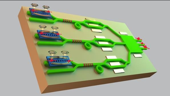
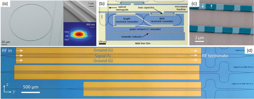
Journal of Physics: Photonics (2021) ######                                                  Roadmap

Fig 1. Integrated TFLN Photonics. (a) ultra-low loss (3 dB/m) optical waveguides and high-Q resonators
(Q ~ 10,000,000). (b) Microwave-to-optical transducer. (c) Periodically poled TFLN frequency
converter. (d) Efficient and wideband EO modulator. Reprinted with permission from [3], [9], [5], and
[4], respectively.

Current and Future Challenges

Breakthroughs in TFLN nanofabrication [3] have enabled the creation of opto-electronic components
with performance that surpasses those based on bulk LN, laying the groundwork for developing state-
of-the-art photonic quantum processors. These components (Fig. 1) range from high-bandwidth EO
modulators [4], which can enable rapid encoding of qubit states onto light or low-latency routers, to
poled waveguides and resonators that convert the wavelength of a photon [5, 6] as well as generate
non-classical states of light. These devices are particularly appealing for frequency-domain photonic
processing applications that leverage wide bandwidth of optical photons but requires high speed
modulators as well as frequency shifters/ beam splitters. The latter could be realized using an EO
photonic molecule [7, 8], formed by coupling two electrically-driven resonators

Among several challenges, one common to all on-chip photonic platforms is propagation loss. TFLN
has demonstrated ultra-low optical loss of less than 3 dB/m and on/off a chip coupling loss of 1.7 dB/
facet using TFLN waveguide tapering [10]. The insertion loss of active EO devices must be considered,
often taking into account trade-offs between efficiency and loss when designing the metal electrodes
for example.

The bandwidths of TFLN EO modulators already exceed 100 GHz and is thus sufficient for many
quantum applications. However, further reduction in drive voltages is important, especially when
considering realization of multiplexed and dynamic switch networks and gates. These must also be
interfaced with large-scale microwave circuitry for precision control and synchronization.

TFLN allows EO control of optical photons without any additional uncorrelated optical (noise) photons
being induced by the (low-energy) microwave field. However, optical frequency conversion is
accompanied by additional noise photons, e.g. due to Raman processes, which must be suppressed
for single photon-level operation. Such conversion is important for interfacing telecommunication-
wavelength photons with visible-wavelength devices, e.g. Si photodiodes and quantum memories. For
that matter, TFLN circuits which operate at wavelengths out of the infrared must be further developed
beyond that shown in proof-of-principle demonstrations. This would also benefit quantum state
Journal of Physics: Photonics (2021) ######                                                         Roadmap

generation by way of nonlinear processes such as spontaneous parametric down conversion, which
can convert a visible photon into two telecommunication wavelength photons, and squeezing.

Heterogeneous integration of devices with TFLN, an exciting prospect to realize high-bandwidth
photonic interconnects between hybrid systems, is still in its infancy. Hybrid systems include acousto-
optics, single photon detectors, or atomic interfaces on TFLN. The latter could be quantum dots,color
centers, or rare-earth ions, of which could act as single photon sources or mediate photonic gates.
Single photon detectors on TFLN must be improved beyond that shown in initial demonstrations, e.g.
with respect to efficiency (46%) and timing resolution (32 ps) [11], while also sourcing feed-forward
signals for control of later operations.

Finally, full integration of all functionalities must be realized (Fig. 2). This is especially challenging for
quantum circuits that require high-contrast interference, meaning no distinguishing information
about a photon may be introduced by the devices. Chips must be robust to environmental
disturbances, e.g. heat generated at electrodes, and operate over long periods of time in order to
allow statistically relevant measurements. The latter could be problematic due to photorefraction in
LN [2], which is a change of refractive index with high laser intensities, e.g. during optical frequency
conversion.

Advances in Science and Technology to Meet Challenges

Along with device demonstrations and improvements, photonic loss must be reduced to the levels of
the material limit, which is 0.1 dB/m for LN. This could allow optical nonlinearities at the single photon
level inside ultra-high-Q TFLN resonators. Large waveguides will help in this regard by ensuring the
optical mode does not interact with the rough sidewalls that are introduced by etching, but this will
reduce the interaction strength with LN, and hence reduce device performance. Sidewall loss can be
mitigated with further optimization at the etch step, e.g. using purer chamber gases or improved
removal of re-deposited material during dry etching. The role of surrounding materials must be
carefully examined, including absorption or surface chemistry from deposited oxides. Further,
imperfections from the TFLN production process, such as surface roughness or impurities can be
addressed by polishing and annealing. Material improvement itself must be investigated, including
stoichiometric or doped TFLN, including magnesium doping which will reduce the impact of
photorefraction. These improvements must be consistent across the wafer and be repeatable.

Other fundamentals, such as improving the electro-optic bandwidth of modulators must be
undertaken. For resonator-based modulators, this bandwidth is restricted to tens of GHz by the width
of the optical resonance and resistance-capacitance limit of the electrode. Traveling-wave modulators
allow bandwidths into the hundreds of GHz using optimized velocity and impedance matching
between microwave and light. The role of piezoelectric loss should also be accounted for. Among other
improvements, poling precision, uniformity, repeatability, and scaling must also be addressed.
Shortfalls of TFLN must be overcome with suitable heterogeneous integration, e.g. integration of
diamond color centers or by leveraging microwave-frequency quantum acoustics.
Journal of Physics: Photonics (2021) ######                                                       Roadmap

                                                        Fig. 2. Multiplexed quantum repeater node in LN
                                                        that combines diamond quantum memories with
                                                        low-loss nonlinear photonics.

Concluding Remarks

We are currently only beginning to see the potential that TFLN can provide to develop quantum
photonics. Further steps must be taken to realize advanced and fully integrated quantum
functionalities at scale. This will critically advance emerging quantum technologies, in particular
quantum networks, and will result in improvements to devices used for classical photonics and
telecommunications. Going forward, we expect light to play a significant role in quantum technology
due to its ability to carry large amounts of frequency-multiplexed qubit information in a single spatial
mode, which will allow the redundancy needed to overcome system loss and errors with a lower
scaling overhead. Thus, focus should be placed on creating and improving light-matter qubit
interfaces, a task well-suited to TFLN.

Acknowledgements
N.S. and M.L. thank Bart Machielse and Ben Pingault for manuscript comments, Boris Desiatov for the
illustration shown in Figure 2, and the rest of the Loncar group for discussions. N.S. acknowledges
support by the NSERC, INQNET research program, and by the DOE/HEP QuantISED and QCCFP
programs. M.L. acknowledges support by NSF, DARPA, ARO, AFRL, ONR, AFOSR and DOE.

References

[1] O'Brien, J., Furusawa, A. & Vuckovic, J. Photonic quantum technologies. Nature Photonics 3, 687–
695 (2009).

[2] L. Maleki and A. Matsko, Ferroelectric Crystals for Photonic Applications (Springer, 2009).

[3] M. Zhang, C. Wang, R. Cheng, A. Shams-Ansari, and M. Loncar, “Monolithic Ultrahigh-Q Lithium
Niobate Microring Resonator.” Optica, 4, 1536 (2017).
[4] Wang, C., Zhang, M., Chen, X. et al., Integrated lithium niobate electro-optic modulators operating
at CMOS-compatible voltages. Nature 562, 101–104 (2018).

[5] C. Wang, C. Langrock, A. Marandi, M. Jankowski, M. Zhang, B. Desiatov, M. M. Fejer, and M. Lončar
“Ultrahigh-efficiency wavelength conversion in nanophotonic periodically poled lithium niobate
waveguides” Optica, 5, 1438 (2018).

[6] Juanjuan Lu, Ming Li, Chang-Ling Zou, et al., Toward 1% single-photon anharmonicity with
periodically poled lithium niobate microring resonators, Optica 7, 1654-1659 (2020)
Journal of Physics: Photonics (2021) ###### Roadmap [7] Zhang, M., Wang, C., Hu, Y. et al., Electronically programmable photonic molecule. Nature Photon 13, 36–40 (2019). [8] Yaowen Hu, Mengjie Yu, Di Zhu, et al., Reconfigurable electro-optic frequency shifter. https://arxiv.org/abs/2005.09621. [9] J. Holzgrafe, N. Sinclair, D. Zhu, A. Shams-Ansari, M. Colangelo, Y. Hu, M. Zhang, K. K. Berggren, and M. Lončar. Submitted. “Cavity electro-optics in thin-film lithium niobate for efficient microwave- to-optical transduction.” Optica 7, 12, (2020). [10] He et al., Low-loss fiber-to-chip interface for lithium niobate photonic integrated circuits, Optics Letters 44, 2314 (2019). [11] Ayed Al Sayem et al., Lithium-niobate-on-insulator waveguide-integrated superconducting nanowire single-photon detectors, Applied Physics Letters 116, 15 (2020).
You can also read