Advanced Electron Microscopy of Nanophased Synthetic Polymers and Soft Complexes for Energy and Medicine Applications
←
→
Page content transcription
If your browser does not render page correctly, please read the page content below
nanomaterials

Review
Advanced Electron Microscopy of Nanophased Synthetic
Polymers and Soft Complexes for Energy and
Medicine Applications
Jihua Chen

                                          Center for Nanophase Materials Sciences, Oak Ridge National Laboratory, Oak Ridge, TN 37831, USA;
                                          chenj1@ornl.gov

                                          Abstract: After decades of developments, electron microscopy has become a powerful and irre-
                                          placeable tool in understanding the ionic, electrical, mechanical, chemical, and other functional
                                          performances of next-generation polymers and soft complexes. The recent progress in electron
                                          microscopy of nanostructured polymers and soft assemblies is important for applications in many
                                          different fields, including, but not limited to, mesoporous and nanoporous materials, absorbents,
                                          membranes, solid electrolytes, battery electrodes, ion- and electron-transporting materials, organic
                                          semiconductors, soft robotics, optoelectronic devices, biomass, soft magnetic materials, and pharma-
                                          ceutical drug design. For synthetic polymers and soft complexes, there are four main characteristics
                                          that differentiate them from their inorganic or biomacromolecular counterparts in electron microscopy
                                          studies: (1) lower contrast, (2) abundance of light elements, (3) polydispersity or nanomorphological
                                          variations, and (4) large changes induced by electron beams. Since 2011, the Center for Nanophase
                                          Materials Sciences (CNMS) at Oak Ridge National Laboratory has been working with numerous

                                   facility users on nanostructured polymer composites, block copolymers, polymer brushes, conjugated
Citation: Chen, J. Advanced Electron
                                          molecules, organic–inorganic hybrid nanomaterials, organic–inorganic interfaces, organic crystals,
Microscopy of Nanophased Synthetic        and other soft complexes. This review crystalizes some of the essential challenges, successes, failures,
Polymers and Soft Complexes for           and techniques during the process in the past ten years. It also presents some outlooks and future
Energy and Medicine Applications.         expectations on the basis of these works at the intersection of electron microscopy, soft matter, and
Nanomaterials 2021, 11, 2405. https://    artificial intelligence. Machine learning is expected to automate and facilitate image processing and
doi.org/10.3390/nano11092405              information extraction of polymer and soft hybrid nanostructures in aspects such as dose-controlled
                                          imaging and structure analysis.
Academic Editors: Nikos Boukos
and Shirley Chiang                        Keywords: nanostructures; polymers; organic crystals; electron microscopy; energy; medicine;
                                          AI (artificial intelligence)
Received: 2 July 2021
Accepted: 10 September 2021
Published: 15 September 2021

                                          1. Introduction
Publisher’s Note: MDPI stays neutral
with regard to jurisdictional claims in
                                               Electron microscopy has been of continued interest for decades, playing vital roles in
published maps and institutional affil-   revealing micro- and nanostructures as well as functionality relationships in traditional and
iations.                                  novel materials. Synthetic polymers, traditionally including four major industrial categories
                                          (adhesives, elastomers, coatings, and fibers), have intriguing structures that are often
                                          hierarchical in nature and span from the nano- to micrometer scales [1]. Synthetic polymers
                                          and their small molecule counterparts such as organic crystals and amorphous or crystalline
Copyright: © 2021 by the author.
                                          oligomers, as well as their interfaces and composite complexes with inorganic materials,
Licensee MDPI, Basel, Switzerland.
                                          now find their impacts well around us in applications such as energy storage, energy
This article is an open access article
                                          harvesting, ion and electron transport, sensors, and medicines [1–5]. Compared to inorganic
distributed under the terms and           materials, synthetic polymers and soft complexes yield poor contrast in electron microscopy
conditions of the Creative Commons        due to their intrinsically lighter elements (C, N, S, O, F, H, etc.) and severe electron beam-
Attribution (CC BY) license (https://     produced changes. In addition, it is well known that electron microscopy of synthetic
creativecommons.org/licenses/by/          polymers has very different expectations and challenges (for example, morphological
4.0/).                                    variations) than that of proteins, DNAs, and other biomacromolecules with monodispersity

Nanomaterials 2021, 11, 2405. https://doi.org/10.3390/nano11092405                                  https://www.mdpi.com/journal/nanomaterials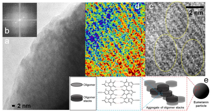
Nanomaterials 2021, 11, 2405                                                                                         2 of 25

                               and consistent 3D structures [6]. Two older [7,8] and two newer reviews [6,9] summarized
                               the progress in electron microscopy of synthetic polymers and organic materials over
                               the years.
                                    Since 2011, the Center for Nanophase Materials Sciences (CNMS) at Oak Ridge National
                               Laboratory has been working with numerous facility users on nanostructured polymer
                               composites, block copolymers, polymer brushes, conjugated molecules, organic–inorganic
                               hybrid nanomaterials, organic–inorganic interfaces, organic crystals, and other soft com-
                               plexes. This review crystalizes some of the essential challenges, successes, failures, and
                               techniques during the process in the past ten years. It also presents some outlooks and
                               future expectations on the basis of these works. Machine learning is expected to automate
                               and facilitate image processing and information extraction of polymer and soft hybrid
                               nanostructures in aspects such as dose-controlled imaging and soft structure analysis.

                               2. Comparison of Various Nanostructure Characterization Techniques
                                    The current generation of novel polymers and soft complexes often exhibits hierar-
                               chical structures that are worth exploring from the millimeter to nanometer scales, which
                               account for their cutting-edge applications in energy, medicine, and numerous other
                               fields [3,6–17]. For example, complicated structures of nanophased polymer and soft
                               complexes for biomimetics [16] and optoelectronics [17] easily span over length scales of
                               five or six orders of magnitude. This marks the importance of comprehensively under-
                               standing their structure–property relations with a host of length scales and dimensionality.
                               Figure 1 is an example of using a combination of X-ray, neutron, scanning probe, and
                               electron microscopy in studying the crystallization of a benchmark small molecule organic
                               semiconductor, 6,13-Bis(triisopropylsilylethynyl)pentacene (TIPS-PEN), in the presence
                               of a polystyrene additive with varied chain architectures (star, centipede, and linear) for
                               charge transport improvements [10]. In Figure 1A–C, cross-sectional silicon mapping
                               reveals vertical phase separation of TIPS-PEN/polystyrene composite layers on silicon
                               wafer substrates that have thermally grown SiO2 layers.

                               2.1. Probes: Tip, Electron, Ion, X-ray, and Neutron
                                    The probes that we use can play a fundamental role in the nanostructural information
                               extraction process. A previous review on nanostructures of organic solar cells elaborated
                               on the differences of various common probes in terms of their strengths and limitations [2].
                               Scanning probes are based on tip–sample interactions and rely on close physical proximity,
                               thus belonging to surface characterization techniques, which can be distinguishable from
                               the other probes that are discussed here. Electrons, ions, X-ray photons, and neutrons are
                               of variable energies and penetrating powers. Among these four penetrating probes, the
                               interaction intensities between the probe and sample generally decrease in order from ion,
                               through electron and X-ray, to neutron [2]. In other words, electron microscopy can induce
                               significant sample changes more quickly than X-ray or neutron experiments. At the same
                               time, if the beam-induced changes can be monitored and managed effectively, electron
                               microscopy may offer nanostructural information more speedily.
                                    Electron–polymer interaction is acceleration voltage-dependent [8], and the resistance
                               of polymers to electron beam-produced microstructural changes is proportional to their
                               thermal stability, which can be a function of their melting temperature, glass transition
                               temperature, or degradation temperature [7,8]. For example, synthetic polymers with π–π
                               structures are more likely to maintain their structural integrity under the same electron
                               beam exposure than those with only C–H2 backbones [7]. How to deal with the higher
                               sample–probe interaction remains the key to success in nanostructural analysis of synthetic
                               polymers and soft complexes in electron microscopy.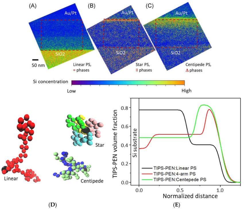
Nanomaterials 2021, 11, 2405                                                                                                   3 of 25

                               Figure 1. Cross-section EFTEM Si element mapping reveals through-thickness concentration pro-
                               files of Si-containing TIPS-PEN in blend films with various PS binders: (A) linear, (B) 4-arm star,
                               and (C) centipede. The interface of each blend film with SiO2 /Si is referred to as the bottom,
                               while the top surface (also referred to as an air interface) is coated with Au/Pt. Images (A) and
                               (C) clearly visualize vertical (=) and gradient (∆) phase segregation, respectively, while mapping of a
                               TIPS-PEN-rich domain in a lateral (II) star PS blend film (B) shows a high TIPS-PEN concentration
                               at the top. EFTEM, energy-filtered transmission electron microscopy; PS, polystyrene; TIPS-PEN,
                               6,13-bis(triisopropylsilylethynyl)-pentacene. (D) Typical bead conformations of three PSs. The central
                               beads are colored black in all three, while side chain beads are represented by different colors in
                               the star and centipede models. (E) Volume fraction profiles of TIPS-PEN in blend films, calculated
                               from neutron reflectivity. Distance from the substrate surface is normalized against film thickness.
                               TIPS-PEN, 6,13-bis(triisopropylsilylethynyl)-pentacene. Reproduced from [10] under the terms of the
                               Creative Commons CC BY license [18]. No changes have been made.

                                    The probe size generally increases in order from electron, through X-ray, to neutron [2].
                               This means the sampling area (or statistically averaged area) increases from electron,
                               through X-ray, to neutron. The highest achievable spatial resolution may not be the most
                               important factor to consider in many cases because there are many other factors that come
                               into play, such as sample preparation with proper structural preservation, the length scale
                               transition in hierarchical structures, the match of features and the sampling area, and the
                               differences between the surface and bulk morphology due to nanoconfinement effects.
                                    According to the acceleration voltage-dependent wavelength of an electron,

                                                                                    h
                                                                           λ= √                                                   (1)
                                                                                  2meV

                               (h is Plank’s constant, m is the electron mass, e is the electronic charge, and V stands for the
                               acceleration voltage of the microscope), the wavelength of electrons in electron microscopes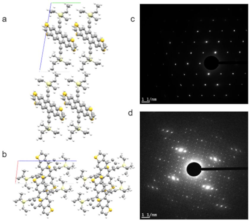
Nanomaterials 2021, 11, 2405                                                                                          4 of 25

                               is 0.017 nm for 5 kV, and 0.0027 nm for 200 kV, as compared to the infrared wavelength of
                               700–1000 nm, the visible light wavelength of 400–700 nm, the ultraviolet light wavelength
                               of 100–400 nm, and the copper K-alpha wavelength used in X-ray diffraction of 0.154 nm,
                               as well as a typical neutron wavelength in neutron scattering or diffraction experiments on
                               the order of 0.1 nm [2,7,8].

                               2.2. Connecting Real and Reciprocal Space
                                    Nanostructural characterization techniques in real space are highly complementary to
                               those in reciprocal space. There is a necessity to confirm the nanostructural information
                               extracted from one and the other.
                                    Scanning probes are intrinsically real-space techniques, although efforts are underway
                               to combine other characterization tools with them. X-ray and neutron are intrinsically
                               reciprocal space techniques but can be converted into real-space microscopy-type variations.
                               Electron microscopy covers both real and reciprocal space techniques [2,6–10,19] by itself,
                               offering a wide range of experiments at sample surfaces (scanning electron microscopy,
                               SEM, and energy-dispersive X-ray spectroscopy, EDX), or the cross-sample thickness
                               (transmission electron microscopy, TEM, and scanning transmission electron microscopy,
                               STEM). Energy loss features can be used for electron energy loss spectroscopy (EELS). With
                               pixel-by-pixel signal analysis, it is possible to use energy-filtered TEM (EFTEM) to map the
                               features of electron energy loss spectra [6,9,20]. Selected area electron diffraction (SAED)
                               and dark-field (DF) imaging may be used in parallel to achieve nanoscale characterization
                               in both reciprocal and real space, if the experiments can be performed before significant
                               structural changes happen under the electron beam.

                               2.3. Cryotome, Cryo-Holder, Cryo-Chamber, and Low Dose
                                     For electron microscopy of synthetic polymers and soft complexes, the prefix “cryo”
                               appears frequently, which requires additional attention and clarification.
                                     A cryotome is a microtome tool for samples with glass transition temperatures lower
                               than room temperature [6–9,20]. For example, elastomers, gels, rubbery materials, and
                               cells may require a cryotome to preserve their natural structures and prevent deformation
                               during the sample preparation process.
                                     A cryo-holder is useful in lowering the sample temperature during TEM experiments.
                               By a cryo-holder alone, the sample temperature during TEM experiments may not be
                               able to reach and maintain the liquid nitrogen temperature [6–9,20]. A surrounding cryo-
                               chamber inside the TEM itself is usually designed for carrying out this trick, which is a
                               requirement for cryo-plunged or fast-frozen liquid-form samples.
                                     The cryo-temperature can slightly slow down the lattice parameter expansion and
                               degradation of beam-sensitive materials under electron beams; however, it may not extend
                               the end-point dosage significantly [19]. Thus, the importance of low-dose imaging may not
                               be ignored, as it aims at acquiring the maximum amount of nanostructural information with
                               the lowest amount of electron dosage delivered to the sample area. As the magnification
                               increases, the electron dose delivered will increase by the power of two [8]. Identifying the
                               changing nanostructures under an electron beam, monitoring them closely, and damage
                               mitigation are always at the center of the challenging process of electron microscopy for
                               synthetic polymers and similar materials.

                               3. Sample Preparation Based on Contrast Mechanism
                                    The contrast mechanism in synthetic polymers and soft complexes plays a vital role
                               in planning their microscopy experiments from the very beginning. Choosing a different
                               contrast mechanism may mean a different type of TEM grid and grid coating, another
                               thought on the stain, and other changes in sample preparation.
                                    For synthetic polymeric and soft complexes, there are four main characteristics that
                               differentiate them from their inorganic or biomacromolecular counterparts [6–9]:
                               (1)   Lower contrast as compared to inorganics;
Nanomaterials 2021, 11, 2405 5 of 25
(2) Abundance of light elements as compared to inorganics;
(3) Polydispersity or nanomorphological variations as compared to proteins;
(4) Large changes induced by electron beams as compared to inorganics.
Items (2)–(4) also contribute to item (1). Item (2) renders EDX difficult for synthetic
polymers and soft complexes. Item (3) means techniques for biological cryo-TEM may not
be transferable, and sometimes even irrelevant. Item (4) causes every aspect of electron
microscopy to be much more challenging, spanning from EELS, EFTEM, SAED, and high-
resolution TEM (HRTEM).
Contrast in electron microscopy of synthetic polymers and soft complexes may be
satisfactorily generated by the following techniques, although each sample may be a
different case [6,8,11,13,14,20–24]:
a. Surface- or interface-induced contrast;
b. Intrinsic contrast from the increased density of crystalline domains;
c. Shadowing with an additional ultrathin coating or epitaxial growth;
d. Phase contrast that gives rises to lattice fringes;
e. Z contrast by a (high-angle) annular dark-field detector in STEM;
f. Inelastic electron scattering (EFTEM contrast) from low-energy plasmon regions and
core edges;
g. Diffraction contrast using an objective aperture;
h. Staining by iodine, a heavy metal, etc.
After deciding on a contrast mechanism, the next step is to generate samples of proper
thickness (50–100 nm) and optimal viewing quality without sacrificing real structures.
3.1. Focused Ion Beam (FIB) and Microtome
FIB is the sample preparation method of choice if the interface of interest is buried
underneath layers of other materials, or a cross-section view is desired along the direction
of the sample thickness (or out of plane) [6–9]. A FIB operation is often started with
deposition of the protective layer and is then followed by fast-paced milling, and gentle
final polishing to guarantee that the delicate sample nanomorphology is preserved after
ion bombardments and before a lift-off [6–9,25]. Alternatively, a tilting position may use
the substrate as the protective layer in the so-called shadow-FIB method [25]. FIB sample
preparation of polymer samples requires a much lower ion beam current as compared to
their metal or ceramic counterparts. According to the work by Kim, Liu, and Minor [25],
a microtomed polystyrene-block-polymethyl methacrylate (PS-b-PMMA) slice of 100 nm
thickness yielded no significant structural changes with a FIB ion beam current of 100 pA at
30 kV, outside the ion drilling area. However, with an ion beam current of 300 pA or higher,
significant distortion, wrinkling, and possible crosslinking can be observed in the polymer
thin film due to thermal damage [25]. Figure 2A is a cross-sectional TEM image of an
organic solar cell [21] processed by FIB. Layers 1–6 correspond to (1) indium tin oxide (ITO),
(2) a spin-coated poly(3,4-ethylenedioxythiophene) polystyrene sulfonate (PEDOT:PSS)
layer, (3) a low-bandgap polymer/PCBM composite layer, (4) a calcium layer, (5) an
aluminum electrode, and (6) a platinum protection layer for FIB sample preparation. The
black-dotted structures on layers 2 and 3 are likely caused by a polishing current that is
to be reduced during FIB sample preparation. The polishing also causes delamination
between layers 3 and 4, as well as an uneven thickness of layer 4.Nanomaterials 2021, 11, 2405 6 of 25
Figure 2. (A) A cross-sectional TEM image of an organic solar cell processed by FIB. Layers 1–6 correspond to (1) indium tin
oxide (ITO), (2) spin-coated poly(3,4-ethylenedioxythiophene) polystyrene sulfonate (PEDOT:PSS) layer, (3) low-bandgap
polymer/PCBM composite layer, (4) calcium layer, (5) aluminum electrode, and (6) platinum protection layer for FIB sample
preparation. The black-dotted structures on layers 2 and 3 are likely caused by a polishing current that is to be reduced
during FIB sample preparation. The polishing also causes delamination between layers 3 and 4, as well as an uneven
thickness of layer 4. The scale bar is 50 nm. This is an unpublished result related to a previously published work [21] (B).
Wavy microstructures of microtomed PBI films and the cutting lines that are vertical to them. A fast Fourier transformation
(FFT) of the left TEM image is presented on the right. The straight thin lines running from top left to bottom right are the
results of the non-smooth diamond knife edge, and the wavy curves vertical to them with larger spacings result from the
intrinsic mechanical instability of the film. The scale bar is 200 nm.
A microtome is a common tool for sectioning plastic samples [8,20]. A cryo-microtome
is required for materials with a glass transition temperature below room temperature.
Microtomed stubs are usually ideal surfaces for atomic force microscopy because a smooth
surface may be difficult to achieve for stand-alone soft materials. The microtomed samples
are typically floated on filtered water for lift-out with TEM grids [6–9,20]. A gold color and
continuous ribbon formation indicate that slices with a proper sample thickness are likely
achieved, although the optimal slice thickness is also dependent on the chemical nature of
the sample itself and the purpose of experiments (EFTEM, HRTEM, SAED, etc.) [6–9,20].
Low-dose HRTEM may require a thinner sample for better beam penetration, while too
thin a sample can increase the chance of instability during imaging. A too thick sample
may complicate or prevent accurate EFTEM experiments. A slightly thicker sample may
improve the intensities of the best acquirable low-dose SAED pattern.
Embedding of thin film or fiber-form samples is often necessary in order to reveal
their internal nanostructures as a function of the diagonal or vertical distance from the
outer surfaces [8,20]. A low-viscosity, high-strength, two-part epoxy formula is often
required to provide a robust matrix around the sample as well as enough adhesion at
the epoxy–sample interface. Even with the best possible epoxy embedding, some sample
films are intrinsically poor in mechanical performance at 50–100 nm thickness. Tearing,
folding, smaller sizes of sliced sections, and an increased electron beam sensitivity should
all be closely watched. These may be partly improved by providing a carbon film support
underneath the microtomed slices on TEM grids. Drying the TEM grids sideways through
a filter paper may prevent fragile slices from breaking apart.
The diamond knife edges of microtome machines require close monitoring and regular
maintenance (sharpening) [6–9,20]. Otherwise, a cracked edge on a diamond knife can
induce periodic artifacts or lines on sample slices, which should not be mistaken as the real
morphology of the sample. Figure 2B shows a microtomed slice of a polybenzimidazole
(PBI) film that is not so desirable. The straight thin lines running from top left to bottomNanomaterials 2021, 11, 2405 7 of 25
right are the results of a non-smooth diamond knife edge, and the wavy curves vertical to
them with larger spacings result from the intrinsic mechanical instability of the film.
3.2. Drop Casting, Physical Adsorption, In Situ Sample Growth, and Substrate Selection
Direct dispersion or in situ growth on ultrathin carbon or silicon substrates may
be suitable for samples in their powder or solution form [8,20]. Powder samples or
samples in non-solvents are typically dispersed at 1% by weight, while soluble sam-
ples are typically dispersed at 0.1–0.5% by weight since they tend to have better film
coverage [6–11,13,14,17,20,22]. Dispersions in non-solvents typically undergo an ultrason-
ication of a few minutes so that larger aggregations can break apart before settling onto
the TEM grid substrates. Direct physical adsorption is also possible by dipping TEM grids
with carbon films into powder-form samples. Even a very slight visual color change on the
carbon film suggests plenty of physical adsorption.
The current generation of commercially accessible TEM substrates offers significantly
more options than a decade ago. This made in situ formation of samples on TEM grids
possible, with or without in situ TEM. For example, chemically active functional end groups
of polymers, silanes, or other organic species can thus be covalently bonded to a silicon
window on TEM grids that is both electron-transparent and robust [14].
Holey carbons are great substrates on TEM grids because many parts of the sample
can be hung in vacuum for minimal background interferences, while continuous ultrathin
carbon films provide support for fragile and highly beam sensitive samples. Substrate films
with large openings are suitable for a sample that needs continuous imaging without crossing
metal grid bars but will suffer undesirable sample movements at higher magnifications.
3.3. Plunge Freezing
Samples involving liquid-form nanostructures require a fast freezing of the liquid
before undesirable solvent crystal formation [6,9,20]. The plunge freezing, cryo-transfer of
the sample onto TEM grids, and subsequent cryo-TEM experiments should be performed
under continuous protection of liquid nitrogen to ensure the whole process is maintained
at the liquid nitrogen temperature [6,9,20]. For aqueous samples, a hydrophilic treatment
on the TEM grid may be necessary to enhance sample wetting [6,9,20]. A cryo-chamber
surrounding the sample stage inside the cryo-TEM is often necessary to maintain the
sample temperature stable at the liquid nitrogen temperature, in addition to a liquid
nitrogen-protected cryo-sample holder.
3.4. To Stain or Not to Stain
As mentioned earlier, the polymer and soft complexes that are discussed here are
fundamentally distinguishable when compared to proteins and other subjects of biologic
cryo-TEM, in terms of polydispersity and morphological consistency [6,8,9,20]. The latter
relies on the staining and monodispersity of biological macromolecules to an evenly
distribute electron dose in a large number of identical crystals for enhanced contrast.
Selective staining can be useful if no other contrast mechanism is sufficient for identi-
fying the nanostructures of interest [6,8,9,20]. For example, a composite system may have
a nanostructured component with double bonds, which will promote the adsorption of
heavy ruthenium or osmium staining agents [6,8,9,20]. A crystalline domain with dense
packing can resist the staining agent more than its amorphous counterpart [6,8,9,20].
In other cases, it may not be desirable to stain the synthetic polymers and soft com-
plexes, since the staining agent can swell domains and cause chemical changes [6,8,9,20].
SAED, EDX, and EFTEM results may not be accurate or possible anymore. The staining-
induced morphology should be monitored as a function of the staining levels so that the
pristine structures can be differentiated from the stain-caused effects.Nanomaterials 2021, 11, 2405 8 of 25
3.5. Sample Drifting
Sample drifting in organic samples is a practical challenge that requires additional
attention. The causes of larger sample drifting in covalently or weakly bonded materi-
als as compared to inorganics can be multifold. These include large structural changes
during electron beam exposure, charge accumulation without dynamically compens-
able electrical conductivity, and localized sample heating coupled with poor thermal
conductivity [6–8,20]. Baking the sample with a lower current density at a low magni-
fication can help stabilize the region. A robust substrate or thin protective layer will
be beneficial too. Mitigation of sample drifting can be especially critical for ultrahigh
resolution imaging, or experiments requiring a longer data collection time such as three
window-based elemental mapping [6–9,20].
4. Electron Dose and Spatial Resolution
For synthetic polymers and soft complexes, a balance should be struck between the
target spatial resolution and the electron dose used for imaging or diffraction. It is known
that, given other conditions are constant, when the magnification increases by 10 times, the
electron dose delivered will increase by 100 times [8]. The impact of electron dose-induced
changes will be more and more severe as the magnification increases towards the limit of
spatial resolution. The magnification-dependent total dose is described as follows:
Dt = j M2 t, (2)
where j refers to the current density on the screen in the unit of pA/second, M is the
magnification of the microscope, and t is the exposure duration in the unit of second.
According to tens of data points collected in reference [8], the thermal stability of the
organic material or polymer has a logarithmic relationship with its total end-point dose or
critical dose:
Tm
LogDc = − B, (3)
A
where Tm is the melting temperature of the organic material or polymer, and A and B are
two constants. The values of constants A and B are experimentally determined to be about
150 and 5.7, respectively [8].
4.1. Bright Field and High Resolution
An increasing acceleration voltage between 5 and 400 kV will enhance the penetration
power of the electron beam, which also corresponds to a higher critical electron dose for
polymers and organic materials [8]. This also means that the electron–sample interaction
is stronger per single electron at 5 kV (as compared to 400 kV), yielding higher contrast
per electron, causing more damage, and allowing less electrons to travel across the sample
thickness. On the other hand, at higher voltages such as 400 kV, the electron–sample
interaction is weaker per single electron, yielding lower contrast and causing less damage
individually, but allowing more electrons to travel across the sample thickness. In other
words, the contrast at a lower kilovolt value is realized by a smaller amount of electrons,
where each has a larger electron–sample interaction, and the contrast at a higher kilovolt
value is driven by a larger amount of electrons, where each has a smaller electron–sample
interaction [8].
The following four steps highlight a routine procedure for low-dose high-resolution
TEM [7,8]:
A. Calibration of the survey, focus, and image mode;
B. Search for areas of interest in the survey mode (low magnification, low dose, and
low resolution);
C. Focus on a neighborhood area near the region of potential interest in the focus mode
(at a high magnification equivalent to that of the image mode);Nanomaterials 2021, 11, 2405 9 of 25
D. Go to image mode and allow the system to automatically take images using the
designed exposure time;
E. Thickness variation, sample drifting, and the misalignment between the survey,
focus, and image mode can contribute to a failed attempt. Each new sample may
require a new adjustment in imaging parameters.
4.2. Diffraction
The following steps are summarized for low-dose selected area electron diffraction [6,8,9,20]:
A. Set a proper camera length. Polymers and organic crystals typically have much
larger unit cells than those of ceramics and metals.
B. Perform calibration by acquiring a diffraction pattern at the camera length of choice
for a sputtered or commercially available gold (or aluminum) film. Align the beam
stop so that the pattern is free from the effect of the overly bright central beam.
Gold (111) rings should cover a large portion of the pattern to allow features from
polymers and organic crystals to show up in detail.
C. Angular relations between the SAED pattern and corresponding bright-field image
should be understood before acquiring SAED patterns from unknown samples.
D. Navigate sample position XY in diffraction mode after Z height adjustment and focusing.
E. Observe fading of SAED patterns under the electron beam.
F. Capture fading SAED patterns under the electron beam in the context of the electron
beam dosage or exposure.
G. Real-space imaging at the same location.
5. Chemical Mapping with Monitored Electron Damage
For EELS, signals of interest may include a low-eV plasmon region (for example, in
organic semiconductors) or core edges of C, F, S, N, O, and some other minor elements avail-
able in synthetic polymers and organic complexes. The following procedure is proposed for
minimizing electron dose damage in electron energy loss spectroscopy and energy-filtered
TEM [6,8,10,20,23]:
A. EELS spectrum calibration at 0 eV with minimal brightness and exposure time.
B. Choose either a low-eV plasmon region or core edges.
C. Acquire an elastic image for a region of interest as a baseline before EELS scans.
Monitor the changes after various EELS scans.
D. Spectroscopic measurements with beam damage monitoring.
E. Acquire another elastic image for a region of interest as a baseline before EFTEM mapping.
F. Use a minimal brightness and exposure time as a starter for EFTEM mapping. Blank
the beam, or turn down the brightness right after the mapping to prevent the sample
area from receiving an additional electron dosage.
G. Monitor the changes in elastic images.
H. Contrast improvements by gradually increasing the brightness and exposure time.
I. Continued monitoring of real-space images.
J. Estimate an optimal brightness and exposure time combination, in order to minimize
beam-induced changes and maximize EFTEM contrast.
EELS calibration is typically performed with an exposure time of milliseconds, which
may not lead to noticeable beam-induced changes. High-quality EELS scans on synthetic
polymers and organic complexes, however, can cause significant morphological changes
since a detail-oriented accumulative acquisition of the EELS spectrum may require a
large boost in the beam brightness as well as the duration of exposure times. The optimal
exposure time for EFTEM mapping on synthetic polymers and organic complexes is often in
the range of seconds. A longer exposure time in EFTEM mapping may require more sample
stability and drift correction after image acquisition, in addition to damage monitoring.Nanomaterials 2021, 11, 2405 10 of 25
6. Other Low-Dose Techniques and Temporal Resolution
In addition to the low-dose techniques that are described above, other approaches are
becoming available with automation and advanced time-resolved equipment. For example,
a high-speed camera such as K3 from Gatan can offer hundreds or even thousands of
frames per second [26]. Pulsed laser-based systems use pump-probe methods to study the
dynamics of beam-sensitive materials in TEM, offering a stunning temporal resolution of
femto- or picoseconds [27]. Their possibilities range from monitoring atomic movement
during phase transitions to studying the dynamics of biological structures in environmental
chambers. Alternatively, an electrical phase modulator can improve the temporal resolution
of a conventional TEM to the nano- to picosecond range [28].
“Aloof” or “Leapfrog” STEM or EELS can be programmed to collect data from regions
of interest on beam-sensitive samples [29–31]. A recent vibrational EELS study using
a monochromated and aberration-corrected STEM was able to differentiate site-specific
isotopic labels locally [32]. Scanning electron nanobeam diffraction [33] was used to map
the orientation and crystallinity of conjugated polymers.
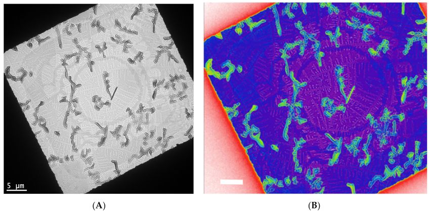
7. Morphological Variations and Hierarchical Structures
Fractal or hierarchical structures are common in synthetic polymers and soft assemblies [1–6].
In some cases, there are often more morphological variations in them than many other
categories of materials. To obtain a reliable link to their functionality, one not only needs to
understand their macroscopic structures but also microstructures, nanostructures, and the
transitions between different length scales.
In Figure 3, a controlled crystallization [17] is used to grow assemblies of function-
alized pentacene small molecules and conjugated polymers. This yields fractal crystal
domains grown at various orientations and length scales (Figure 3A). One layer consists
of crystals with lengths of 5–10 microns, while another layer consists of crystals that are
almost ten times smaller. In a color rendering based on mass thickness contrast (Figure 3B),
the group of larger crystals appears in green, while the group of small crystals is around
the purple region. Within the purple region, additional fractal-shaped, smaller crystals
are visible.
Figure 3. Bright-field TEM of a controlled crystallization of functional pentacene small molecules and conjugated polymers
yields fractal crystal domains grown at various orientations and length scales (A). One layer consists of crystals with lengths
of 5–10 microns, while another layer consists of crystals that are almost ten times smaller. In a color rendering based on
mass thickness contrast (B), the group of larger crystals is in green, while the group of small crystals is around the purple
region. These are unpublished results related to a previous published work [17].Nanomaterials 2021, 11, 2405 11 of 25
8. Case Studies
Herein, selected examples of electron microscopy work from our own lab and else-
where are grouped by the applications of synthetic polymers and soft complexes, in order
to provide glimpses of recent advances and future possibilities.
8.1. Energy Conversion and Optoelectronics
8.1.1. Polymer-Based Solar Cells
Understanding the nanomorphology is critical in order to enhance the power conver-
sion efficiency of organic solar cells [2,5]. Film floating at the water surface, FIB, and EFTEM
were used to examine the in-plane and out-of-plane nanomorphology of organic solar
cell systems with low-bandgap polymers as p-type components and fullerene derivatives
as n-type components [2,21,34–37]. The power efficiency of organic solar cells relies on
the continuous penetration of interconnected donor- and acceptor-rich domains [38–51].
Those works are complementary to and simpler than 3D tomography [52]. Many of
the low-bandgap materials contain F, N, S, O, and Si, which may be used for nanoscale
EFTEM mapping.
8.1.2. Organic Semiconductors
Conductive polymers and organic semiconductors including organic molecules with
various chemistries, sizes, and architectures (linear, block, graft, centipedes, stars, brushes,
etc.) play increasingly more important roles in sensors, photodetectors, organic light-
emitting diodes (OLEDs), and organic thin-film transistors (OTFTs) [2,5,10,34,53–72].
Many of these conjugated molecules are highly crystalline, which provides opportuni-
ties for SAED and HRTEM studies. The crystallinity, crystal orientation, and interconnec-
tion between crystalline and amorphous regions are often of keen interest for structure–
property relationships in these energy conversion or optoelectronic devices. Figure 4
presents an example of low-dose SAED patterns from a p-type solution-crystallized or-
ganic semiconductor: triethylsilyl-functionalized anthradithiophene (TES ADT). A solvent-
induced polymorphism of TES ADT is explained based on these SAED results [73].
8.1.3. Conjugated (Co)Polymers
Both synthetic and natural conjugated polymers have been of intense interest for
decades thanks to their unique optoelectronic behaviors and biofunctionality [2,5,74].
Figure 5 shows a low-dose HRTEM image of a natural conjugated polymer, melanin. A pos-
sible correlation of the high-resolution TEM results and melanin’s hierarchical structure [74]
is provided (Figure 5).
Block copolymers with a conjugated polymer component can be imaged without
staining because of the crystal packing-induced contrast [55]. For EFTEM experiments,
conjugated polymers and organic semiconductors have characteristic features at low-eV
plasmon regions (e.g., 19 eV and 30 eV for n-type and p-type materials, respectively)
that have much stronger EELS signals and may be used in combination with their core
edges [2,21,34,35].
8.2. Energy Storage
8.2.1. Meso/Nanoporous Materials and Membranes
Nanoscale interfaces are key to many transport-related phenomena [1–6]. For example,
lattice imaging was achieved by low-dose HRTEM for porous metal–organic frameworks
made from a template-free synthesis to understand their hierarchical structures and po-
tential applications [11]. Low-dose TEM was used to examine the core–shell and pore
structures of an in situ crosslinked polymer molecular sieve, as well as a mesoporous
copolymer-based sorbent [75,76]. Carbon mapping of low-dose EFTEM confirmed the
possibility of using liquid-like polymer matrices as a separation medium and a hollow
nanostructure as a transport path for a porous liquid [77].Nanomaterials 2021, 11, 2405 12 of 25
Figure 4. Bulk crystal structure of p-type small molecule organic semiconductor TES ADT: (a) viewed
down a axis, and (b) down b axis. The a, b, and c axes of the unit cell are in red, green, and blue,
respectively. This bulk crystal structure corresponds well to the [001] zone SAED patterns of TES
ADT crystalline thin films grown from THF (c). Hexane solution will induce a polymorph that is
much larger in unit cell sizes, as indicated by the [001] zone SAED patterns in (d). The simulated
views and SAED patterns shown here are unpublished results related to the work reported in [73].
Figure 5. (a) Low-dose high-resolution TEM image of a melanin sample. The largest lattices that are
visible have a spacing of 0.58 nm, which corresponds to the innermost pair of dots in the fast Fourier
transformation image. (b) A Fourier transformation of a central region in Figure 5a. (c) A zoom-in of
Figure 5a. (d) A color rendering of Figure 5c. Local crystalline packing of melanin is visible including
knitted or spiral-like structures in the highlighted circles, which correspond to the fine structures
inside the oligomer stack shown in Figure 5e. (e) The cartoon and molecular structures. Reproduced
from [74] under the terms of the Creative Commons CC BY license [18]. No changes have been made.Nanomaterials 2021, 11, 2405 13 of 25
8.2.2. Polymer Electrolyte
The current generation of solid electrolytes has intrinsic limitations at the organic–
inorganic interfaces as well as crystal grain–grain boundary interfaces [4,78,79]. A recipro-
cated cocrystallization of polyethylene oxide (PEO)/polyvinylidene difluoride (PVDF)-based
solid polymer electrolytes with an enhanced grain distribution was monitored using low-
dose SAED and low-dose EFTEM [78]. Another attempt to improve the grain–boundary
interface was to use a fullerene nanofiller [79]. Figures 6 and 7 show a series of low-dose
energy-filtered TEM images from a lithium-conducting fullerene-reinforced solid polymer
electrolyte. A 10% fullerene loading is found to enhance ion transport in a PEO/lithium bis
(trifluoromethylsulphonyl) imide (LiTFSI) system (10/1 wt.) [79]. Figure 6 shows fullerene
aggregates (white dots) with the highest contrast at an energy loss of 30 eV. Figure 7
compares the available low-dose EFTEM images of these PEO/LiTFSI composites with a
new simulation result [80] that estimates a four-state dynamical model as well as contribu-
tions from each of these four transition states to lithium ion conduction in a PEO/LiTFSI
electrolyte. Although the simulation shown in Figure 7 is on a much smaller length scale
than that in the EFTEM images, the four transition states and their larger-scale assemblies
can contribute significantly to the carbon–nitrogen or oxygen–fluoride distribution maps
in Figure 7a.
Figure 6. Low-loss EFTEM image series of a soluble fullerene/polyethylene oxide-based lithium-conducting solid electrolyte.
From left to right: 0 eV, 30 eV, and 62 eV. The images show fullerene aggregates (white dots) with the highest contrast at an
energy loss of 30 eV. These are unpublished images related to the work published in [79]. The scale bar is 10 nm.
8.2.3. Battery Interfaces
Recent lithium battery research has benefited greatly from cryogenic STEM-related
techniques. For example, the solid–liquid interphase and two types of dendrite formation
in lithium metal batteries were studied by vitrifying the liquid electrolyte for chemical
mapping [81]. The dendrites in carbonate electrolytes were found to grow along the ,
, or directions, with different nanostructures grown in different electrolytes [82].
Electrochemically deposited lithium metal was found to be amorphous with LiF in the
solid–electrolyte interface [83]. The cathode–electrolyte interface was studied with cryo-
STEM and EELS to reveal the chemical nature as well as cycling and shorting effects of
coating formation [26].
8.3. Medicine
8.3.1. Macromolecular Medicine
Synthetic polymer-based systems, such as biocompatible block copolymers, responsive
polymers, artificial vesicles, liposomes, polymer–drug conjugates, and protein–polymer
conjugates, are making extraordinary contributions to our society [3]. Exploring their
self-assembly and correlating their potential pharmaceutical performances are especially
relevant when we are counting on vaccination to fight against a global pandemic.Nanomaterials 2021, 11, 2405 14 of 25
Figure 7. (A) Elemental mapping of fullerene-modified PEO/LiTFSI (10/1 by weight) solid electrolytes by low-dose EFTEM.
The two colored images are: carbon map in red with nitrogen in green (left), and oxygen map in red with fluorine in green
(right). The two images were taken from the same region and share the same scale bar of 20 nm. These are unpublished
images related to the work published in reference [79]. (B) and (C) A four-state dynamical model learned for lithium ion
in a PEO/LiTFSI polymer electrolyte. (B) Structure of the PEO/LiTFSI polymer electrolyte. (C) Contribution from each
transition to lithium ion conduction. Each bar denotes the percentage that the transition from state i to state j contributes to
the overall lithium ion conduction. The error bars report the 95% confidence interval from four independent trajectories in
the test data. Figure 7B,C reproduced from [80], under the terms of the Creative Commons CC BY license [18]. No changes
have been made.
Bulk TEM and solution-state TEM are important tools for block copolymers, combs,
centipedes, stars, cyclics, peptides, and polypeptoids, which have many potential applica-
tions including in the medical field [22,84–93].
Low-dose EFTEM was used to resolve the structures of photo-crosslinkable poly(propylene
fumarate) (PPF)-co-polyhedral oligomeric silsesquioxane biodegradable nanocomposites
for bone repair applications [13]. Low-dose elastic images and carbon maps were able
to compare the antibody immobilization on COOH, polyethylene glycol, and a dendrimer-
functionalized silicon substrate, which contributes to a novel method for cancer detection [14].
8.3.2. Self-Assembly and Kinetics of Block or Graft Copolymers
Recently, variable-temperature liquid cell TEM was used to monitor reversible poly-
merization and polymerization-induced self-assembly (PISA) [88]. This new method
can provide many opportunities for studying kinetic solution assembly or monitoring
polymer reactions.
With the help of electron microscopy, polyacrylic acid (PAA)-b-polyisoprene (PI)- and
polyacrylic acid-b-polystyrene(PS)-based solution assemblies formed vesicle–cylinder
nanoparticles, multicomponent vesicles, and cylinder–disk particles under kineticNanomaterials 2021, 11, 2405 15 of 25
control [91]. Multicompartmental micelles of PS-b-PI-b-PAA triblock terpolymers were
formed by aqueous assembly [85]. Cryo-microtome and selective staining were used
to examine the polymer architectural effects on the phase morphology of PS-b-PI
copolymers [92]. Microphase separation was observed in comb- and centipede-type copoly-
mers of poly(n-butyl acrylate)-g-PS [22]. Solution self-assembly of triblock polymers with
fluorinated polyhedral oligomeric silsesquioxane demonstrated cylinders, nanosheets, and
patterned vesicles in sequence with increasing water content [93].
8.3.3. Self-Assembly and Kinetics of Biomacromolecules
It may not be possible to highlight all of the important progress in this category.
However, a few examples are provided here. Cryo-TEM was used to study glucose-based
coil–brush block copolymers as a function of the brush and coil length [89]. In addition, an
onion-type dendrimersome was achieved with a controlled size and number of internal
bilayers [94].
Computationally designed 29-residue peptides were found to serve as building blocks
for nanostructured lattice formation [90]. Collagen-like peptides formed nanosheets via
solution assembly [95]. Low-dose SAED was used to characterize coil-crystalline diblock
copolypeptoids [96].
8.3.4. Small Molecule Drugs
Polymorphs and crystal structures of small molecule drugs are of paramount impor-
tance to their bioavailability and pharmaceutical functions [97–100], which potentially
involve a large amount of research expense or economical loss.
For pharmaceutical crystals that are too small for X-ray studies or too difficult to use
for the growth of single crystals of large sizes, low-dose electron diffraction is favored.
For example, 3D electron diffraction and density functional theory are used to perform
structural analysis on the metastable loratadine form II [98]. Chiral isomers are associ-
ated with their bioactivities, and a dynamic refinement of low-dose electron diffraction
on micrometer crystals enabled absolute structure determination [99]. In addition, 3D
precession electron diffraction tomography was used to solve the crystal structure of two
important pharmaceutical drugs, ramelteon and tolvaptan [100]. Low-dose high-resolution
TEM was able to provide important insights on a pharmaceutical small molecule drug,
furosemide, because its defects, crystal structures, and polymorphism can play key roles in
the dissolution rate and formulation process [97].
9. AI (Artificial Intelligence) for Soft Nanostructure Analysis
Data analysis and machine learning application packages [101–105] have become
more readily available for various microscopy aspects including STEM, SEM, fluorescence
microscopy, and holography. A typical machine learning process is outlined in Figure 8,
which highlights the workflow from database formation or data collection to data cleaning,
choice of algorithms for modeling, evaluation and validation of the chosen model, and,
finally, applying the model to generate new insights [106]. Machine learning can be an
unsupervised or supervised process, based on the involvement of data labeling or human
inputs [107]. A supervised learning process is outlined in Figure 9 [107].
The nature of beam-induced sample changes in organic and polymeric materials is
rooted in the chemistry and production of these materials, which largely relies on weak forces
and covalent bonds to build up the ordered assembly and crystalline packing [7–9,19,30,108].
Due to the breakage of covalent bonds and loss of weak interactions upon overdosed
electron–sample interactions, beam-induced morphological changes can take a few dif-
ferent routes, including carbon buildup, increased crystalline defects, shrinking of crystal
dimensions, melting, crosslinking, bond breakage, mass loss, and ruptures [7–9,19,30,108].
Some of these processes can be easily mixed with the real features of the pristine sample. If
one can properly use machine learning to train a program on how to differentiate betweenNanomaterials 2021, 11, 2405 16 of 25
beam-induced effects and real features during or after experiments, the current generation
of low-dose electron microscopy techniques can be greatly improved.
Figure 8. Machine learning workflow. Reproduced from [106], under the terms of the Creative Commons CC BY license [18].
No changes have been made.
Figure 9. Supervised learning workflow. Reproduced from [107], under the terms of the Creative
Commons CC BY license [18]. No changes have been made.
In Figure 10, an example of using artificial intelligence to analyze soft matter TEM
results is shown, which involves user-defined segmentation as training sets and automated
segmentation with an algorithm of choice (such as the fast random forest model used in this
case). In another example, a convolutional neutral network algorithm, U-Net [109], was
combined with liquid-phase TEM to study the dynamics of surfactant-treated nanoparticles,
which require careful monitoring of the accumulated electron doses [110] (Figure 11).
This work showcased the possibility of using machine learning in soft matter TEM for
automated physical insight generation, which goes far beyond feature recognition and
image segmentation.Nanomaterials 2021, 11, 2405 17 of 25
Figure 10. (A) Bright-field TEM image of a polyvinylidene fluoride (PVDF)-block-polystyrene (PS)
block copolymer film showing crystalline domains in darker regions. The volume fraction of the
PVDF block is 20% in the PVDF-b-PS copolymer. (The copolymer was provided by Alex Asandei,
University of Connecticut.) (B) An attempt to classify PVDF-b-PS crystalline domains (red) and
amorphous domains (green), as well as their interfaces (purple), by using the Fiji package of Image
J and the machine learning capability of the Weka plugin. The Weka program is based on [102].
The Weka program was trained by user-predefined regions and then used a chosen algorithm to
automatically classify each pixel. For the case of PVDF-b-PS, a fast random forest method was
used to perform image segmentation, which also yields probability maps and threshold curves for
performance evaluation.
Figure 11. Statistical analysis of the diffusion, structure, and interaction landscape of gold triangular nanoprisms imaged by
liquid-phase TEM, enabled by accurate segmentation based on the trained U-Net [109] model. (a) Raw liquid-phase TEMNanomaterials 2021, 11, 2405 18 of 25
snapshot of gold triangular nanoprisms taken at a dose rate of 3.7 e– ·Å–2 ·s–1 in a SiNx liquid chamber. (b) Histogram
of the pixel intensity of the liquid-phase TEM image (a) which shows a single-peaked distribution (black line) without
a clear valley differentiating the nanoprisms and the background. Insets: Binarized images based on different signal
intensity thresholds as denoted by the arrows. (c) Binarized images of (a) different combinations of Gaussian blur and
thresholding by built-in functions in MATLAB. (d) Tracked nanoprisms (the same color denoting the same nanoprism) in
time-lapse liquid-phase TEM images based on U-Net predictions. (e) Temporal trajectories of the tracked centroid positions
of nanoprisms colored by their mean squared displacement (MSD) at a time interval of 10 s. (f) Natural logarithm of the
relative probability ln(P/P0) of displacements of the tracked nanoprisms (d) at a time interval of 0.77 s with a parabola
fitting at small displacements and a linear fitting at large displacements, where P denotes the probability of a displacement
of d, and P0 denotes the probability of d = 0. Dash lines denote the extended fitting results. (g) The 2D distribution map of
the occurrence of other nanoprisms when one nanoprism is positioned at the coordinate center. (h) The radial distribution
function and “effective” interaction landscape based on the Boltzmann inversion rule, as derived from (g). Dash lines in the
plot correspond to data from the dashed box in (g), and solid lines correspond to data from the solid box in (g). (i) The
2D histogram (right) of the relative orientations (defined by θ1 and θ2 combined, left) of two nanoprisms at a particle
center-to-center distance r < 200 nm. Scale bars: 200 nm in (a) and (e); 100 nm in (g). Reproduced from [110], under the
terms of ACS AuthorChoice License.
In addition, machine learning may be coupled with low-dose electron diffraction for
crystal symmetry determination [111], and its application in beam-sensitive materials can
have a large impact on organic crystals such as organic semiconductors, organic battery
electrodes, and pharmaceutical crystals.
10. Outlook
An additional important direction of using TEM for synthetic polymers and soft
complexes lies in tomography. A recent review paper covered this topic extensively [112].
Figure 12 is an example of using electron tomography to study the 3D porous struc-
ture of polystryrene-block-polyacrylic acid (PS-b-PAA) particles [113]. More examples
of using tomography and modeling to resolve polymer nanostructures are provided in
Figure 13 [114].
Figure 12. PS-b-PAA porous particles: (a) TEM image and (b) TEM tomography reconstruction of a 100 nm slice. Repro-
ducedfrom [113], under the terms of the Creative Commons CC BY license [18]. No changes have been made.Nanomaterials 2021, 11, 2405 19 of 25
Figure 13. 3D imaging of a PI network and SEM images of a Ni network fabricated from templating
a polylactide network. (A–C) Simulated images and (D–F) 3D reconstructions from electron tomog-
raphy of PI-b-PS-b-PLLA, PI-b-PS-b-PDLA, and PI-b-PS-b-PLA, respectively. Direct visualization
of the right-handed [112] helical locus of the PI network in (A) and (D) and the left-handed helical
locus of the PI gyroid network in (B) and (E). When an achiral PLA block is used, the structure is an
achiral diamond (F). (G–I) FESEM images of the Ni network from PI-b-PS-b-PLLA, PI-b-PS-b-PDLA,
and PI-b-PS-b-PLA, respectively, at which the Ni network takes on the handedness and volume
fraction of the particular polylactide block that is hydrolyzed. Insets show the corresponding sim-
ulated structures with dark core struts as a visual guide. Direct visualization of the Ni gyroid
network along the [111] direction demonstrates a left-handed locus in PI-b-PS-b-PLLA (G) and
right-handed helical locus in PI-b-PS-b-PDLA (H). Reproduced from [114], under the terms of the
Creative Commons CC BY license [18]. No changes have been made.
Organic small molecules and polymers form intriguing assemblies and complexes [1–5].
In an example shown in Figure 14, the addition of organic small molecules in polymers
serves the purpose of enhancing polymer characterization [115]. In another case, a ternary
soft complex facilitates the formation of promising novel nanostructures for performance
enhancement (Figure 15) [49]. In either case, low-dose TEM remains a powerful and
indispensable means to probe these soft complex structures and guide their applications in
improved materials processes.
In conclusion, electron microscopy continues to serve the goals of advancing synthetic
polymers and soft complexes by providing nanomorphological insights at interfaces and
surfaces, in bulk and in solution. These insights provide intimate connections to their
potential functionality. For synthetic polymers and soft complexes, there are four main
characteristics that differentiate them from their inorganic or biomacromolecular counter-
parts in electron microscopy studies: (1) lower contrast, (2) abundance of light elements,
(3) polydispersity or nanomorphological variations, and (4) large changes induced by elec-
tron beams. This article updates the recent progress in using soft matter TEM to advance
our understanding of synthetic polymers and soft complexes. Artificial intelligence is
expected to reinvigorate the field by bringing in improvements in soft matter TEM analysis.You can also read