ADVANCED LITHOGRAPHY TECHNICAL PROGRAM - SAN JOSE, CALIFORNIA, USA Conferences and Courses: 23-27 February 2020 Exhibition: 25-26 February 2020 - SPIE
←
→
Page content transcription
If your browser does not render page correctly, please read the page content below
ADVANCED
LITHOGRAPHY
TECHNICAL PROGRAM

SAN JOSE, CALIFORNIA, USA
Conferences and Courses:
23–27 February 2020
Exhibition:
25–26 February 2020

#SPIELitho      spie.org/al
CONNECTING MINDS.
                                                        ADVANCING LIGHT.

    ADVANCED
LITHOGRAPHY 2020
TECHNOLOGIES FOR LITHOGRAPHY R&D, DEVICES,
     TOOLS, FABRICATION, AND SERVICES

     Conferences and Courses: 23–27 February 2020
            Exhibition: 25–26 February 2020
               San Jose, California, USA

    Welcome to San Jose
                CUTTING-EDGE RESEARCH

                WORLD-CLASS SPEAKERS

               TRAINING AND EDUCATION

              FOCUSED TECHNICAL TOPICS

                        spie.org/AL

      New data laws mean you must opt in: Please sign up to receive
      email updates about this event — www.spie.org/signup
2020
                                                                                   Welcome
                                  2,100                                            For over 40 years, SPIE Advanced Lithography has played a key role in bringing together the
                                  ATTENDEES                                        micro- and nanolithography community. Lithography continues to be challenged to extend
                                                                                   into ever-shrinking generations, yet remain manufacturable and cost effective. State-of-the-art
                                                                                   processes continue with immersion lithography and multiple patterning, while EUV lithography
                                PLENARY                                            moves closer toward production readiness. At the same time, the lithography community
                                PRESENTATIONS
                                                                                   aggressively pursues alternative patterning approaches and complementary solutions. Success
                                                                                   calls for unique interdisciplinary interactions and coordinated efforts between lithographers,
                                    450                                            layout designers, materials scientists, and metrology/process control engineers to enable cost-
                                    PAPERS                                         efficient patterning solutions.
                                                                                   A full spectrum of lithography and patterning topics are encompassed by this year’s
                                    14                                             symposium across seven complementary conferences. Participants come from a broad array
                                    COURSES                                        of backgrounds to share and learn about state-of-the-art lithographic tools, resists, metrology,
                                                                                   materials, etch, design, process integration, and novel new approaches. Through provocative
                                   NETWORKING                                      panel discussions and seminars, the symposium also probes current issues being faced as
                                   EVENTS                                          we extend current methods, move toward alternative approaches, and identify new ways to
                                                                                   complement one technology with another.
                                                                                   Over the years, SPIE Advanced Lithography has provided the unique and primary forum for
                                    50
                               COMPANIES                                           meeting and interacting with a wide range of industry experts, researchers, and key players
                                                                                   working on patterning technology development. Attendance ensures that participants learn and
                                                                                   share the latest developments in areas of central importance to many vital technology fields.
                            EXHIBITION                                             All conferences are organized by current practitioners of the art—Conference Chairs, working
        Meet top suppliers showcasing the newest products,                         together with organizing committees that are experts in these fields. Numerous courses have
        innovations, and cutting-edge technologies. Discuss                        also been organized, which are taught by recognized experts from industry and academia.
                 specific requirements face-to-face.
                                                                                   Additional information is available from the many manufacturers' exhibits that allow tool
                                                                                   makers, material suppliers, and software groups to showcase new products, while interacting
                                                                                   one-on-one with participants.
                                                                                   We welcome you to San Jose for SPIE Advanced Lithography's 45th year!

SPIE is the international society for optics and photonics, an educational
not-for-profit organization founded in 1955 to advance light-based                 2020 SYMPOSIUM CHAIRS
science, engineering, and technology. The Society serves nearly 264,000
constituents from 166 countries, offering conferences and their published
proceedings, continuing education, books, journals, and the SPIE Digital                          Will Conley                                     Kafai Lai
Library in support of interdisciplinary information exchange, professional
networking, and patent precedent. SPIE provided more than $5 million in                           Cymer—An ASML                                   IBM T.J. Watson
support of education and outreach programs in 2019.                                               company (USA)                                   Research Ctr.
SPIE would like to express its deepest appreciation to the symposium
                                                                                                                                                  (USA)
chairs, conference chairs, program committees, session chairs, and
authors who have so generously given their time and advice to make this
symposium possible.
The symposium, like our other conferences and activities, would not
be possible without the dedicated contribution of our participants and
members. This program is based on commitments received up to the time
of publication and is subject to change without notice.
                                                   THIS PROGRAM IS CURRENT AS OF 10 JANUARY 2020. Find the latest on the SPIE CONFERENCE APP.                                         1
Plenary Presentations
               pages 6–7                                                      EXECUTIVE COMMITTEE
                                                                              Ofer Adan, Applied Materials (Israel)
               Don’t miss these world-class speakers discussing the           Will Conley, Cymer – An ASML company (USA)
               latest directions and most promising breakthroughs.            Nelson Felix, IBM Corp. (USA)
                                                                              Roel Gronheid, KLA-Tencor/ICOS Belgium (Belgium)
                                                                              Ryoung-Han Kim, IMEC (Belgium)
                                                                              Catherine B. Labelle, (USA)
                                                                              Kafai Lai, IBM T.J. Watson Research Ctr. (USA)
                                                                              Anna Lio, Intel Corp. (USA)
                                                                              Soichi Owa, Nikon Corp. (Japan)
                Special Events                                                Eric M. Panning, Intel Corp. (USA)

                page 8                                                        Mark C. Phillips, Intel Corp. (USA)
                                                                              John C. Robinson, KLA Corp. (USA)
                Join your peers and colleagues at these special               Martha I. Sanchez, IBM Research – Almaden (USA)
                events including the Welcome Reception, and a                 Daniel P. Sanders, IBM Research – Almaden (USA)
                Panel Discussion: EUV Lithography Perspective:                Richard Wise, Lam Research Corp. (USA)
                From the Beginning to HVM, and symposium-wide                 Chi-Min Yuan, NXP Semiconductors (USA)
                Panel Discussion.
                                                                              ADVISORY COMMITTEE
                                                                              Robert D. Allen, IBM Research - Almaden (USA)
                                                                              William H. Arnold, ASML US, Inc. (USA)
               Award Announcements                                            Timothy A. Brunner, GLOBALFOUNDRIES Inc. (USA)

               page 9                                                         Ralph R. Dammel, EMD Performance Materials Corp. (USA)
                                                                              Donis G. Flagello, Nikon Research Corp. of America (USA)

               Don't miss any of the award announcemnts and                   Harry J. Levinson, HJL Lithography (USA)
               presenations at 2020 Advanced Lithography.                     Burn Lin, National Tsing Hua Univ. (Taiwan)
                                                                              Chris A. Mack, Fractilia, LLC (USA)
                                                                              Christopher J. Progler, Photronics, Inc. (USA)
                                                                              Bruce W. Smith, Rochester Institute of Technology (USA)
                                                                              Anthony Yen, ASML US, LP (USA)

                Exhibition
                page 13
                Exhibit at SPIE Advanced Lithography. Join global
                suppliers for lithography research and development,
                devices, tools, fabrication, and services.
                                                                                                    Download the
                                                                                                    SPIE Conference App

2   SPIE ADVANCED LITHOGRAPHY 2020         ·   spie.org/al ·   #SPIELitho ·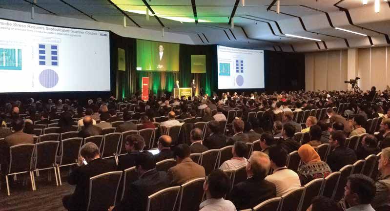
Join industry leaders to solve the latest challenges
in lithography and patterning in the semiconductor industry.
Conferences: Hear the latest advancements in optical lithography, metrology, and EUV.
Extreme Ultraviolet (EUV) Lithography XI (Felix) . . . . . . . . . . . . . . . . . . . . . . 16–45
Novel Patterning Technologies for Semiconductors, MEMS/NEMS APPLICATION TRACKS
and MOEMS 2020 (Sanchez) . . . . . . . . . . . . . . . . . . . . . . . . . . . . . . . . . . . . . . . . 16–45
Look for these icons to help
Metrology, Inspection, and Process Control for Microlithography you easily locate presentations
XXXIV (Adan) . . . . . . . . . . . . . . . . . . . . . . . . . . . . . . . . . . . . . . . . . . . . . . . . . . . . . . .16–45 you want to attend on these
hot topics. The presentations
Advances in Patterning Materials and Processes XXXVII (Gronheid) . . . . 16–34 are scheduled to prevent tim-
ing conflicts.
Optical Microlithography XXXIII (Owa) . . . . . . . . . . . . . . . . . . . . . . . . . . . . . . . 17–35
Design-Process-Technology Co-optimization for
Manufacturability XIV (Yuan) . . . . . . . . . . . . . . . . . . . . . . . . . . . . . . . . . . . . . . . . 17–45
7 CONFERENCES Stochastics Overlay Machine
Learning
Advanced Etch Technology for Nanopatterning IX (Wise) . . . . . . . . . . . . . . 17–33
Courses: Stay competitive. Optimal training for career enhancement, taught by recognized experts in industry and academia. See page 11 for schedule.
SC101 Introduction to Microlithography: Theory, Materials, SC1158 Overlay
Metrology of Image Placement (Starikov)
and Processing (Bowden, Dammel)
SC1263 Stochastic Lithography (Mack, Petersen)
SC1030 Interaction of Physical Design and Lithography Stochastics
(Yuan)
SC1264 Machine
Machine Learning for Lithography (Shiely)
SC1099 Chemistry and Lithography (Okoroanyanwu)
Learning
SC616 Practical Photoresist Processing (Dammel)
SC1100 Scatterometry in Profile, Overlay and Focus Process
Control (Cramer, Turovets) SC885 Principles and Practical Implementation of Multiple
Patterning (Dusa, Hsu)
SC111 Lithography Process Control (Levinson)
SC888 EUV Lithography (Bakshi, Ahn, Naulleau)
SC1132 Computational Basis for Advanced Lithography
Techniques (Lai) SC992 Lithography Integration for Semiconductor FEOL
& BEOL Fabrication (Lin, Zhang)
14 COURSES SC1133 Advanced concepts in Metrology Toolset Stability and
Matching (Adan)
FLOOR PLAN . . . . . . . . . . . . . . . . . . . . . . . . . . . . . . . . . . . . . 4 INDEX OF AUTHORS, CHAIRS,
AND COMMITTEE MEMBERS . . . . . . . . . . . . . . . . . . . . . . 46–59
DAILY EVENT SCHEDULE . . . . . . . . . . . . . . . . . . . . . . . . 5
GENERAL INFORMATION . . . . . . . . . . . . . . . . . . . . . . . . . . 60–62
EVENT SPONSORS . . . . . . . . . . . . . . . . . . . . . . . . . . . . . . 12
Author/Presenter Information · Policies ·
TECHNICAL CONFERENCE Food and Beverage · Onsite Services · Parking and Car Rental
SESSION SCHEDULE . . . . . . . . . . . . . . . . . . . . . . . . . 14–15
SPIE POLICIES . . . . . . . . . . . . . . . . . . . . . . . . . . . . . . . . . . . . . . . 64–65
PROCEEDINGS . . . . . . . . . . . . . . . . . . . . . . . . . . . . . . . . . . . . . . . . . 67
THIS PROGRAM IS CURRENT AS OF 10 JANUARY 2020. Find the latest on the SPIE CONFERENCE APP. 3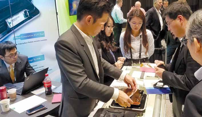
SAN JOSE CONVENTION CENTER AND MARRIOTT HOTEL
2ND LEVEL

                                                                        210D

                                              212B                      210C
    NO                                        212A
         RT
              H
                                                                        210B                      Exhibition                     Posters
                                              211B
                                              211A                      210A
                                                                                                    Hall 1                            Hall 2
                  114
                        113
                              112
                                    111

                                           Down to Rooms                  Speaker
                                              111–114                     Check-in
                   Street Level                                                                    Registration
                  Meeting Rooms                                                Food     SPIE
                                                                               Cart   Bookstore

                                                                    Think
                                                                        Tank                                                   Grand            Grand
                                          Guadalupe                                                                           Ballroom         Ballroom
                                                                                                                               220C             220B
                                                                                Salon II
                                                                     Salon I
                                                                                                                                                           Hilton Hotel
                                                  Willow
                                                  Glen III
                                                                           Marriott
                                                      Willow
                                                      Glen II                                                                            Grand
                                                        Willow
                                                                                      Salon V                                           Ballroom
                                                        Glen I
                                                                          Salon VI                                                       220A
                        Westin
                                                                                                San Jose Marriott,
                                                                                                Second Floor

                                                                                                                                                          Hyatt Place

4                                                               SPIE ADVANCED LITHOGRAPHY 2020                    ·   spie.org/al ·    #SPIELitho ·
DAILY SCHEDULE
     SUNDAY                          MONDAY                                  TUESDAY                                WEDNESDAY                             THURSDAY

Special Events
                       Welcome and Announcements;
                       Introduction of New SPIE Fellows;
                       Presentation of the Zernike Awards;
                       Presentation of the Nick Cobb Memorial
                       Scholarship, 8:00 - 8:30 AM, p. 6
                       Plenary Presentation: High performance
                       mapping for deep learning applications
                       (Rush), 8:30 - 9:10 AM, p, 6
                       Plenary Presentation: In-memory
                       computing for AI applications
                       (Eleftheriou), 8:30 AM - 9:10 AM, p. 7
                       Plenary Presentation: Process
                       technologies leading a future of
                       semiconductor memory (KIOKU)             EXHIBITION,                               EXHIBITION,
                       devices (Hashimoto), 9:50 AM - 10:30     10:00 AM - 5:00 PM                        10:00 AM - 4:00 PM
                       AM, p. 7
                                                                Women in Optics Networking Lunch,         Poster Session, 5:30 PM - 7:30 PM, p. 8
                       SPIE Fellow Member and Student           12:00 PM - 1:00 PM, p. 8
                       Luncheon, 12:30 PM - 1:30 PM, p. 8
                                                                Panel Discussion: EUV Lithography
                       Welcome and Networking Event, 6:00       Perspective: From the Beginning to
                       PM - 7:00 PM, p. 8                       HVM, 3:50 PM - 5:50 PM, p. 8
                       Intersecting the Quantum Future and      LGBTQ Lithographers Social, 5:00 PM -
                       the Semiconductor Industry (Barnes),     8:00 PM, p. 8
                       7:15 PM - 8:45 PM, p. 8
                                                                Symposium-wide Panel Discussion, 6:00
                                                                PM - 8:00 PM, p. 8

Conferences
                       Extreme Ultraviolet (EUV) Lithography XI (Felix), p. 16–45
                       Novel Patterning Technologies for Semiconductors, MEMS/NEMS and MOEMS 2020 (Sanchez), p. 16-45
                       Metrology, Inspection, and Process Control for Microlithography XXXIV (Adan), p. 16–45
                       Advances in Patterning Materials and Processes XXXVII (Gronheid), p. 16–35
                                                                 Optical Microlithography XXXIII (Owa), p. 17–35
                                                                                                         Design-Process-Technology Co-optimization for Manufacturability XIV
                                                                                                         (Yuan), p. 17–45
                                                                 Advanced Etch Technology for Nanopatterning IX (Wise), p. 17–33

    COURSES: Sunday, Monday, and Thursday
           See Course schedule page 11.
     See course descriptions and register onsite.

                           THIS PROGRAM IS CURRENT AS OF 10 JANUARY 2020. Find the latest on the SPIE CONFERENCE APP.                                                          5
WELCOME AND PLENARY PRESENTATIONS

     Distinguished
     speakers
Monday 24 February 2020 · 8:00 AM - 10:30 AM
                                                             8:30 AM - 9:10 AM                                                         9:10 AM - 9:50 AM
Location: Convention Center, Grand Ballroom 220A
                                                             High performance mapping for deep                                         In-memory computing for AI
8:00 AM - 8:30 AM                                            learning applications                                                     applications
Welcome and Announcements                                                      Allen Rush                                                               Evangelos Eleftheriou
Symposium Chairs: Will Conley, Cymer-An ASML Company (USA)                     Senior Fellow, Advanced Micro Devices, Inc.                              IBM Fellow, Cloud & Computing Infrastructure
and Kafai Lai, IBM T. J. Watson Research Ctr. (USA)                            (USA)                                                                    Zurich Research Laboratory, IBM Research -
                                                                             Deep Learning has emerged as a powerful tool                               Zürich (Switzerland)
- Introduction of New SPIE Fellows                                           for many types of applications, including detec-                            Performing computations on conventional
                                                                             tion, classification, semantic interpretation and                           von Neumann computing systems results in a
- 2020 Zernike Award Presentation to                                         many other challenging, data driven applica-                                significant amount of data being moved back
                                                                             tions. This talk addresses the challenges of the                            and forth between the physically separated
                                                             mapping of the key algorithms for deep learning onto the various          memory and processing units. This costs time and energy, and
               Winfried Kaiser,                                                                                                        constitutes an inherent performance bottleneck. It is becoming
                                                             engines and accelerators that are used in HW and SW platforms.
               Semiconductor Manufacturing Technology                                                                                  increasingly clear that for application areas such as AI (Artificial
               Business Group; Carl Zeiss SMT GmbH           Allen Rush is currently a Senior Fellow at AMD. His main respon-
                                                             sibility is chief scientist for machine learning, including strategies,   Intelligence), we need to transition to computing architectures
                                                             technology development and product planning. Previously he                in which memory and logic coexist in some form. In-memory
                                                             held a similar role for imaging and computer vision. Prior to join-       computing is a novel non-von Neumann approach where certain
- Presentation of the Nick Cobb                              ing AMD, he spent many years focusing on imaging technologies,            computational tasks are performed in the memory itself. This is
                                                             including CTO positions at several startup companies.                     enabled by the physical attributes and state dynamics of memory
  Memorial Scholarship                                                                                                                 devices, in particular resistance-based non-volatile memory
                                                                                                                                       technology. Several computational tasks such as logical opera-
                                                                                                                                       tions, arithmetic operations and even certain machine learning
                                                                                                                                       tasks can be implemented in such a computational memory
8:30 AM - 10:30 AM                                                                                                                     unit. I will present how computational memories accelerate AI
                                                                                                                                       applications and will show small- and large-scale experimental
Plenary Presentations                                                                                                                  demonstrations that perform high-level computational primitives,
                                                                                                                                       such as ultra-low-power inference engines, optimization solvers
Plenary presentations sponsored by                                                                                                     including compressed sensing and sparse coding, linear solvers
                                                                                                                                       and temporal correlation detection. Moreover, I will discuss the ef-
                                                                                                                                       ficacy of this approach to efficiently address not only inferencing
                                                                                                                                       but also training of deep neural networks. The results show that

6                                           SPIE ADVANCED LITHOGRAPHY 2020             ·   spie.org/al ·    #SPIELitho ·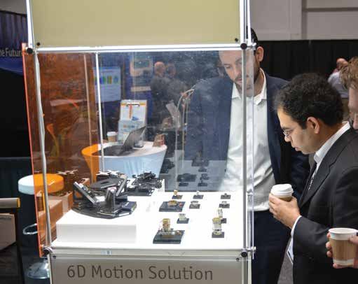
WELCOME AND PLENARY PRESENTATIONS

this co-existence of computation and storage at the nanometer          tance of non-volatile memory also continues to grow, alongside
scale could be the enabler for new, ultra-dense, low-power, and        demands for lower prices, higher performance and improved
massively parallel computing systems. Thus, by augmenting              reliability. To meet these demands, we developed revolutionary
conventional computing systems, in-memory computing could              technologies including multi-bit-per cell technology and three-
help achieve orders of magnitude improvement in performance            dimensional Flash memory technology. Recently, in addition, new
and efficiency.                                                        storage class memory (SCM) technology is being developed to
Evangelos Eleftheriou, received his Ph.D. degree in Electri-           bridge the gap between flash memory and DRAM, enabling a new
cal Engineering from Carleton University, Ottawa, Canada, in           generation of electronic devices. Manufacturing process technol-
1985. In 1986, he joined the IBM Research – Zurich laboratory          ogy must adapt quickly and efficiently to keep up with rapidly
in Rüschlikon, Switzerland, as a Research Staff Member. Since          changing design techniques. During this talk, Mr. Hashimoto will
1998, he has held various management positions and is currently        provide an overview of the key steps in the memory manufac-
responsible for the neuromorphic computing activities of IBM           turing process. In addition, Mr. Hashimoto will provide guidance
Research – Zurich. His research interests include signal process-      regarding how process and lithography engineers might approach
ing, coding, non-volatile memory technologies and emerging             the current paradigm shift in manufacturing process technology.       EQUITY
computing paradigms such as neuromorphic and in-memory                 Koji Hashimoto received an MS degree in electric engineering          Is access to
computing for AI applications. He has authored or coauthored           from Kyusyu University, Fukuoka, in 1988. After joining Toshiba       opportunities,
over 200 publications, and holds over 160 patents (granted and         ULSI Research Center, Toshiba Corporation, Kawasaki, in 1988,         fair treatment, and
pending applications). In 2002, he became a Fellow of the IEEE.        he worked on the development of megabit DRAM device tech-             advancement for all
He was co-recipient of the 2003 IEEE Communications Society            nology with Fujio Masuoka who is inventor of Flash memory.            people; it’s about
                                                                                                                                             eliminating barriers
Leonard G. Abraham Prize Paper Award. He was also co-recipient         With the first announcement of RIM type (Self aligned) Phase
                                                                                                                                             that prevent full
of the 2005 Technology Award of the Eduard Rhein Foundation.           shift mask technology in IEDM 1989, he worked on Phase shift          participation.
In 2005, he was appointed an IBM Fellow. The same year he was          mask development for sub-half micron lithography. From 1993 to
also inducted into the IBM Academy of Technology. In 2009, he          1996, he joined the quarter micron DRAM development project
was co-recipient of the IEEE CSS Control Systems Technology            with IBM and Siemens at IBM East Fishkill, NY, and worked on
Award and of the IEEE Transactions on Control Systems Technol-         lithography process development. From 1996 to 2009, he worked
ogy Outstanding Paper Award. In 2016, he received an honoris           the development of high-end lithography technology and its ap-
causa professorship from the University of Patras, Greece. In 2018,    plication to the Flash memory, DRAM, high-end CMOS, SRAM,
he was inducted into the US National Academy of Engineering            CMOS Sensors at the Process and Manufacturing Engineering
as Foreign Member.                                                     Center, Toshiba Corporation, Yokohama. From 2009 to 2013,             DIVERSITY
                                                                       for Group Manager of Advanced Lithography Process Group,              Includes all the ways in
                                                                       at the Advanced Memory Development Center, Toshiba Cor-               which people differ—
                                                                       poration, Yokkaichi, he led lithography development for 32nm          identity markers such
9:50 AM - 10:30 AM                                                     to 15nm NAND Flash memory. From 2013 to 2016, for Director            as race, ethnicity,
                                                                                                                                             gender, ability, sexual
                                                                       of Advanced Fine-patterning Development Department and
                                                                                                                                             orientation, and more.
Process technologies leading a future                                  Advanced Process Development Department, at the Advanced
of semiconductor memory (KIOKU)                                        Memory Development Center, Toshiba Corporation, Yokkaichi, he
                                                                       managed the development of lithography, dry etching and other
devices                                                                unit processes for the 3D memories. After joining to the Institute
                                                                                                                                             INCLUSION
                                                                                                                                             Goes beyond diversity:
                                                                       of Memory Technology Research and Development in 2017, for
                 Koji Hashimoto                                                                                                              it’s the act of creating
                                                                       General Manager of Process Technology Research and Develop-           an environment
                 General Manager, Process Technology Research          ment Center, Toshiba Memory Corporation, Yokkaichi, he has been       where everyone feels
                 & Development Center, KIOXIA Corp. (Japan)            top managed Research and Development of all unit processes            welcomed, respected,
                  “KIOKU” in Japanese means “memory,” but the          related to new memories. From Oct. 1th 2019, Toshiba Memory           supported, and valued.
                  word entails much more than merely recording         Corporation was changed company name to Kioxia Corporation.
                  data. KIOKU encompasses powerful, emotional          In SPIE related work, his 7 papers in SPIE Micro-lithography (1998,
                  and nostalgic memories – the type of memories        2002, 2003, 2004, 2006, 2008, 2009) and 2 papers in SPIE Asia
                  that define humanity and life. To uplift the world   (2008) were published for the first author.
with memory (KIOKU), we have developed new memory tech-
nologies to meet the demands of a rapidly changing market. As
                                                                       Break 10:30 AM to 11:00 AM
we enter the IoT era, the amount of data produced and consumed
by data centers, in industry, by surveillance, in automobiles, and
                                                                       Coffee service available until 4:00 PM                                spie.org/inclusion
so on, continues to grow. Therefore, the demand for and impor-

                                               THIS PROGRAM IS CURRENT AS OF 10 JANUARY 2020. Find the latest on the SPIE CONFERENCE APP.                               7
SPECIAL EVENTS
Technical Events                                                          Symposium-wide Panel Discussion                               Social Networking Events
Intersecting the Quantum Future                                           Tuesday 25 February 2020                                      SPIE Fellow Member and Student Luncheon
and the Semiconductor Industry                                            6:00 PM - 8:00 PM                                             Monday 24 February 2020 · 12:30 PM - 1:30 PM
                                                                          Location: Convention Center,                                  Location: Marriott, Salon V
Monday 24 February 2020 · 7:15 PM - 8:45 PM
                                                                          Grand Ballroom 220A
Location: Convention Center, Grand Ballroom 220C                                                                                        Student conference attendees and SPIE Fellow Members are invited to
                                                                          Symposium Chairs: Will Conley, Cymer–An ASML                  this engaging networking lunch. This event gives students an oppor-
Moderators: Bryan M. Barnes, NIST; Erik Hosler, PsiQuantum; R.
                                                                          company and Kafai Lai, IBM T. J. Watson Research Ctr.         tunity to network with SPIE Fellows who will share their insights into
Joseph Kline, NIST
                                                                          Moderators: Chris Mack, Fractilia, LLC and Harry J.           career paths in lithography. Lunch is complimentary. Fellow Members
Quantum computing has been a long-anticipated emerging com-                                                                             will receive a personal invitation, student seating is available on a first-
                                                                          Levinson, HJL Lithography.
putational paradigm to complement and compete with conven-                                                                              come, first-served basis.
tional CMOS technologies. The last decade has featured reports            The topic of this year’s symposium-wide panel is “A
of the initial development of using CMOS processing techniques            toast to Lithography's past: what we learned from
for qubits and the atomistic fabrication of single atom transistors.      technologies not used in HVM.” Over the years, a num-         Women in Optics Networking Lunch
Will the semiconductor industry embrace this new architype, and           ber of lithographic concepts were pursued for use in          Tuesday 25 February 2020 · 12:30 PM - 1:30 PM
if so, how? When quantum devices begin to scale as predicted,             manufacturing when optical lithography finally reached        Location: Convention Center, Room 114
will our industry be ready to integrate radically different architec-     its long-anticipated limits. While there appeared to be
tures and device structures? Are there known obstacles not yet            good reasons initially to invest substantially, in terms      Join other women in the field for informal discussions and networking
addressed that would enable the industry to more readily adopt            of people and money, in these concepts, most were not         during the scheduled lunch on Tuesday. Open to women with a paid
and benefit from today’s achievements in the laboratory? What are         ultimately adopted for use in high-volume manufactur-         registration badge. No advance registration is required. However, seat-
the emerging designs and the potential fundamental challenges             ing (HVM). In this year’s symposium-wide panel, people        ing is limited and will be granted on a first-come, first-served basis..
that are to be overcome? We have assembled a panel of experts             who were involved in developing these concepts
that will share their insights on the state-of-the-art in quantum         will share their perspectives on what lessons can be          LGBTQ+ Lithographers Social
computing as well as intellectual leaders that will share their vision    learned from their experiences.
of the eventual merger of these new technologies with our com-                                                                          Tuesday 25 February 2020 · 7:00 PM - 8:00 PM
puting capabilities today, even as lithography is approaching the                                                                       Location: Paper Plane (72 S. First Street)
near-atomic domain. Join us as we discuss the impending critical
                                                                         Poster Session
                                                                                                                                        Relax and make new friends at this informal gathering of LGBTQ+
impact of quantum computing on the semiconductor industry.               Wednesday 26 February 2020                                     lithographers and scientists! The event will be held a short walk from
                                                                         5:30 PM - 7:30 PM                                              the Convention Center at the Paper Plane cocktail bar. Allies always
Panel Discussion: EUV Lithography                                        Location: Convention Center, Hall 2                            welcome. Contact Maryann (tungmc@stanford.edu) with any questions.
Perspective: From the Beginning to HVM                                   All symposium attendees – You are invited to attend the
Tuesday 25 February 2020 · 3:50 PM - 5:50 PM                             evening Poster Session to view the high-quality posters and    Welcome and Networking Event
Location: Convention Center, Grand Ballroom 220A                         engage the authors in discussion. Enjoy light refreshments     Monday 24 February 2020 · 6:00 PM - 7:00 PM
                                                                         while networking with colleagues in your field. Authors        Location: Convention Center, Grand Ballroom Concourse
Moderatos: Nelson Felix, IBM Thomas J. Watson Research Ctr.              may set up their posters between 10:00 am and 5:00 pm
and David T. Attwood, Univ. of California, Berkeley.                     the day of their poster session. Attendees are required to     Join your colleagues at the Welcome Reception. Relax, socialize, and
SPIE will celebrate the entry of Extreme Ultraviolet Lithography         wear their conference registration badges to access the        enjoy beverages and hors-d'oeuvres on the first night of the conference.
(EUVL) into high volume manufacturing (HVM) with a special               poster session.                                                All attendees welcome.
retrospective session. Highlights will include perspectives by true      Posters that are not set up by the 5:00 pm cut-off time will   Please remember to wear your registration badge. Dress is casual.
pioneers of EUVL, the formation of early teams, the gathering of         be considered no-shows, and their manuscripts may not be
resources and organization of the industry based EUV LLC and             published. Poster authors should accompany their posters       Meet the Editor Reception
its partnering with the three national laboratory ‘Virtual National      from 5:30 to 7:30 pm to answer questions from attendees.
Laboratory’, the hand-off to SEMATECH and industry partners,             All posters and other materials must be removed no later       Wednesday 26 February 2020 · 5:30 PM - 6:30 PM
the emergence of key suppliers, and IC manufacturers’ efforts in         than 7:45 pm. Any posters or materials left behind at the      Location: Convention Center, Hall 2, (during the Poster
partnership with ASML and other suppliers.                               close of the poster session will be considered unwanted        Session)
Presenters: Hiroo Kinoshita, Bill Silfvast, Andy Hawryluk, John          and will be discarded. SPIE assumes no responsibility for      Meet Harry Levinson, Co-Editor-in-Chief of the SPIE Journal of Micro/
Carruthers, Chuck Gwyn, Peter Silverman, Rick Stulen, Don                posters left up after the end of each poster session.          Nanolithography, MEMS, and MOEMS (JM3). Please remember to wear
Sweeney, Stefan Wurm, Yan Borodovsky, Anthony Yen, Winfried                                                                             your conference registration badge to access the poster session.
Kaiser, Jos Benschop, Robert Brainard, Frank Abboud, Song-Sue            Sponsored by
Kim, and Martin van den Brink.

Sponsored by
8                                                    SPIE ADVANCED LITHOGRAPHY 2020               ·   spie.org/al ·   #SPIELitho ·
AWARD ANNOUNCEMENTS
Metrology, Inspection, Advances in Patterning Extreme Ultraviolet (EUV)
and Process Control for Materials and Processes (11326) Lithography (11323)
Microlithography (11325 ) Monday 24 February 2020 · 2:00 to 2:10 PM Thursday 27 February 2020 · 3:10 to 3:30 PM
Monday 24 February 2020 · 10:50 to 11:10 AM
Presentation of the 2020
Presentation of the 2019 Diana Presentation of the 2019 C. Grant Cymer Leadership for Best
Nyyssonen Memorial Award for Willson Award for Best Paper Student Paper Award
Best Paper in Metrology and Award Sponsored by
Award Sponsored by Presentation of the 2019
Hiroshi Ito Memorial Award for
the Best Student Paper
These Awards Sponsored by
Thursday 27 February 2020 · 9:40 to 10:00 AM
Presentation of the 2020 Karel
Urbánek Best Student Paper Award
Award Sponsored by
Presentation of the 2019 Jeffrey
Byers Memorial Best Poster Award
Award Sponsored by
TM
PLAN YOUR WEEK
GET THE FREE SPIE CONFERENCE
AND EXHIBITION APP
Find the best networking and information-gathering opportunities
with this powerful planning tool. Schedule your time in the confer-
ences…navigate the exhibition floor…make new connections.
COURTESY OF
Available for iOS and Android. Search: SPIE Conferences.
THIS PROGRAM IS CURRENT AS OF 10 JANUARY 2020. Find the latest on the SPIE CONFERENCE APP. 9Photo credit: Nguyen Khanh Hoang
Helping You
Create The Future
In 2019, SPIE provided over $5 million
in community support including
scholarships and awards, outreach
and advocacy programs, travel
grants, public policy, and educational
The International Day of Light is a global initiative highlighting to the resources.
citizens of the world the importance of light and light-based technologies We are an educational, not-for-
in their lives, for their futures, and for the development of society. profit organization that contributes
a significant percentage of revenue,
SPIE supports the International Day of Light and its annual celebration
every month, every year, without a
on 16 May. separate fundraising campaign or
administrative foundation.
SPIE IDL GRANTS
It’s what we do.
SPIE will provide seed funding up to US$3,000 to organizations
creating Day of Light activities. But we couldn’t do it without you and
the time of volunteers around the
world.
IDL RESOURCES
Inspire the next generation of
SPIE encourages communities to plan their own annual scientists and engineers by becoming
celebration on 16 May and provides various resources to help more involved with your Society’s
create an event. altruistic activities.
SPIE PHOTO CONTEST Learn more and join us.
Amateur and professional photographers alike should submit
photos demonstrating the vital role that light plays in our lives
for a chance to win US$2,500.
spie.org/get-involved
get-involved@spie.org • +1 360 676 3290
Learn more: spie.org/idl
10 SPIE ADVANCED LITHOGRAPHY 2020 · spie.org/al · #SPIELitho ·COURSES
SPIE Courses are focused, efficient training from the most
· 14 ·
experienced and accomplished minds in industry and research. SPIE
Gain knowledge from the experts and apply it directly to your daily work. COURSES
SUNDAY 23 FEBRUARY 2020 MONDAY 24 FEBRUARY 2020
SC101 Introduction to Microlithography: Theory, SC1030 Interaction of Physical Design and
Materials, and Processing (Bowden, Lithography (Yuan) 1:30 PM to 5:30 PM,
Dammel) 8:30 AM - 5:30 PM, $685 / $397 / $420 / $269 / $485
$805
SC111 Lithography Process Control (Levinson)
8:30 AM - 5:30 PM, $730 / $415 / $850 THURSDAY 27 FEBRUARY 2020
SC885 Principles and Practical Implementation SC616 Practical Photoresist Processing
of Multiple Patterning (Dusa, Hsu) 8:30 AM - (Dammel) 8:30 AM - 12:30 PM, $420 /
5:30 PM, $685 / $397 / $805 $269 / $485
SC888 EUV Lithography (Bakshi, Ahn, Naulleau)
8:30 AM - 5:30 PM, $920 / $491 / $1,040
SC992 Lithography Integration for Semiconductor
FEOL & BEOL Fabrication (Lin, Zhang) 8:30 Review course descriptions
AM - 5:30 PM, $685 / $397 / $805 onsite or online.
SC1099 Chemistry and Lithography
(Okoroanyanwu) 8:30 AM - 5:30 PM, $785 / SEE SPIE CASHIER
$437 / $905
TO REGISTER
SC1100 Scatterometry in Profile, Overlay and
Focus Process Control (Cramer,
Turovets) 1:30 PM to 5:30 PM, $420 / $269
SPIE Student Members
/ $485 receive significant
SC1132 Computational Basis for Advanced discounts on courses.
· Learn from the best. This is your opportunity for direct Lithography Techniques (Lai) 8:30 AM -
instruction from legends in the semi/litho industry, many of 12:30 PM, $420 / $269 / $485
SC1133 Advanced concepts in Metrology Toolset
whom are pioneers in their fields Stability and Matching (Adan) 1:30 PM - APPLICATION TRACKS
5:30 PM, $420 / $269 / $485 Easily find sessions on these three
· Course topics are aligned with current industry needs and trends SC1158 Metrology of Image Placement
important topics within the program. Each
conference has grouped the applicable
(Starikov) 1:30 PM to 5:30 PM, $425 / $271
presentations together and do not overlap
/ $490
· Earn CEUs for professional continuing education requirements with other conferences.
SC1263 Stochastic Lithography (Mack, Petersen)
8:30 AM - 5:30 PM, $685 / $397 / $805 • Machine Learning
spie.org/education • Stochastics
SC1264 Machine Learning for Lithography (Shiely)
Information for Course attendees: 8:30 AM - 5:30 PM, $730 / $415 / $850 • Overlay
spie.org/education/course-attendees
Prices: Members / Student Member / Non-Members
MONEY-BACK GUARANTEE CONTINUING EDUCATION UNITS
We are confident that once you experience an SPIE course for yourself you will look to us for your future SPIE is accredited by the International Association for Continuing Education and Training
education needs. However, if for any reason you are dissatisfied, we will gladly refund your money. We just (IACET) and is authorized to issue the IACET CEU.
ask that you tell us what you did not like; suggestions for improvement are always welcome.
THIS PROGRAM IS CURRENT AS OF 10 JANUARY 2020. Find the latest on the SPIE CONFERENCE APP. 11Thanks to the following sponsors for their
generous support of SPIE Advanced Lithography
TM
Promotional Partner:
Semiconductor Digest
12 SPIE ADVANCED LITHOGRAPHY 2020 · spie.org/al · #SPIELitho ·EXHIBITION
Don't miss
the Exhibition
See the industry’s most important
exhibition for lithography research
and development, devices, tools,
fabrication, and services.
TECHNOLOGIES See these companies
- Etch technology for nanoprinting Amuneal Manufacturing Corp
attocube systems Inc.
- Lithography: immersion, double patterning, Benchmark Technologies
e-beam, EUV, optical/laser, and RET C&D Semiconductor Services, Inc.
- Metrology, inspection, OPC, and process Cadence Design Systems, Inc.
control Canon U.S.A., Inc.
Carl Zeiss SMT GmbH
- Design and manufacturing software
CEROBEAR GmbH
- Materials and chemicals Cosmotec, Inc.
- Imaging equipment Coventor, Inc.
CyberOptics Corp.
- Lasers Energetiq Technology, Inc. Mentor, a Siemens Business Qoniac GmbH
- Resist materials and processing Entegris, Inc. Micro Lithography, Inc. Raith America, Inc.
Microlight SAES Group
- Nano-imprint GenISys Inc
Gudeng Precision Industrial Co., Ltd. Mitsui Chemicals America, Inc. Sage Design Automation, Inc.
- IC and chip fabrication Heidelberg Instruments Inc. Nextin Inc. SCIL Nanoimprint Solutions
- Nanoscale imaging HORIBA Instruments Inc. NTT Advanced Technology Corp. SCREEN SPE USA, LLC
ibss Group, Inc. Osiris International GmbH Seiwa Optical America Inc.
INKO Industrial Corp. Pall Corp. Semiconductor Digest
Tuesday 25 February 2020 J.A. Woollam SEQENS Shin-Etsu MicroSi, Inc.
10:00 AM - 5:00 PM JENOPTIK Light & Optics Philips Innovation Services Synopsys, Inc.
Wednesday 26 February 2020 JEOL USA Inc. PM B.V. TEL - Tokyo Electron U.S. Holdings
10:00 AM - 4:00 PM JSR Micro, Inc. POLLEN Metrology Vistec Electron Beam GmbH
Kayaku Advanced Materials, Inc. Pozzetta, Inc. XEI Scientific, Inc.
San Jose Convention Center Hall 1
Zygo Corporation
Contact SPIE Sales to Exhibit: Tel: +1 360 676 3290 · Fax: +1 360 647 1445 · SPIESales@spie.org
THIS PROGRAM IS CURRENT AS OF 10 JANUARY 2020. Find the latest on the SPIE CONFERENCE APP. 13SESSION SCHEDULE
CONFERENCE 11323 CONFERENCE 11324 CONFERENCE 11325
Extreme Ultraviolet (EUV) Novel Patterning Technologies for Metrology, Inspection, and Process
Lithography XI Semiconductors, MEMS/NEMS and Control for Microlithography XXXIV
MOEMS 2020
Monday Session 1 · Mon 11:00 AM to 12:20 PM Opening Remarks · 3:30 PM to 3:50 PM Opening Remarks and Award Announcements ·
24 February Keynote Session
Session 1 · Mon 3:50 PM to 5:10 PM
10:50 AM to 11:10 AM
Session 2 · Mon 1:20 PM to 3:20 PM Keynote Session Session 1 · Mon 11:10 AM to 12:30 PM
The Future is High NA Keynote Session
Session 3 · Mon 3:50 PM to 5:50 PM Session 2 · Mon 1:30 PM to 3:30 PM
Inorganic Resists: Joint Session with Pattern Placement and Overlay
conferences 11323 and 11326 Metrology I
Session 3 · Mon 3:50 PM to 5:30 PM
Challenges and New Methods
Tuesday Session 4 · Tue 8:00 AM to 10:00 am Session 2 · Tue 8:00 AM to 10:00 AM
25 February Stochastics: Joint Sessions with Conferences Imprint Lithography Session 4 · Tue 8:00 AM to 10:00 am
11323 and 11326 Inspection and Mass Metrology
Session 3 · Tue 10:30 AM to 12:10 PM
Session 5 · Tue 10:30 AM to 12:30 PM Scanning Probe Lithography Session 5 · Tue 10:30 AM to 12:10 PM
Stochastics of EUV Patterning High Aspect Ratio Metrology
Session 4 · Tue 1:40 PM to 3:00 PM
Session 6 · Tue 2:00 PM to 3:00 PM Nanoimprint Lithography for Semiconductors Session 6 · Tue 1:40 PM to 3:00 PM
EUV Scanner Monitoring Roughness Metrology
Session 5 · Tue 3:30 PM to 6:30 PM
EUV Poster Preview Speed Talks I · 3:00 to 3:20 PM Quantum Computing Session 7 · Tue 3:30 PM to 5:10 PM
Panel discussion · 3:50 PM to 5:50 PM New Methods: Student Session
EUV Lithography Retrospective: from the beginning
to HVM
Wednesday Session 7 · Wed 8:00 AM to 10:00 am Session 6 · Wed 8:00 AM to 10:00 AM
26 February EUV Patterning and Etch: Joint session with Multi-Beam Mask Writing Session 8 · Wed 8:00 AM to 10:00 am
conferences 11323 and 11329 Session 7 · Wed 10:30 AM to 12:10 PM 3D Profile and Shape Analysis
Session 8 · Wed 10:30 AM to 11:50 am Multi-Beam Direct Write Lithography Session 9 · Wed 10:30 AM to 12:10 PM
Progress in EUV Sources Session 8 · Wed 1:40 PM to 3:00 PM Scatterometry
Session 9 · Wed 1:20 PM to 3:40 PM 3-D Printing Session 10 · Wed 1:40 PM to 3:00 PM
Progress in EUV Masks Session 9 · Wed 3:30 PM to 5:30 PM Machine Learning
Session 10 · Wed 4:10 PM to 4:50 PM Neuromorphic Computing Session 11 · Wed 3:30 PM to 5:30 PM
EUV OPC and Modeling Pattern Placement and Overlay Metrology II
EUV Poster Preview Speed Talks II · 4:50 to 5:30 PM
Thursday Session 11 · Thu 8:00 AM to 10:20 am Session 10 · Thu 8:00 AM to 10:00 AM
27 February Atomically Precise Lithography: TopDown Session 12 · Thu 8:00 AM to 9:40 AM
EUV Resist Fundamentals
Approach Metrology for the EUV Era
Session 12 · Thu 10:50 AM to 12:30 PM
Session 11 · Thu 10:30 AM to 11:50 AM 2020 Karel Urbánek Best Student Paper Award
EUV Mask Inspection and Pellicle
Atomically Precise Lithography: BottomUp Presentation · 9:40 AM to 10:00 AM
Session 13 · Thu 1:30 PM to 3:10 PM Approach Session 13 · Thu 10:30 AM to 12:10 PM
New Concepts in EUV
Session 12 · Thu 1:40 PM to 3:20 PM Pattern Placement and Overlay Metrology III
ASML Best Student Paper Award and Closing MEMS/NEMS Session 14 · Thu 1:40 PM to 3:00 PM
Remarks · 3:10 PM to 3:30 PM
Session 13 · Thu 3:50 PM to 4:50 PM Late Breaking News
Novel Patterning and Applications
14 SPIE ADVANCED LITHOGRAPHY 2020 · spie.org/al · #SPIELitho ·SESSION SCHEDULE
CONFERENCE 11326 CONFERENCE 11327 CONFERENCE 11328 CONFERENCE 11329
Advances in Patterning Optical Microlithography Design-Process-Technology Advanced Etch Technology
Materials and Processes XXXVII XXXIII Co-optimization for for Nanopatterning IX
Manufacturability XIV
Opening Remarks and Awards
Announcements · 2:00 PM to 2:10 PM
Session 1 · Mon 2:10 PM to 3:10 PM
Keynote Session
Session 2 · Mon 3:50 PM to 5:50 PM
Inorganic Resists: Joint Session with
conferences 11323 and 11326
Session 3 · Tue 8:00 AM to 10:00 AM Session 1 · Tue 10:30 AM to 12:10 PM
Stochastics: Joint Sessions with Keynote Session and Latest Topic Session 1 · Tue 8:00 AM to 10:00 AM
Conferences 11323 and 11326 Keynote Session
Session 2 · Tue 1:40 PM to 3:20 PM
Session 4 · Tue 10:30 AM to 12:10 PM Machine Learning and Session 2 · Tue 10:30 AM to 12:10 PM
Novel Resists Computational Lithography I Materials and Etch Integration
Session 5 · Tue 1:40 PM to 3:20 PM Session 3 · Tue 3:50 PM to 5:30 PM Session 3 · Tue 1:40 PM to 3:20 PM
Fundamentals and Modeling Machine Learning and Computational Patterning and
Computational Lithography II Patterning Process Control
Session 6 · Tue 3:50 PM to 5:30 PM
Integration Session 4 · Tue 3:50 PM to 5:40 PM
Atomic Layer Etching and Novel Plasma
Techniques
Session 7 · Wed 8:10 AM to 10:00 AM Session 4 · Wed 8:00 AM to 10:00 am Session 1 · Wed 8:00 AM to 10:00 AM Session 5 · Wed 8:00 AM to 10:00 AM
Deposition-based Patterning Process Control, Resist Modeling AI and Machine Learning EUV Patterning and Etch: Joint
session with conferences 11323 and
Session 8 · Wed 10:30 AM to 12:10 PM Session 5 · Wed 10:30 AM to 12:10 PM Session 2 · Wed 10:30 AM to 12:10 PM 11329
Novel Patterning Lithography Equipment, Focus Control Advanced Designs
Session 6 · Wed 10:30 AM to 12:10 PM
Session 9 · Wed 1:40 PM to 3:00 PM Session 6 · Wed 1:40 PM to 3:00 PM Session 3 · Wed 1:40 PM to 3:10 PM Patterning Solutions for Emerging
Supplier DUV and EUV Matching Pattern Matching Applications
Session 10 · Wed 3:30 PM to 5:10 PM Session 7 · Wed 3:30 PM to Session 4 · Wed 3:40 PM to 4:40 PM Session 7 · Wed 1:40 PM to 4:00 PM
Underlayers 5:10 PM DFM by Chip Makers Advanced Patterning Integration
Overlay and CD control
Poster Preview Speed Talks · 5:10 PM to
5:30 pm
Session 5 · Thu 8:00 AM to 10:00 AM APPLICATION TRACKS
Design for Manufacturing
Easily find sessions on these three important
Session 6 · Thu 10:30 AM to 12:00 PM topics within the program. Each conference has
Device and Integration grouped the applicable presentations together
and do not overlap with other conferences.
Session 7 · Thu 1:30 PM to 3:00 PM
DPTCO from Equipment Vendors • Machine Learning
Session 8 · Thu 3:30 PM to 5:00 PM
DPTCO from EDA Vendors • Stochastics
• Overlay
THIS PROGRAM IS CURRENT AS OF 10 JANUARY 2020. Find the latest on the SPIE CONFERENCE APP. 15CONFERENCE 11323 CONFERENCE 11324 CONFERENCE 11325 CONFERENCE 11326
Monday - Thursday 24–27 February Monday - Thursday 24–27 Monday - Thursday 24–27 Monday - Wednesday 24–26
2020 • Proceedings of SPIE Vol. 11323 February 2020 • Proceedings February 2020 • Proceedings February 2020 • Proceedings
of SPIE Vol. 11324 of SPIE Vol. 11325 of SPIE Vol. 11326
Extreme Ultraviolet
Novel Patterning Metrology, Advances in
(EUV) Lithography XI
Conference Chair: Nelson M. Felix, IBM Corp.
Technologies for Inspection, and Patterning Materials
(USA)
Semiconductors, Process Control for and Processes
Conference Co-Chair: Anna Lio, Intel Corp. (USA)
Program Committee: Jos P. Benschop, ASML
MEMS/NEMS and Microlithography XXXVII
Netherlands B.V. (Netherlands); Robert L.
Brainard, SUNY CNSE/SUNYIT (USA); Martin
MOEMS 2020 XXXIV Conference Chair: Roel Gronheid, KLA-Tencor/
ICOS Belgium (Belgium)
Burkhardt, IBM Thomas J. Watson Research Conference Chair: Martha I. Sanchez, IBM Conference Chair: Ofer Adan, Applied
Ctr. (USA); Sonia Castellanos Ortega, Advanced Conference Co-Chair: Daniel P. Sanders, IBM
Research - Almaden (USA) Materials (Israel)
Research Ctr. for Nanolithography (Netherlands); Research - Almaden (USA)
Yasin Ekinci, Paul Scherrer Institut (Switzerland); Conference Co-Chair: Eric M. Panning, Intel Conference Co-Chair: John C. Robinson, KLA
Program Committee: Robert Allen, IBM
Andreas Erdmann, Fraunhofer-Institut für Corp. (USA) Corp. (USA)
Research - Almaden (USA); Gilles R. Amblard,
Integrierte Systeme und Bauelementetechnologie Program Committee: Alan D. Brodie, KLA Program Committee: John A. Allgair, BRIDG SAMSUNG Austin Semiconductor LLC (USA);
IISB (Germany); Allen H. Gabor, IBM Corp. (USA); Corp. (USA); Richard A. Farrell, Facebook Inc. (USA); Masafumi Asano, Tokyo Electron Ramakrishnan Ayothi, JSR Micro, Inc. (USA);
Emily E. Gallagher, IMEC (Belgium); Kenneth (USA); Naoya Hayashi, Dai Nippon Printing Ltd. (Japan); Benjamin D. Bunday, AMAG Ryan Callahan, FUJIFILM Electronic Materials
A. Goldberg, Lawrence Berkeley National Lab. Co., Ltd. (Japan); Daniel J. C. Herr, The Consulting, LLC (USA); Jason P. Cain, U.S.A., Inc. (USA); James F. Cameron,
(USA); Naoya Hayashi, Dai Nippon Printing Co., Univ. of North Carolina at Greensboro (USA); Advanced Micro Devices, Inc. (USA); Xiaomeng DuPont Electronics & Imaging (USA); Joy Y.
Ltd. (Japan); Eric Hendrickx, IMEC (Belgium); Tatsuhiko Higashiki, Toshiba Corp. (Japan); Chen, Taiwan Semiconductor Manufacturing Cheng, Taiwan Semiconductor Manufacturing
Soichi Inoue, Toshiba Memory Corp. (Japan); Erik R. Hosler, PsiQuantum, LLC. (USA); Co. Ltd. (Taiwan); Hugo Cramer, ASML Co. Ltd. (Taiwan); Ralph R. Dammel, EMD
Srividya Jayaram, Mentor, a Siemens Business Stephen M. Kuebler, Univ. of Central Florida Netherlands B.V. (Netherlands); Timothy Performance Materials Corp. (USA); Anuja De
(USA); Bryan S. Kasprowicz, Photronics, Inc. (USA); J. Alexander Liddle, National Institute F. Crimmins, Intel Corp. (USA); Shunsuke Silva, IBM Corp. (USA); Danilo De Simone,
(USA); Insung Kim, SAMSUNG Electronics of Standards and Technology (USA); Chi- Koshihara, Hitachi High-Technologies Corp. IMEC (Belgium); Douglas Guerrero, Brewer
Co., Ltd. (Korea, Republic of); Seong-Sue Kim, Chun Liu, IBM Corp. (USA); Hans Loeschner, (Japan); Yi-Sha Ku, Industrial Technology Science, Inc. (USA); Clifford L. Henderson,
SAMSUNG Electronics Co., Ltd. (Korea, Republic IMS Nanofabrication GmbH (Austria); John Research Institute (Taiwan); Byoung-Ho Lee, Univ. of South Florida (USA); Craig D.
of); Toshio Konishi, Toppan Printing Co., Ltd. G. Maltabes, Applied Materials GmbH & Co. SK hynix, Inc. (Korea, Republic of); Philippe Higgins, GLOBALFOUNDRIES Inc. (USA);
(Japan); Marie E. Krysak, Intel Corp. (USA); Ted KG (USA); Laurent Pain, CEA-LETI (France); Leray, IMEC (Belgium); Narender Rana, Christoph K. Hohle, Fraunhofer-Institut für
Liang, Intel Corp. (USA); Chang-Moon Lim, Ivo W. Rangelow, Technische Univ. Ilmenau Western Digital Corp. (USA); Christopher Photonische Mikrosysteme (Germany); Scott
SK Hynix, Inc. (Korea, Republic of); Luciana (Germany); Douglas J. Resnick, Canon J. Raymond, Onto Innovation Inc. (USA); W. Jessen, Texas Instruments Inc. (USA);
Meli, IBM Corp. (USA); Lawrence S. Melvin Nanotechnologies, Inc. (USA); Ricardo Ruiz, Matthew J. Sendelbach, Nova Measuring Yoshio Kawai, Shin-Etsu Chemical Co., Ltd.
III, Synopsys, Inc. (USA); Hiroaki Morimoto, Lawrence Berkeley National Lab. (USA); Instruments Inc. (USA); Richard Silver, National (Japan); Qinghuang Lin, ASML US, Inc. (USA);
Toppan Printing Co., Ltd. (Japan); Patrick P. Chandrasekhar Sarma, Intel Corp. (USA); Institute of Standards and Technology (USA); Nobuyuki N. Matsuzawa, Panasonic Corp.
Naulleau, Lawrence Berkeley National Lab. (USA); Ines A. Stolberg, Vistec Electron Beam GmbH Eric Solecky, GLOBALFOUNDRIES Inc. (USA); (Japan); Steve S. Putna, Intel Corp. (USA);
Christopher S. Ngai, Applied Materials, Inc. (Germany); Hsinyu Tsai, IBM Research - Alexander Starikov, I&I Consulting (USA); Alok Mark H. Somervell, Tokyo Electron America,
(USA); Shinji Okazaki, ALITECS Co., Ltd. (Japan); Almaden (USA); Wei Wu, The Univ. of Southern Vaid, GLOBALFOUNDRIES Inc. (USA) Inc. (USA); Jason K. Stowers, Inpria (USA);
Eric M. Panning, Intel Corp. (USA); Moshe E. California (USA) Raluca Tiron, CEA-LETI (France); Rick Uchida,
Preil, KLA Corp. (USA); Kurt G. Ronse, IMEC Tokyo Ohka Kogyo America, Inc. (USA);
(Belgium); Akiyoshi Suzuki, Gigaphoton Inc. Conference 11325 begins on page 18. Thomas I. Wallow, ASML Brion Technologies
(Japan); Anna Tchikoulaeva, Lasertec U.S.A., Inc. Conference 11324 begins on page 20.
(USA)
Zweigniederlassung Deutschland (Germany); Edita Conference Sponsor
Tejnil, Mentor Graphics Corp. (USA); Thomas I.
Conference 11326 begins on page 19.
Wallow, ASML Brion (USA); Obert R. Wood II,
GLOBALFOUNDRIES Inc. (USA)
Conference 11323 begins on page 18.
Conference Sponsor
16 SPIE ADVANCED LITHOGRAPHY 2020 · spie.org/al · #SPIELitho ·CONFERENCE 11327 CONFERENCE 11328 CONFERENCE 11329
SPEAKERS DO NOT HAVE
Tuesday - Wednesday 25–26 Wednesday - Thursday 26–27 Tuesday - Wednesday 25–26 February
THE OPTION TO USE
February 2020 • Proceedings February 2020 • Proceedings 2020 • Proceedings of SPIE Vol. 11329
THEIR OWN DEVICE
of SPIE Vol. 11327 of SPIE Vol. 11328
Advanced Etch 1. Upload in advance
Optical Design-Process- You are required to upload
Technology for your presentation file in
Microlithography Technology Co- Nanopatterning IX advance in one of two ways:
XXXIII optimization for Conference Chair: Richard S. Wise, Lam ONLINE:
Conference Chair: Soichi Owa, Nikon Corp.
(Japan)
Manufacturability Research Corp. (USA) http://spieuploads.com
(portal closes @ 5:00 PM
Conference Co-Chair: Catherine B. Labelle,
Conference Co-Chair: Mark C. Phillips, Intel XIV Intel Corp. (USA)
PST, 21 February 2020)
Corp. (USA) Program Committee: Efrain Altamirano- ONSITE AT SPEAKER
Conference Chair: Chi-Min Yuan, NXP
Program Committee: Jack Chen, Semiconductors (USA) Sánchez, IMEC (Belgium); John Arnold, IBM CHECK-IN: using your
NanoPatterning Technology Co Ltd. (Taiwan); Thomas J. Watson Research Ctr. (USA); Keun USB device, upload at
Conference Co-Chair: Ryoung-Han Kim, IMEC Hee Bai, SAMSUNG Electronics Co., Ltd.
Will Conley, Cymer, An ASML company
(Belgium)
least 2 hours before
(USA); Carlos Fonseca, Tokyo Electron (Korea, Republic of); Julie Bannister, Tokyo session or the day
America, Inc. (USA); Bernd Geh, Carl Zeiss Program Committee: Robert Aitken, ARM Electron America, Inc. (USA); Maxime Darnon, before if presenting in
SMT GmbH (USA); Yuri Granik, Mentor Inc. (USA); Jason P. Cain, Advanced Micro LN2 CNRS (Canada); Sebastian U. Engelmann,
IBM Thomas J. Watson Research Ctr. (USA);
first morning session
Graphics Corp. (USA); Harsha Grunes, Intel Devices, Inc. (USA); Luigi Capodieci, Motivo,
Corp. (USA); Toshiyuki Hisamura, Xilinx, Inc. (USA); Lifu Chang, HiSilicon Technologies Eric A. Hudson, Lam Research Corp. (USA);
Inc. (USA); Stephen D. Hsu, ASML San Co., Ltd. (USA); Neal V. Lafferty, Mentor, Kaushik A. Kumar, Tokyo Electron Ltd. (Japan); 2. Preview your
Jose (USA); Young Seog Kang, SAMSUNG a Siemens Business (USA); Ya-Chieh Lai, Qinghuang Lin, IBM Thomas J. Watson
Research Ctr. (USA); Ru-Gun Liu, Taiwan
presentation onsite
Electronics Co., Ltd. (Korea, Republic of); Cadence Design Systems, Inc. (USA); Lars W.
Sachiko Kobayashi, Toshiba Corp. (Japan); Liebmann, TEL Technology Ctr., America, LLC Semiconductor Manufacturing Co. Ltd. (Taiwan); All presenters are strongly
Jongwook Kye, SAMSUNG Electronics Co., (USA); Ru-Gun Liu, Taiwan Semiconductor Nihar Mohanty, Oculus VR, LLC (USA); Jake encouraged to visit Speaker
Ltd. (Korea, Republic of); Kafai Lai, IBM Manufacturing Co. Ltd. (Taiwan); Kevin Lucas, O’Gorman, Hitachi High Technologies America, Check-In at least 2 hours
Corp. (USA); Ken-Ichiro Mori, Canon Inc. Synopsys, Inc. (USA); Andrew R. Neureuther, Inc. (USA); Erwine Pargon, CNRS/LTM (France);
prior to their presentation to
(Japan); John S. Petersen, IMEC (USA); Univ. of California, Berkeley (USA); Shigeki Nicolas Posseme, CEA-LETI (France); Ricardo
Ruiz, Lawrence Berkeley National Lab. (USA); preview their files through the
Daniel Sarlette, Infineon Technologies Nojima, KIOXIA Corp. (Japan); David Z. Pan,
Dresden (Germany); Kunal N. Taravade, The Univ. of Texas at Austin (USA); Chul- Yuyang Sun, Mentor Graphics Corp. (USA); Ying SPIE presentation system.
Synopsys, Inc. (USA); Edita Tejnil, Mentor Hong Park, SAMSUNG Electronics Co., Ltd. Zhang, NAURA (USA); Anthony Yen, ASML US,
Graphics Corp. (USA); Geert Vandenberghe, (Korea, Republic of); Piyush Pathak, Cadence LP (USA)
IMEC (Belgium); Reinhard Voelkel, SUSS Design Systems, Inc. (USA); Michael L. Rieger,
MicroOptics SA (Switzerland); Uwe D. Zeitner, Consultant (USA); Vivek K. Singh, Intel Corp.
SPIE will record the audio
Conference 11329 begins on page 21.
Fraunhofer-Institut für Angewandte Optik und (USA); Lynn T. Wang, GLOBALFOUNDRIES plus screen content of all
Feinmechanik (Germany) Inc. (USA) presentations. Recordings
will be published on the SPIE
Conference 11327 begins on page 23. Conference 11328 begins on page 29. Digital Library with author
permission only.
Conference Sponsor
THIS PROGRAM IS CURRENT AS OF 10 JANUARY 2020. Find the latest on the SPIE CONFERENCE APP. 17Monday 24 February
CONFERENCE 11325
CONFERENCE 11323 Metrology, Inspection,
Extreme Ultraviolet (EUV) and Process Control for
Lithography XI Microlithography XXXIV
PLENARY SESSION · ROOM: CONVENTION CENTER, GRAND BALLROOM 220A · 8:00 AM TO 10:00 AM
8:00 AM to 8:30 AM · Welcome and Announcements 8:30 AM: 9:50 AM:
Symposium Chairs: Will Conley, Cymer, An ASML Company
High performance mapping for deep Process technologies
(USA), and Kafai Lai, IBM T. J. Watson Research Ctr. (USA) learning applications leading a future of
Allen Rush, Advanced Micro Devices, Inc. (USA) semiconductor memory
· Introduction of New SPIE Fellows (KIOKU) devices
· Presentation of the Zernike Award Koji Hashimoto, kioxia Corporation
(Japan)
· Presentation of the Nick Cobb Memorial Scholarship 9:10 AM:
In-memory computing for AI applications
Evangelos Eleftheriou, IBM Research - Zürich (Switzerland)
Plenary presentations sponsored by
Coffee Break · Mon 10:30 AM to 11:00 AM
SESSION 1 LOCATION: CONVENTION CENTER,
LOCATION: CONVENTION CENTER, GRAND BALLROOM 220B, 10:50 AM TO 11:10 AM
GRAND BALLROOM 220A Opening Remarks and Award
MON 11:00 AM TO 12:20 PM
Announcements
Keynote Session Session Chairs: Ofer Adan, Applied Materials Israel, Ltd. (Israel);
Session Chairs: Nelson M. Felix, IBM Thomas John C. Robinson, KLA Corp. (USA)
J. Watson Research Ctr. (USA); Anna Lio, Intel Presentation of the 2019 Diana Nyyssonen Best Paper
Corp. (USA) Award in Metrology
11:00 am: Next generation patterning using Award Sponsored by
EUV lithography (Keynote Presentation), Sam
Sivakumar, Intel Corp. (USA). . . . . . . . . . [11323-1]
11:40 am: Pushing EUV patterning to the atomic
scale (Keynote Presentation), Patrick P. Naulleau,
The Ctr. for X-Ray Optics (USA). . . . . . . [11323-2] SESSION 1 APPLICATION TRACKS
Lunch Break . . . . . . . . . Mon 12:20 pm to 1:20 pm LOCATION: CONVENTION CENTER, GRAND BALLROOM Easily find sessions on these three
220B , MON 11:10 AM TO 12:30 PM important topics within the program.
Keynote Session Each conference has grouped the
Session Chairs: Ofer Adan, Applied Materials Israel, Ltd. applicable presentations together
(Israel); John C. Robinson, KLA Corp. (USA) Overlay and do not overlap with other
11:10 am: Metrology for advanced transistor and memristor devices
conferences.
and materials (Keynote Presentation), Alain C. Diebold, Nathaniel C.
Cady, SUNY Polytechnic Institute (USA). . . . . . . . . . . . . . . . . . . . [11325-1] • Machine Learning
11:50 am: Metrology requirements driven by memory scaling (Keynote
Presentation), Cornel Bozdog, Micron Technology, Inc. (USA). [11325-100]
• Stochastics
Lunch Break . . . . . . . . . . . . . . . . . . . . . . . . . . . . Mon 12:30 pm to 1:30 pm
• Overlay
18 SPIE ADVANCED LITHOGRAPHY 2020 · spie.org/al · #SPIELitho ·Monday 24 February
CONFERENCE 11325 CONFERENCE 11326
CONFERENCE 11323 Metrology, Inspection, Advances in Patterning
Extreme Ultraviolet (EUV) and Process Control for Materials and Processes
Lithography XI Microlithography XXXIV XXXVII
SESSION 2 SESSION 2 LOCATION: CONVENTION CENTER, GRAND
LOCATION: CONVENTION CENTER, BALLROOM 220C , 2:00 PM TO 2:10 PM
LOCATION: CONVENTION CENTER, GRAND
GRAND BALLROOM 220A Stochastics BALLROOM 220B, MON 1:30 PM TO 3:30 PM Opening Remarks and Awards
MON 1:20 PM TO 3:20 PM
Pattern Placement and Overlay Announcements
The Future is High NA Overlay Metrology I Session Chairs: Roel Gronheid, ICOS VISION
Session Chairs: Kenneth A. SYSTEMS NV (Belgium); Daniel P. Sanders, IBM
Session Chairs: Alexander Starikov, I&I Consulting (USA); Research - Almaden (USA)
Goldberg, Lawrence Berkeley National Lab.
Jason P. Cain, Advanced Micro Devices, Inc. (USA)
(USA); Ted Liang, Intel Corp. (USA) Presentation of the C. Grant Willson Best
1:30 pm: Computational phase imaging technique for
1:20 pm: High-NA EUV lithography exposure tool: Paper Award
the wafer inspection, Seung Beom Park, Jaehyeon Son,
program progress (Invited Paper), Jan Van Schoot,
Kyungwon Yun, Taewan Kim, Myungjun Lee, SAMSUNG Presentation of the Hiroshi Ito Memorial Best
Eelco van Setten, Kars Troost, Sjoerd Lok, Judon
Electronics Co., Ltd. (Korea, Republic of). . . . . . . [11325-101] Student Paper Award
Stoeldraijer, Rudy Peeters, Jos Benschop, ASML
Netherlands B.V. (Netherlands); Paul Graeupner, Lars 1:50 pm: Contour based metrology: “make measurable what Awards Sponsored by
Wischmeier, Peter Kuerz, Winfried Kaiser, Carl Zeiss is not so”, Bertrand Le-Gratiet, Regis Bouyssou, Julien Ducote,
SMT GmbH (Germany) . . . . . . . . . . . . . . . . . [11323-3] Christophe Dezauzier, Alain Ostrovsky, Charlotte Beylier,
Christian Gardin, STMicroelectronics S.A. (France); Nivea G.
1:40 pm: High-NA EUV lithography optics becomes
Schuch, Paolo Petroni, Loïc Schneider, Matthieu Millequant,
reality (Invited Paper), Lars Wischmeier, Paul
Patrick Schiavone, ASELTA Nanographics (France).[11325-3] Presentation of the Jeffrey Byers Memorial
Gräupner, Peter Kürz, Winfried Kaiser, Carl Zeiss SMT
GmbH (Germany); Jan Van Schoot, Jörg Mallmann, 2:10 pm: Understanding advanced DRAM edge placement Award
Joost de Pee, Judon Stoeldraijer, ASML Netherlands error budget and opportunities for control, Jaeseung
B.V. (Netherlands). . . . . . . . . . . . . . . . . . . . . [11323-4] Jeong, Jinho Lee, Jinsun Kim, Sunyoung Yea, Chan Hwang, Awards Sponsored by
Seung Yoon Lee, Jeongjin Lee, Joon-Soo Park, SAMSUNG
2:00 pm: Perspectives and tradeoffs of novel
Electronics Co., Ltd. (Korea, Republic of); Peter Nikolsky, ASML
absorber materials for high NA EUV lithography, TM
Netherlands B.V. (Netherlands); Daniel Park, ASML Netherlands
Andreas Erdmann, Hazem M. S. Mesilhy, Peter
B.V. (Korea, Republic of); Antonio Corradi, Hyun-Woo Yu, Sun
Evanschitzky, Fraunhofer-Institut für Integrierte
Wook Jung, Denis Ovchinnikov, Vadim Timoshkov, Isabel de SESSION 1
Systeme und Bauelementetechnologie IISB
la Fuente Valentin, Yuxiang Yin, Kaustubh Padhye, Wim Tel,
(Germany); Vicky Philipsen, imec (Belgium); Frank LOCATION: CONVENTION CENTER,
Harm Dillen, Koen Thuijs, Daan Slotboom, ASML Netherlands
Timmermans, ASML Netherlands B.V. (Netherlands);
Markus Bauer, Carl Zeiss SMT GmbH
B.V. (Netherlands); Miao Wang, Rhys Su, Marc Kea, ASML GRAND BALLROOM 220C
Netherlands B.V. (USA); Jin-Woo Lee, Yun-A Sung, Sang-Uk MON 2:10 PM TO 3:10 PM
(Germany) . . . . . . . . . . . . . . . . . . . . . . . . . . . [11323-5]
Kim, Young-Hoon Song, Oh-Sung Kwon, ASML Netherlands
2:20 pm: Lithographic pattern formation in the B.V. (Korea, Republic of); James Lee, ASML Korea Co., Ltd. Keynote Session
presence of aberrations in anamorphic optical (Korea, Republic of). . . . . . . . . . . . . . . . . . . . . . . . . . [11325-4]
systems, Zac A. Levinson, Synopsys, Inc. (USA); Session Chairs: Daniel P. Sanders, IBM
2:30 pm: Real-time full-wafer design-based interlayer virtual Research - Almaden (USA); Roel Gronheid,
Bruce W. Smith, Rochester Institute of Technology
metrology, John L. Sturtevant, Lianghong Yin, Shumay Shang, ICOS VISION SYSTEMS NV (Belgium)
(USA). . . . . . . . . . . . . . . . . . . . . . . . . . . . . . . [11323-6]
Kostas Adam, Mentor, a Siemens Business (USA); Young-
2:40 pm: How we made the Berkeley MET5 Chang Kim, Mentor Graphics Korea Co. Inc. (USA); Marko 2:10 pm: Selective deposition approaches
stable and productive, Christopher Neil Anderson, Chew, Abhinandan Nath, Mentor, a Siemens Business (USA); based on atomic layer deposition and etching
Lawrence Berkeley National Lab. (USA). . . . [11323-7] Alberto López Gómez, Boris Habets, Qoniac GmbH (Keynote Presentation), Erwin W. M. M. Kessels,
(Germany) . . . . . . . . . . . . . . . . . . . . . . . . . . . . . . . . . [11325-5] Technische Univ. Eindhoven
3:00 pm: Reviewing the EUV resists status towards
(Netherlands) . . . . . . . . . . . . . . . . . . . . . [11326-1]
high-NA EUV lithography, Xiaolong Wang, Li-Ting 2:50 pm: Optical scribe target vs. on device overlay bias
Tseng, Iacopo Mochi, Chia-Kai Yeh, Michaela accuracy validation, Yaniv Abramovitz, Applied Materials 2:40 pm: Metrology for next generation
Vockenhuber, Paul Scherrer Institut (Switzerland); Israel, Ltd. (Israel) . . . . . . . . . . . . . . . . . . . . . . . . . [11325-106] patterning (Keynote Presentation), R. Joseph
Lidia Protasova, Rolf Custers, Gijsbert Rispens, Rik Kline, National Institute of Standards and
3:10 pm: Application of high throughput contour based edge Technology (USA) . . . . . . . . . . . . . . . . . . [11326-2]
Hoefnagels, ASML Netherlands B.V. (Netherlands);
placement error metrology in leading edge DRAM process
Yasin Ekinci, Paul Scherrer Institut
development, Sudharshanan Raghunathan, Teng Wang, Coffee Break. . . . . . . . . . . . . Mon 3:10 pm to 3:40 pm
(Switzerland) . . . . . . . . . . . . . . . . . . . . . . . . . [11323-8]
Lingling Pu, Stefan Hunsche, ASML US, Inc. (USA); Daniel Park,
Coffee Break. . . . . . . . . . . . . Mon 3:20 pm to 3:50 pm Jaden Song, ASML Korea Co., Ltd. (Korea, Republic of); Jung-
chan Kim, Sun-keun Ji, Sang-woo Kim, Gyun Yoo, Cheol-Kyun
Kim, Chan-ha Park, SK Hynix, Inc. (Korea, Republic
of) . . . . . . . . . . . . . . . . . . . . . . . . . . . . . . . . . . . . . [11325-107]
Coffee Break. . . . . . . . . . . . . . . . . . . Mon 3:30 pm to 3:50 pm
THIS PROGRAM IS CURRENT AS OF 10 JANUARY 2020. Find the latest on the SPIE CONFERENCE APP. 19You can also read