Applications Products and Business Opportunity - Jim Koonmen Executive Vice President Business Line Applications - ASML
←
→
Page content transcription
If your browser does not render page correctly, please read the page content below

Applications
Products and
Business
Opportunity
Jim Koonmen
Executive Vice President
Business Line Applications

                             Public
Applications products and business opportunity
Key messages                                                                                                   Slide 2
                                                                                                         29 Sept. 2021

                           The Applications business is projected to grow at ~20% CAGR with strong
                           gross margins over the period 2020 through 2025

                           The Applications product portfolio supports the ASML scanner business,
                           driven by our unique capability to help customers maximize patterning
                           performance
                                  • Driving improvements in Edge Placement Error (EPE)
                                  • Delivering leading solutions for optical and e-beam metrology and
                                     inspection
                                  • Integrating ASML’s complete product portfolio into a Holistic Litho solution to
                                     optimize and control the litho process

                           Primary drivers of growth are the extension of our EPE roadmap:
                                 • New metrology, inspection and control offerings extend the roadmap
                                 • Innovative products combine computational technology, YieldStar overlay
                                    metrology and e-beam metrology
                                 • Hardware and software products support the introduction of EUV into HVM
                                 • New applications of deep learning in both computational litho and defect
                                    inspection drive improved performance

                                                                                                                 Public
• Markets and product roadmap
Holistic lithography
Driving improvements in EPE
E-beam inspection

                                Public
Growth opportunities in Applications arise from
        technology shifts in key market segments                                                                                                Slide 4
                                                                                                                                          29 Sept. 2021

                                                Industry driver                                 Technology shifts
                                            Resolution
                                            Throughput
  HighResolution                                                                         Single Beam / Optical → Multibeam
  Inspection
                                            Parts per billion failure
                                              measurements

                                                                                         Optical Overlay: Image-based to
                                            Accuracy
                                                                                         diffraction-based
  Optical and E-beam                        Precision
  Metrology                                                                              Optical Overlay: Targets → Device
                                            Massive metrology
                                                                                         E-beam: Small field → Large field
                                                                                                                                  €6.7B
                                                                                Market
                                                                                TAMs     Physical models → Deep learning
  Computational                             Model accuracy
                                                                                         Rectangular → Freeform mask patterns
  Lithography                               Compute cost
                                                                                €4.0B    CPU → Hybrid/GPU compute
                                                                        €3.3B

  Scanner and                               Transition to EPE                            Overlay / CD → EPE
  Process Control                           EUV to HVM                                   HVM: DUV → DUV + EUV
  Software                                  Advanced corrections                         Low → Higher order scanner corrections

TAM based on ASML interpretation of VLSI Research and Gartner
                                                                        2017    2020                                              2025            Public
Metrology, Inspection & Patterning Control Roadmap
                                                                                                                                                      Slide 5
                                                                                                                                                29 Sept. 2021

 Platform                   Application                              2020        2021           2022            2023            2024        ≥ 2025

   Scanner Interfaces
Scanner                                                                     Increasing Scanner Actuation (DUV and EUV), EPE Control
and Control
Control     Software(Overlay Optimizer)
                                       (Imaging Optimizer)

    Overlay Metrology
              Alignment                                                     Fast Stages, Multiple Wavelengths, Computational Metrology,
             YieldStar                                                      In-Device Metrology
           (Optical)
Metrology
                       E-beam                                               Single Beam High Resolution, Large Field of View,
       (E-Beam)
                     Metrology                                              Massive Metrology, EPE metrology

      E-Beam Defect
                                                                            Multi-beam, Fast and Accurate Stages, High Landing Energy, Guided Inspection
Inspection Inspection
(E-Beam)

            Computational                                                   Improved Model Accuracy, Inverse OPC,
              Lithography                                                   Machine and Deep Learning, Etch Models

           Product status   Released      Development   Definition                                                                                      Public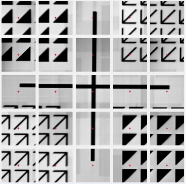
Markets and product roadmap
• Holistic lithography
Driving improvements in EPE
E-beam inspection

                              Public
Our holistic portfolio is more important than ever
                                                                                                                                Slide 7
                                                        Lithography scanner with                                          29 Sept. 2021
                                                       advanced control capability

                                       EUV: NXE and                                  DUV: XT and      Etch and
                                       EXE platforms                                 NXT platforms    deposition tools

       Process window                                                                                Process window
       Prediction and                                                                                Control
       Enhancement

                                                                 Overlay
        Optical proximity correction                               CD                                YieldStar   E-beam

  Computational lithography                                                                          Optical metrology
and computational metrology                                                                          E-beam metrology
                                                                                                     E-beam inspection
                                                                           Process window
                                                                           Detection                                              Public
Our holistic portfolio is more important than ever
                                                                                                                                Slide 8
                                                        Lithography scanner with                                          29 Sept. 2021
                                                       advanced control capability

                                       EUV: NXE and                                  DUV: XT and      Etch and
                                       EXE platforms                                 NXT platforms    deposition tools

       Process window                                                                                Process window
       Prediction and                                                                                Control
       Enhancement

        Optical proximity correction                                                                 YieldStar   E-beam

  Computational lithography                                                                          Optical metrology
and computational metrology                                                                          E-beam metrology
                                                                                                     E-beam inspection
                                                                          Process window
                                                                          Detection                                               Public
Our holistic portfolio is more important than ever
                                                                                                                                Slide 9
                                                        Lithography scanner with                                          29 Sept. 2021
                                                       advanced control capability

                                       EUV: NXE and                                  DUV: XT and      Etch and
                                       EXE platforms                                 NXT platforms    deposition tools

       Process window                                                                                Process window
       Prediction and                                                                                Control
       Enhancement

        Optical proximity correction                                                                 YieldStar   E-beam

  Computational lithography                                                                          Optical metrology
and computational metrology                                                                          E-beam metrology
                                                                                                     E-beam inspection
                                                                          Process window
                                                                          Detection                                               Public
All data available at every step in the flow
Use scanner metrology, YieldStar, HMI metrology and inspection to optimize                                                                               Slide 10
                                                                                                                                                    29 Sept. 2021
sampling for scanner control, and as yield proxy for faster time-to-yield
                                                                                                                           After-etch        After-etch / CMP
  Computational                                         After-litho                                   After-etch
                           Lithography                                            Etch                                      e-beam                e-beam
   lithography                                          metrology                                     metrology
                                                                                                                           metrology            inspection

        Recipe                        Recipe               Recipe                                             Recipe              Recipe           Recipe
 Data                          Data                 Data                             Data              Data                Data             Data

Virtual Computing
Platform                                                                   HMI e-beam HMI e-beam
                       Holistic           Scanner        YieldStar                                   Hybrid Metro
                                                                            Metrology    Inspection
 VCP                 applications        applications   applications
                                                                           applications applications
                                                                                                     applications

                               Single user interface, common features, control framework - through each and every step
                               Shared functions and (domain) models                               Analytics foundation
                                                                                                                                           ASML
                                                                                                         Data infrastructure
                                                                      Equipment and automation integration, security, data solutions

                  Customer generic computing hardware                                                                                      Customer
                                                                                                                                                            Public
Markets and product roadmap
Holistic lithography
• Driving improvements in EPE
E-beam inspection
PublicReducing Edge Placement Error (EPE) is key to improve yield
Local CD errors, due to stochastics, become increasingly important Slide 12
29 Sept. 2021
250 nm
Edge Placement Error (EPE): combined
error of overlay and CD uniformity (global EPE is the best predictor of yield
CDU, local CD errors and OPC error)
CD: Critical Dimension, OPC: Mask Optical Proximity Correction PublicYieldStar overlay metrology – after litho and after etch
Characterizing the process error and enabling accurate feature placement Slide 13
29 Sept. 2021
Optical overlay metrology – after Litho Optical overlay metrology – after Etch
Litho Etch
YS385 YS1385
Metrology Metrology
Accurate overlay data Accurate overlay data
on targets on actual device
Corrections
~800 Points x 4 wafers ~10,000 Points x 2 wafers
Every lot Every few days
Litho overlay control: after Litho sparse + after Etch refine
PublicDriving improvements in EPE
Requires high fidelity, fast and accurate metrology to maximize the Slide 14
29 Sept. 2021
scanner’s correction capabilities
Metrology Monitoring Control
Overlay
YieldStar Layer B to Layer A
Final Dual Layer EPE
Pattern
as designed
>1,000 measurements/wafer 10 million measurements/wafer 60 min
Single layer EPE
Layer B
Wafer HMI ePx Computational EPE
Signature Control Software
>10 million measurements/wafer 60 min
PublicASML scanners to improve EPE and yield
ASML scanners are uniquely able to find, measure and correct for Slide 15
29 Sept. 2021
patterning variations
FlexRay illuminator
Even Fingers
Dose
Odd Fingers
Grey Filter
Optical Centerline
manipulator Y
X
Z
Reticle stage
Metrology stage Exposure stage
100% of wafers 100% of wafers are
are measured processed field-by-field
Wafer stage
Scanner actuators correct
on a field-by-field basis
PublicTighter EPE requirements drive increased metrology
ASML provides accurate, cost-effective overlay, EPE, and defect metrology Slide 16
29 Sept. 2021
Measurements per lot
Overlay EPE Defects
Billions
EPE Requirement
14
Millions
Measurements per lot
12
EPE requirement [nm]
10
Thousands
8
6
4
2015 2018 2021 2024 2027 2030
2
0 Overlay
2015 2018 2021 2024 2027 2030
EPE
Defect Inspection
PublicNeed for part per billion control strategy
Defect-aware monitoring and control in the age of EUV stochastics Slide 17
29 Sept. 2021
Today, server chips can be ~800mm2
in size
PublicNeed for part per billion control strategy
Defect-aware monitoring and control in the age of EUV stochastics Slide 18
29 Sept. 2021
Missing contact hole:
Finding defect in a haystack
1 mm
1 mm
There can be >100M contact holes
per mm2 and increasing by 1.5x per node
Today, server chips can be ~800mm2
in size
PublicNeed for part per billion control strategy
Defect-aware monitoring and control in the age of EUV stochastics Slide 19
29 Sept. 2021
SEM image:
example missing contact hole
so ~80B of these need to function
There can be >100M contact holes
per mm2 and increasing by 1.5x per node
Today, server chips can be ~800mm2
in size
PublicMarkets and product roadmap
Holistic lithography
Driving EPE improvements
• E-beam inspection
PublicHigh resolution E-beam versus Optical bright field inspection
High resolution e-beam provides superior resolution to optical inspection, Slide 21
29 Sept. 2021
enabling detection of tiny pattern fidelity defects
Customer design scaling Optical bright field E-beam capable of capturing part per billion
down to 10nm feature size inspection lacks sensitivity pattern fidelity defects with nanometer resolution
Metal layer design Optical bright field image High resolution e-beam image Design-based inspection
Proc. SPIE 9778, Metrology, Inspection, and Process Control for Microlithography, 97780O (21 April 2016) PublicE-beam inspection has inherent resolution advantage
Increasing throughput through increasing parallelism with multibeam Slide 22
29 Sept. 2021
1000000 Min defect size for
2 nm node and below
100000 Optical
Bright Field
Inspection
10000
1000 Gen 3 Multibeam (~2028)
Throughput [mm²/hr]
Increased
100
throughput
enables
10 additional HVM Gen 2 Multibeam (~2024)
applications
1
0.1 Gen 1 Multibeam (2021)
0.01 Scanning
electron
microscope
0.001 image Single e-beam (R&D)
0.0001
60 40 20 10 8 6 4 2 1
Defect size [nm] PublicE-beam inspection: Voltage Contrast (VC) and physical defect
Unique capability of electron beam inspection to find yield limiting defects Slide 23
29 Sept. 2021
VC inspection: detection of interlayer Physical inspection: detection of intralayer
defects causing electric opens and shorts defects such as design and process weak spots
eScan eScan
ePx
• Heavily used in DRAM and 3D NAND • Used in all market segments
• HMI is the technology leader in e-beam inspection
• HMI leadership enabled by high current, charging control, and fast data rates
PublicMultibeam addresses both VC and physical defect inspection
Delivering cost-effective throughput gains at high resolution Slide 24
29 Sept. 2021
VC inspection: detection of interlayer Physical inspection: detection of intralayer
defects causing electric opens and shorts defects such as design and process weak spots
eScan eScan
ePx
P(-1,1) P(0,1) P(1,1)
P(-1,0) P(0,0) P(1,0)
P(-1,-1) P(0,-1) P(1,-1)
eScan eScan
multibeam multibeam
PublicMultibeam leverages ASML core technologies
Increasing e-beam inspection throughput for high-volume manufacturing Slide 25
29 Sept. 2021
P(-1,1) P(0,1) P(1,1)
P(-1,0) P(0,0) P(1,0)
P(-1,-1) P(0,-1) P(1,-1)
Throughput
3 Brion’s computational technology:
• Deep-learning-enabled image
Single beam system quality enhancement
• Design-based defect inspection
2 ASML’s stage technology:
• High speed motion
• High position accuracy Multibeam systems
now shipped and
installed at customers
1 HMI’s Advanced Electron Optics & MEMS
High quality SEM images
with 9 beams scanning simultaneously
PublicMultibeam: current status
Implementing learnings from eScan1000 (3x3) and driving eScan1100 Slide 26
29 Sept. 2021
(5x5) qualification for first shipment expected in Q4 2021
Key messages
• Multibeam technology is challenging
• We experienced some program delays: ended
original development partnership, COVID
• We added additional expertise to the team and
developed new multibeam IP
• We remain confident about multibeam and are
committed to realizing its market potential
Status today
• 3 eScan1000 prototypes (3x3 beams) running and
under assessment at customers
Imaging results from the • System qualification of eScan1100 (5x5 beams)
eScan1100 5x5 multibeam system moving full speed; first shipment expected Q4 2021
PublicApplications products and business opportunity
Key messages Slide 27
29 Sept. 2021
The Applications business is projected to grow at ~20% CAGR with strong
gross margins over the period 2020 through 2025
The Applications product portfolio supports the ASML scanner business,
driven by our unique capability to help customers maximize patterning
performance
• Driving improvements in Edge Placement Error (EPE)
• Delivering leading solutions for optical and e-beam metrology and
inspection
• Integrating ASML’s complete product portfolio into a Holistic Litho solution to
optimize and control the litho process
Primary drivers of growth are the extension of our EPE roadmap:
• New metrology, inspection and control offerings extend the roadmap
• Innovative products combine computational technology, YieldStar overlay
metrology and e-beam metrology
• Hardware and software products support the introduction of EUV into HVM
• New applications of deep learning in both computational litho and defect
inspection drive improved performance
PublicForward Looking Statements
Slide 28
29 Sept. 2021
This presentation contains statements that are forward-looking, including statements with respect to expected industry and business environment trends including
expected growth, outlook and expected financial results, including expected net sales, gross margin, R&D costs, SG&A costs and effective tax rate, annual revenue
opportunity for 2025, financial model for 2025 and assumptions and expected growth rates and drivers, expected growth including growth rates 2020-2025 and 2020-
2030, total addressable market, growth opportunities beyond 2025 and expected annual growth rate in lithography and metrology and inspection systems and expected
annual growth rate in installed base management, expected trends in addressable market up to 2030, expected trends in Logic and Memory revenue opportunities, long
term growth opportunities and outlook, expected trends in demand and demand drivers, expected benefits and performance of systems and applications, semiconductor
end market trends, expected growth in the semiconductor industry including expected demand growth and capital spend in coming years, expected wafer demand
growth and investments in wafer capacity, expected lithography market demand and growth and spend, growth opportunities and drivers, expected trends in EUV and
DUV demand, sales, outlook, roadmaps, opportunities and capacity growth and expected EUV adoption, profitability, availability, productivity and output and estimated
wafer demand and improvement in value, expected trends in the applications business, expected trends in installed base management including expected revenues and
target margins, expected trends and growth opportunity in the applications business, expectations with respect to high-NA, the expectation of increased output capacity,
plans, strategies and strategic priorities and direction, expectation to increase capacity, output and production to meet demand, the expectation that Moore's law will
continue and Moore's law evolution, product, technology and customer roadmaps, and statements and intentions with respect to capital allocation policy, dividends and
share buybacks, including the intention to continue to return significant amounts of cash to shareholders through a combination of share buybacks and growing
annualized dividends and statements with respect to ESG commitment, sustainability strategy, targets, initiatives and milestones. You can generally identify these
statements by the use of words like "may", "will", "could", "should", "project", "believe", "anticipate", "expect", "plan", "estimate", "forecast", "potential", "intend",
"continue", "target", "future", "progress", "goal" and variations of these words or comparable words. These statements are not historical facts, but rather are based on
current expectations, estimates, assumptions and projections about our business and our future financial results and readers should not place undue reliance on them.
Forward-looking statements do not guarantee future performance and involve a number of substantial known and unknown risks and uncertainties. These risks and
uncertainties include, without limitation, economic conditions; product demand and semiconductor equipment industry capacity, worldwide demand and manufacturing
capacity utilization for semiconductors, semiconductor end-market trends, the impact of general economic conditions on consumer confidence and demand for our
customers’ products, performance of our systems, the impact of the COVID-19 outbreak and measures taken to contain it on the global economy and financial markets,
as well as on ASML and its customers and suppliers, and other factors that may impact ASML’s sales and gross margin, including customer demand and ASML’s ability
to obtain supplies for its products, the success of R&D programs and technology advances and the pace of new product development and customer acceptance of and
demand for new products, production capacity and our ability to increase capacity to meet demand, the number and timing of systems ordered, shipped and recognized
in revenue, and the risk of order cancellation or push out, production capacity for our systems including the risk of delays in system production and supply chain
capacity, constraints, shortages and disruptions, trends in the semi-conductor industry, our ability to enforce patents and protect intellectual property rights and the
outcome of intellectual property disputes and litigation, availability of raw materials, critical manufacturing equipment and qualified employees and trends in labor
markets, geopolitical factors, trade environment; import/export and national security regulations and orders and their impact on us, ability to meet sustainability targets,
changes in exchange and tax rates, available liquidity and liquidity requirements, our ability to refinance our indebtedness, available cash and distributable reserves for,
and other factors impacting, dividend payments and share repurchases, results of the share repurchase programs and other risks indicated in the risk factors included in
ASML’s Annual Report on Form 20-F for the year ended December 31, 2020 and other filings with and submissions to the US Securities and Exchange Commission.
These forward-looking statements are made only as of the date of this document. We undertake no obligation to update any forward-looking statements after the date of
this report or to conform such statements to actual results or revised expectations, except as required by law.
PublicPublic
You can also read