"ASIC 2020" - ASIC and ASIC Success Redefined - eSilicon Corporation
←
→
Page content transcription
If your browser does not render page correctly, please read the page content below
“ASIC 2020” – ASIC and ASIC Success Redefined
By Jack Harding, president and CEO, eSilicon
Published by GSA Forum May 2, 2019; used with permission

Introduction
A major shift in the application-specific integrated circuit (ASIC) market has occurred over the past five years. The
forces at play are most evident at the top end of the market, but they will impact the entire customer base and
supply chain over time. It is well-known that Moore’s Law is finally slowing down. The implications of this trend are
driving complexity increases in ASIC design across new dimensions. One can no longer rely on a faster clock to
deliver the next-generation product.

Instead, substantial amounts of integration are happening at the chip and package levels. More memory, more
processors all aimed at increasing throughput through parallelism and dedicated hardware accelerators. The
result is that an ASIC is now typically multiple chips integrated in a complex 2.5D package. This is the new
definition of ASIC.

The consumers of these new ASICs are changing as well. System companies are now leveraging ASIC
technology as the core enabler to bring new products to market. These new products critically rely on the ASIC
to deliver its intended capability and performance at the system level. The requirement to deliver an ASIC’s
performance in the context of the system is the new definition of ASIC success.

We will call this new definition of ASIC and ASIC success collectively “ASIC 2020.” In this piece we will explore
ASIC 2020 trends, what they mean to the customer, the semiconductor ecosystem and the overall semiconductor
industry.

Examples
A couple of examples of what constitutes an ASIC 2020 design would be helpful. The data center is a good
place to start. As more hyperscale data centers come on line from the likes of Google, Amazon, Microsoft and
Facebook, there is a strategic imperative for these facilities to deliver the highest performance and lowest power
in a scalable, flexible manner. This often means specialized hardware accelerators and artificial intelligence (AI)
technology to support the kind of workloads required by the rather diverse customer base.

Famously, Google has led the pack in this arena with their Tensor Processing Unit, or TPU. This device is an ASIC
used to accelerate machine learning workloads. The TPU was first announced in 2016. Since then, there have been
several new generations of the design, including one that is optimized for the cloud. eSilicon has worked on specialized
data center ASICs as well. Figure 1 summarizes one such design that is currently moving into production.

                                        Figure 1. Data center switching ASIC

The current 5G build-out that is occurring worldwide is another place to look for ASIC 2020 designs. The move
from 4G to 5G wireless infrastructure promises to revolutionize the way we communicate and create entire new
markets associated with trends such as internet of things (IoT) and autonomous vehicles. In turn, all the data
generated by these new applications will ultimately be processed in cloud data centers, so these two trends are
indeed linked. For those of you old enough to appreciate the historical reference, think of the move from 4G to
5G as similar to the move from dial-up to broadband communication. This is also an area eSilicon has some
experience in. Figure 2 summarizes a rather large ASIC that we are bringing into production.

                                           Figure 2. 5G infrastructure chip

Technology enablers
When a new trend emerges, the question is often asked, “Why now?” The answer is usually a combination of
consumer expectations, software advances and technology breakthroughs. In the case of ASIC 2020, it’s a
combination of all these forces. One could debate if companies like Google and Facebook caused consumer
expectations to shift, or if they supported a shift that was already underway. Either way, social media and always-
on data access are here to stay.

The software aspects of these changes are actually not all that new. I’ll cover that in the next section. The
hardware-related innovations are very real and actually enable the software to perform, for the first time, at
human-interaction-class speeds. Some of these breakthroughs include:

• Semiconductor process advances: Innovation primarily around FinFET, or 3D transistor structures, leads the
  way here. While this technology is expensive and presents a daunting design rule book, it delivers the requisite
  power and performance to support advanced applications. The possible move from FinFET to gate-all-around
  structures at 5nm and below promises to up the game even more, with extreme ultraviolet lithography (EUV)
  reducing the number of pages in the design rule book.

• 5/3D packaging: The ability to finally integrate multiple devices on a silicon interposer has opened up many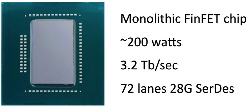
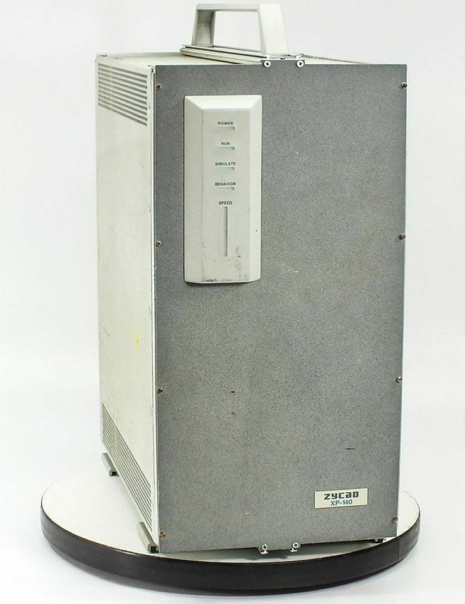
new applications. Most notable these days is the use of multiple high bandwidth memory (HBM) stacks with a
  mission ASIC to facilitate fast access to huge amounts of memory. The HBM standard is evolving to support
  these advances as well. This is just the beginning. 3D promises heterogeneous stacks of purpose-built known-
  good-die from various process technologies. Materials science plays an important role here as well. Watch for
  new technology — organic substrates and even glass interposers.

• Chiplets: The delivery of small, special-purpose silicon slices is another example of 2.5D design that leverages
  packaging technology advances. eSilicon has had some experience with high-bandwidth interconnect devices
  that essentially stitch two chips together to form a larger device.

• Design tools: All of these hardware-based approaches require new forms of design tool support. Thermal and
  mechanical stress analysis now becomes important for advanced packaging. Higher performance puts new
  demands on signal and power integrity. Design rules now have a three-dimensional quality. These are just a few
  of the challenges we face. I am encouraged by the strong R&D efforts being put forth by our electronic design
  automation (EDA) partners in these areas.

History
As mentioned, a lot of the software that is driving ASIC 2020 isn’t new. Neural networks, one of the key drivers for
AI applications, have been around a long time. Do your own Google search and you will find references dating
back to the 1950s. The same timeline applies for machine learning.

There are other contemporary concepts that are not new. Hardware acceleration is one where I can offer some
first-hand experience. Today, hardware accelerators are used to offload special-purpose algorithms, typically
associated with AI, from general-purpose central processing units (CPUs). The idea is that special-purpose
hardware will always produce a more efficient result. If that hardware can be integrated with the overall workload
of the system, there is a win from a performance point of view.

In the 1980s and 1990s, I worked for a company called Zycad. This company built products that performed
logic and fault simulation on special-purpose, dedicated hardware. The goal was to deliver 10X – 1,000X the
performance when compared to state-of-the-art computers running software simulators. In those days, that was
typically a Digital Equipment Corporation VAX computer. It should be no surprise that Zycad was a “hardware
accelerator” company. This was a market niche served by several competitors.

Zycad’s flagship product was the Logic Evaluator. It was the size of a few refrigerators and indeed delivered
simulation performance 10X – 1,000X faster than any general-purpose computer. Zycad also made smaller, desk-
side machines intended for a single user. The XP-140, shaped like a large suitcase was one such product and
Figure 3 illustrates its form factor. (Interestingly, this device is for sale on eBay.)
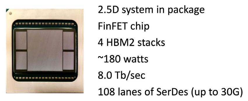
Figure 3. Zycad XP-140 hardware accelerator

Requirements for ASIC 2020
I’ll conclude with an assessment of what’s needed to drive this new ASIC market and the new definition of ASIC
success forward.

• Methodology: A robust chip design methodology is now the entry point, not the end point. The effects of the
  package and system on the chip must now be considered and analyzed very early in the process if fatal errors
  are to be avoided. Chip/package/system design is the new bar and design for manufacturing, design for test,
  signal integrity and power integrity (DFM/DFT/SI/PI) are some of the buzz terms.

• IP platforms: Best-in-class semiconductor intellectual property (IP) is also merely an entry point for ASIC
  2020. Beyond quality and robustness, the collection of IP used in an advanced design must be verified to work
  together. Integration issues such as metal stack compatibility, testability and control interfaces all need to be
  worked out ahead of time. The IP must also be customizable relative to its intended use if power, performance
  and area (PPA) targets are to be met in a reasonable time. We refer to this concept as an IP platform.

• Pre-verified architecture: Beyond IP platforms, look to your ASIC vendor to provide pre-verified, hardened
  architectures of how IP can be integrated to solve a particular problem. This concept dramatically reduces
  integration risks and design time. We call our version of this the ASIC Chassis.

• Materials expertise: It’s not just about silicon for ASIC 2020. Previously mentioned organic and glass
  interposers are in the mix and your ASIC vendor needs to understand the implications.

• Compute infrastructure: The compute resources required for an ASIC 2020 design can be substantial. The
  requirements expand and contract throughout the design cycle and the ability to deploy the most advanced
  compute technology is often the margin of victory. All this demands a cloud-based, scalable architecture.

• A collaborative ecosystem: Perhaps the most important requirement is the ecosystem supporting the overall
  design project. Advanced designs do not come up smoothly. These designs contain many new technologies and
  many, many interdependencies. Recall the new definition of ASIC success — deliver an ASIC’s performance
  in the context of the system. Getting that done takes strong problem-solving skills and relentless collaboration
  across a well-integrated, system-centric ecosystem. All the members of that ecosystem are invested in the
  customer’s success. It simply can’t be done any other way.
Final thoughts
eSilicon has spent the last four years developing all the IP, skills and methodology to supply ASIC 2020 class
devices. The result is a reliable and predictable source that understands the new definition of ASIC and ASIC
success. It’s not your father’s ASIC. We can explain why.

To learn more about eSilicon’s ASIC and IP capabilities, visit https://www.esilicon.com.

                  Jack Harding, co-founder, president and CEO of eSilicon Corporation, is responsible for
                  eSilicon’s overall leadership, strategy and management. Mr. Harding brings more than 30
                  years of management experience in the semiconductor industry, spanning the electronic
                  design automation (EDA) and IC sectors. Prior to co-founding eSilicon in 2000, Mr. Harding
                  was the president and CEO of Cadence Design Systems. Mr. Harding entered Cadence upon
                  the acquisition of Cooper & Chyan Technology (CCT), where he served as the president
                  and CEO and was responsible for leading the company to an IPO. Prior to CCT, Mr. Harding
                  served as the executive vice president of Zycad Corporation. Mr. Harding began his career
                  with distinction at IBM. Mr. Harding currently serves on the board of directors of Qorvo
(previously RF Micro Devices) and the Global Semiconductor Alliance (GSA). He also serves on the GSA Finance
Committee. Mr. Harding holds a Bachelor of Arts in Chemistry and Economics from Drew University and attended
the Stern School of Business at New York University.
You can also read