Designs of Communication Circuits for Side-by-Side and Stacked Chiplets - ISSCC 2021 Forums
←
→
Page content transcription
If your browser does not render page correctly, please read the page content below
ISSCC 2021 Forums

        Designs of Communication Circuits
      for Side-by-Side and Stacked Chiplets

               Kenny Cheng-Hsiang Hsieh

                TSMC, Hsinchu, Taiwan
                   January 2021

©2021 TSMC             ISSCC 2021 Forum       1 of 56

                                                Security C - TSMC Secret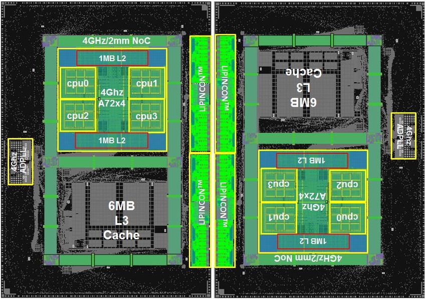
Self Introduction

Kenny C. H. Hsieh is a Director in Design Technology Platform, or DTP, of
TSMC, where he joined in 2012. He currently leads a few mixed-signal
design groups. Most of these groups are based in Hsinchu, Taiwan.

Mr. Hsieh received his BSEE degree from National Cheng Kung University,
Tainan, Taiwan, and MSEE degree from National Chiao Tung University,
Hsinchu, Taiwan, in 1985 and 1989 respectively. He designed SRAM and
DRAM circuits at Winbond and Etron for 6 years, prior to spending several
years at the University of California, Irvine, doing PLL and Gm-C filter
researches. In 1997 to 2012, he designed high-speed transceivers for Ohm
Technology, LSI/Avago, and Xilinx in California.

His current research interests include equalization theory for digital
communication and design/technology co-optimization of advanced
CMOS technologies.
 ©2021 TSMC                                 ISSCC 2021 Forum                2 of 56

                                                                              Security C - TSMC Secret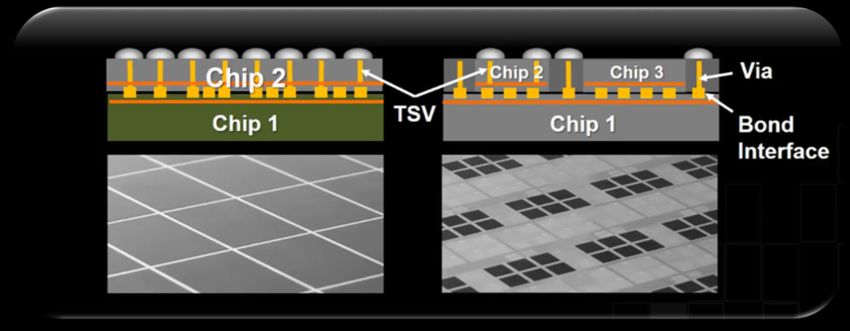
Outline
Backgrounds
Advance Package Technology Overview
Inter-Chiplet Interconnect Design
Design Example Deep-Dive
Conclusions
©2021 TSMC ISSCC 2021 Forum 3 of 56
Security C - TSMC Secret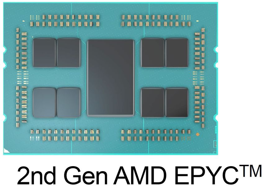
Background
Yield/Die-Area (%/mm2 ) Yields go down for larger chips
2.4X Chiplets to the rescue!
2.1X
Heterogeneous opportunities
1.6X Interposer is the new PC board
1X
Monolithic 2-Chiplet 3-Chiplet 4-Chiplet
Chip Design Design Design
©2021 TSMC ISSCC 2021 Forum 4 of 56
Security C - TSMC Secret
SiP Example-1: MCM Packages
14nm IO-Die
7nm Core-Complex-Die, 8 copies
Infinity Fabric On-Package Links
* S. Naffziger et al., AMD [1]
©2021 TSMC ISSCC 2021 Forum 5 of 56
Security C - TSMC Secret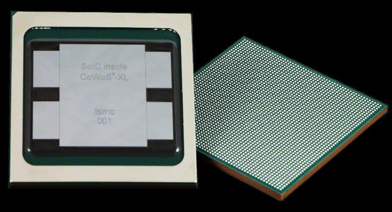
SiP Example-2: Si-Interposers
7nm 4*ARM Cortex-A72 + 6MB Interposer
L3 cache in single chiplet
Symmetric architecture: two
identical chiplets integrated on Si-
Interposer side-by-side
Chiplet 1 Chiplet 2
* M.-S. Lin et al., TSMC [2]
©2021 TSMC ISSCC 2021 Forum 6 of 56
Security C - TSMC Secret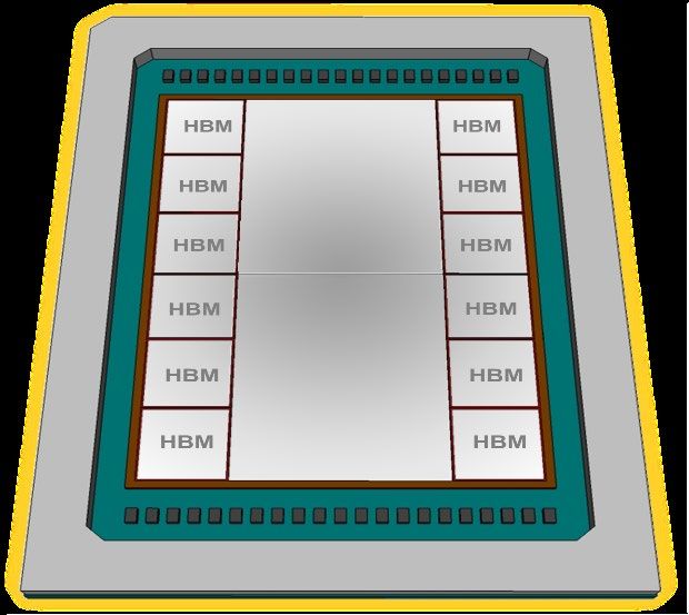
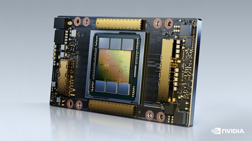
SiP Example-3: 3D (Memory) Stacking
NVIDIA’s A100 80GB GPU with 2TB/s of Memory bandwidth
Six stacks of HBM2E, 3.2Gbps; 5120-bit memory bus
* NVIDIA press release [3]
©2021 TSMC ISSCC 2021 Forum 7 of 56
Security C - TSMC Secret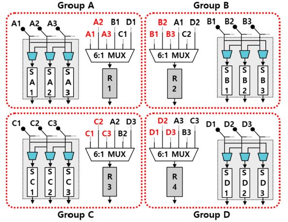
A Short Summary Before We Dive in …
Chiplet SoCs, integrated using 2.5D/3D technologies, opens a
new chapter in chip designs, addition to (slowing) Moore’s law.
Designers need to concurrently consider system requirements,
stacking/package technologies, and interconnect architectures.
Power, area, latency, and transparency to the firmware/software
are the keys.
©2021 TSMC ISSCC 2021 Forum 8 of 56
Security C - TSMC Secret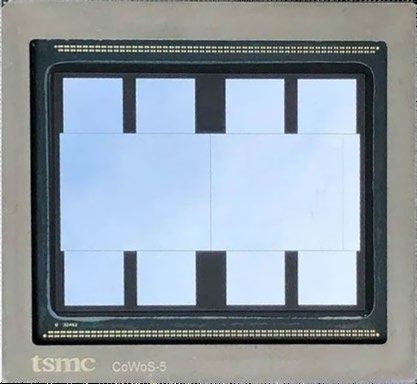
Outline
Background
Advance Package Technology Overview
Inter-Chiplet Interconnect Design
Design Example Deep-Dive
Conclusions
©2021 TSMC ISSCC 2021 Forum 9 of 56
Security C - TSMC Secret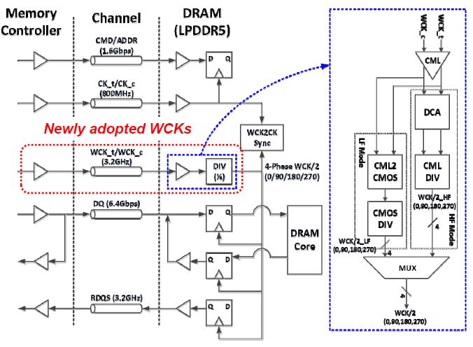
TSMC Wafer Level System Integration Technology
Enable System Level Innovations
Chip Stacking- Frontend 3D Advanced Packaging-
TM
Backend 3D
TSMC-SoICTM 3DFabric CoWoS® InFO
CoW / WoW
SoIC: System on Integrated Chips
CoW: Chip on Wafer CoWoS: Chip on Wafer on Substrate
WoW: Wafer on Wafer InFO: Integrated Fan-Out
©2021 TSMC ISSCC 2021 Forum 10 of 56
Security C - TSMC SecretTSMC 3DFabric TM
Chip Stacking (FE 3D) Advanced Packaging (BE 3D)
InFO-R RDL Interconnect
InFO
InFO
CoW Chip on Wafer (Chip First)
InFO-L LSI + RDL Interconnect
TSMC-
TSMC-
CoWoS®-S Si Interposer
SoICTM
SoIC TM
WoW Wafer on Wafer CoWoS
CoWoS CoWoS®-R RDL Interposer
(Chip Last)
CoWoS®-L LSI + RDL Interposer
SoIC: System on Integrated Chips InFO: Integrated Fan-Out
CoWoS: Chip on Wafer on Substrate
RDL: Redistribution Layer
LSI: Local Si Interconnect
©2021 TSMC ISSCC 2021 Forum 11 of 56
Security C - TSMC SecretTSMC-SoIC TM
Bump-less interconnect, Best proximity
Ultra high density vertical interconnect for high bandwidth, high
power efficiency, and enhanced SI/PI
Flexible stacking – F2F/F2B, CoW/WoW, LoL/LoM etc.
©2021 TSMC ISSCC 2021 Forum 12 of 56
Security C - TSMC SecretTSMC-SoIC Design Rules Roadmap
TM
Aggressive SoIC bond pitch shrink roadmap with advanced
technology node
N5
N7/N6 N5 N3
SoIC Bond Pitch 9 μm 6 μm 4.5 μm
TSV Pitch Min. 9 μm 6 μm 4.5 μm
ESD Requirement 10V 5V 3V
Schedule Q4’20 Q2’21 Q1’23
©2021 TSMC ISSCC 2021 Forum 13 of 56
Security C - TSMC SecretInFO-L (LSI) for Ultra-high Bandwidth Chiplet Integration
Integrating SoC chips with high-density Local Si Interconnect
(LSI) and InFO technology
InFO_R InFO_L (i.e. InFO_LSI)
Chip 1 Chip 2
Chip 1 Chip 2
LSI
Substrate Substrate
I/O Pad pitch (µm) 40μm 25μm
RDL W/S (µm) 2/2 (by 3 RDLs of InFO) 0.4/0.4 (by 4 Mzs on LSI)
C4 Bump Pitch (µm) 130μm 90μm
InFO Size, Reticles 2X 1X
©2021 TSMC ISSCC 2021 Forum 14 of 56
Security C - TSMC Secret®
CoWoS -S for High Performance Computing
2023
4x, 12 HBM
2021
3x, 8 HBM
2019
2X, 6 HBM
2016
1.5X, 4 HBM
2011
1.0X
©2021 TSMC ISSCC 2021 Forum 15 of 56
Security C - TSMC Secret®
CoWoS -L For Heterogeneous Integration
Leverage Si bridge and RDL for bandwidth and cost-effectiveness
TSV in LSI (Local Si Interconnect), active & passive chip
integration optional for better performance, power integrity, and
design flexibility
HBM HBM HBM ASIC
ASIC LSI
HBM HBM Substrate
©2021 TSMC ISSCC 2021 Forum 16 of 56
Security C - TSMC SecretFE 3D + BE 3D Integration – TSMC-SoIC + InFO for Mobile
TM
DRAM
TSMC-SoIC
PCB
©2021 TSMC ISSCC 2021 Forum 17 of 56
Security C - TSMC SecretFE 3D + BE 3D Integration – TSMC-SoIC + CoWoS for HPCTM ®
TSMC-SoIC
Chip-1
Chip-2
Interposer
Substrate
©2021 TSMC ISSCC 2021 Forum 18 of 56
Security C - TSMC SecretOutline
Background
Advance Package Technology Overview
Inter-Chiplet Interconnect Design
Design Example Deep-Dive
Conclusions
©2021 TSMC ISSCC 2021 Forum 19 of 56
Security C - TSMC SecretBump Pitches on MCM, CoWoS/InFO, and SoIC
Bump pitch determines (almost) everything
Circuit complexity, maximum trace length, power/area
efficiencies… all set by the bump pitch
MCM CoWoS/InFO SoIC
Bump Pitch ~130μm 30~40μmWhy Parallel Bus with Forwarded Clock?
Lane-by-lane CDR unnecessary for 2.5D/3D interconnects
Wavelength at 1GHz is about 15cm
½ * 3x10⁸ meter/sec * 10-9 sec = 15 cm
No need to consider termination if travel distance is much less 0.5cm
Single-ended, un-terminated designs are good enough for inter-
chiplet interconnects
People use a forwarded clock, shared by a parallel bus of data
Short trace length ensures matched delays between clock and data
Lane-by-lane CDR wastes too much
©2021 TSMC ISSCC 2021 Forum 21 of 56
Security C - TSMC SecretInterconnect Routing Examples
CoWoS InFO
Coplanar Waveguide (CPWG) Microstrip Line
G-S-G-S-G S-S-S-S
With Ground shielding underneath Wider signal trace width
G
S S
G
S S
G
S S
G
S S
G
©2021 TSMC ISSCC 2021 Forum 22 of 56
Security C - TSMC SecretChannel Characteristics (CoWoS, InFO)
Trace length: ~1mm
CoWoS routing style: InFO routing style:
Coplanar Waveguide (CPWG) Microstrip Line
0
Insertion Loss 0
Crosstalk
-2 CoWoS
-4 -10 InFO
dB(S(12,11))
-6
dB(S(18,14))
dB(S(2,1))
dB(S(7,2))
-8 -20
-10
-12 -30
-14
-16
CoWoS
-40
-18
InFO
-20 -50
0 2 4 6 8 10 12 14 16 18 20 0 2 4 6 8 10 12 14 16 18 20
Frequency (GHz) Frequency (GHz)
©2021 TSMC ISSCC 2021 Forum 23 of 56
Security C - TSMC Secret2.5D Die-to-Die Routing Considerations
Number of row in depth
Deeper rows
Longer trace length
Better beachfront density
Poor power delivery
Lower data rate per pin
Number of layers in RDL
More layer
Higher cost
Better crosstalk from
shielding/decoupling
Width per routing wire
Wider trace
Lower impedance
Lower insertion loss
All in variant matrix!
©2021 TSMC ISSCC 2021 Forum 24 of 56
Security C - TSMC Secret3D Die-to-Die Routing Considerations
Loading from horizontal interconnect is replaced with cascaded
TSV in multi-dies stacking
Across-chiplet LVS verification is another challenge
A Die-1
A’
Die-2
TSV
Die-3
Die-4
©2021 TSMC ISSCC 2021 Forum 25 of 56
Security C - TSMC SecretChiplet-to-Chiplet Clock Schemes – Two Primaries
Clock sources from both sides (symmetric)
Same crystal oscillator (No PPM difference)
PLL PLL
* P. Vivet et al., CEA-LETI-MINATEC [2]
©2021 TSMC ISSCC 2021 Forum 26 of 56
Security C - TSMC SecretChiplet-to-Chiplet Clock Schemes –Primary/Secondary
DRAM die uses clock from SoC die
System Clock: Phase
one copy Adjustment
PLL
Cluster Clock:
many copies
* C.-K. Lee et al., Samsung [4]
©2021 TSMC ISSCC 2021 Forum 27 of 56
Security C - TSMC SecretStory of “ESD Inside a Package”
No need for HBM protection, CDM substantially reduced
Less loading from ESD lower area & power
MCM CoWoS/InFO SoIC
ESD CDM
High Medium Low
Target
ESD
Capacitance High Medium Low
Load
Efficiency Low Medium High
©2021 TSMC ISSCC 2021 Forum 28 of 56
Security C - TSMC SecretSimultaneously Switching Noise Concerns
High speed (>1Gbps), wide parallel bus (>100-pin)
applications
The interconnect IO is less power hungry due to
Lower ESD load
Shorter trace length
Lower driving of interconnect IO
Even lower power from low-swing
©2021 TSMC ISSCC 2021 Forum 29 of 56
Security C - TSMC SecretSimultaneously Switching Noise Design Solutions
PVT calibration for IO driving strength
Data-Bus-Inversion (DBI): reduce data toggling rate to
less than 50%
Require additional pin in interconnect along with data-bus
Wider data-bus share the DBI coding
larger XOR delay
better interconnect efficiency
Dedicated power domain for I/O driver; either from on-
die LDO or from power bumps
©2021 TSMC ISSCC 2021 Forum 30 of 56
Security C - TSMC SecretSimultaneously Switching Noise Design Solutions
De-coupling capacitance: reduce power bouncing
Reserve De-coupling Cap. around I/O into dense floorplan
Ex: 1:1 area of I/O to De-coupling Cap.
De-coupling Cap.
Each I/O
©2021 TSMC ISSCC 2021 Forum 31 of 56
Security C - TSMC SecretRedundancy and Repair
To improve the yield of the stacking samples
Leverage boundary-scan test to identify the bad lane
The more redundant lanes
the higher repairment-rates
the less interconnect density
©2021 TSMC ISSCC 2021 Forum 32 of 56
Security C - TSMC SecretVarious Lane Redundancy Schemes
RTSV STSV
Switching
Repair
Ring Based 2019 New Proposal
Repair (Shift and Switching Repair)
Shifting
Repair
* I. Lee et al., Yonsei University, Seoul, South Korea[8]
©2021 TSMC ISSCC 2021 Forum 33 of 56
Security C - TSMC SecretTerminologies in 2.5D/3D Production
Example: CoWoS ENG & Production Test Flow
Chip
eDRAM1
Wafer * M.-S. Lin et al., TSMC [10]
uBump Chip1
process
SOC
Chip 2
Wafer Stack on C4
uBump Chip2 Die Sil-to-Sub
process Sil Bump
Si-
Interposer
Probe PAD C4 probe Socket
CP test CP test Package
Test
KGD KGS
(Known-Good-Die) (Known-Good-Stack)
©2021 TSMC ISSCC 2021 Forum 34 of 56
Security C - TSMC SecretBuilt-in Testability in 2.5D/3D Testing Flows
KGD (Known-Good-Die)
DFT-DC, DFT-AC, Boundary scan TAP BIST
At-speed loopback BIST
Loopback eye scan characterization
KGS (Known-Good-Stack)
Interconnect-IO boundary scan for quick defect
screen on interconnect
Cross die at-speed BIST
Eye scan characterization on interconnect
©2021 TSMC ISSCC 2021 Forum 35 of 56
Security C - TSMC SecretBump Pitch (
Shmoo of Link vs. TX Swing
8Gb/s/pin; 320-bit bus toggling (0.6V to 0.1V TX Swing)
9.6Gb/s
8.8Gb/s
8.0Gb/s
7.2Gb/s
6.4Gb/s
5.6Gb/s
4.8Gb/s
0.0V 0.1V 0.2V 0.3V 0.4V 0.5V 0.6V
* M.-S. Lin et al., TSMC [2]
©2021 TSMC ISSCC 2021 Forum 37 of 56
Security C - TSMC SecretWhat’s the Key Parameter Index?
Chiplet partition should be transparent to firmware and software
KPI
CoWoS Remark
SoIC
/InFO
1. Maximize data rate based on bump
Data Rate limited situation.
per pin 1~20 2. Higher data rate under longer trace,
(Gbps) requires more circuit techniques;
degrades the energy efficiency.
1. Expanding upon system request.
Bus Width To be Scalable 2. Modular design concept.
3. Granularity for flexible usage.
©2021 TSMC ISSCC 2021 Forum 38 of 56
Security C - TSMC SecretWhat’s the Key Parameter Index?
KPI
CoWoS Remark
SoIC
/InFO
Aggregate
1. Data-Rate-per-pin*Bus-Width.
Bandwidth 50~500
2. Total computing power.
(GBps)
1. Normalize with aggregate bandwidth.
2. Consider power from I/O, Serialize/De-
Energy
serialize logic, clock distribution, and
Efficiency 0.2~0.5 0.1~0.2
some logic features specific for
(pJ/bit)
interconnect:
ex: DBI, repair support.
©2021 TSMC ISSCC 2021 Forum 39 of 56
Security C - TSMC SecretWhat’s the Key Parameter Index?
KPI
CoWoS Remark
SoIC
/InFO
Beachfront
1. More rows of interconnect bumps; longer
Efficiency 0.5~2 NA
trace; more RDL layers; higher cost.
(Tbps/mm)
Area 1. Bump pitch determines everything.
Efficiency 1~20 10~50 2. Maximize efficiency based on bump
(Tbps/mm2) limited situation.
Latency 1. Function dependent. Ex: Serialize/De-
~4
(T) serialize-ratio, FIFO, DBI, Repair, etc.
©2021 TSMC ISSCC 2021 Forum 40 of 56
Security C - TSMC SecretOutline
Background
Advance Package Technology Overview
Inter-Chiplet Interconnect Design
Design Example Deep-Dive
“A 7nm 4GHz ARM®-Core-Based CoWoS® Chiplet Design
for High Performance Computing” [2]
Conclusions
©2021 TSMC ISSCC 2021 Forum 41 of 56
Security C - TSMC Secret320GB/s on CoWoS for HPC
Symmetric architecture Interposer
Four ARM Cortex-A72 + 6MB L3
cache in single chiplet
Two identical chiplets (KGD)
side-by-side integrate on
interposer
Chiplet 1 Chiplet 2
©2021 TSMC ISSCC 2021 Forum 42 of 56
Security C - TSMC SecretSlim and Side-by-Side Interconnect
One CH for CPU
CPU Channel (Master)
One CH for L3 cache Sub-Channel[3:0] TX_DQ[19:0]
8Gb/s/pin, 160-TX/160-RX pins
TX_DBI
VDDQ=0.3V
TX_VLD
IO RX_DQ[19:0]
(20+2) RX_DBI
Interposer RX_VLD
RX
FIFO
IO
(20+2)
VDDQ=0.3V TX_DQS_t/c
PD
SOC’s AC- IO
CLK couple
AC- DLL RX_DQS_t/c
DLL ESD couple (R90)
(Deskew) (CDM) IO
ADPLL
Chiplet 1 Chiplet 2 L3 Channel (Slave)
©2021 TSMC ISSCC 2021 Forum 43 of 56
Security C - TSMC SecretSlim and Side-by-Side Interconnect in Floorplan
Per Channel: Modularized Sub-channel
400um(W)*2400um(H) 20-bit TX-DQ / 20-bit RX-DQ
Two DLLs built-in
Easy for bandwidth scaling
PLL
Bump Plan
Clock Distribution (4GHz) Signals
Power/Gnd
H: 2400um
W: 400um
©2021 TSMC ISSCC 2021 Forum 44 of 56
Security C - TSMC SecretWhat Are Inside the Boxes?
Dedicated PLL CPU Channel (Master)
Sub-Channel[3:0] TX_DQ[19:0]
TX_DBI
VDDQ=0.3V
TX_VLD
IO RX_DQ[19:0]
(20+2) RX_DBI
RX_VLD
RX
FIFO
IO
(20+2)
VDDQ=0.3V TX_DQS_t/c
PD
SOC’s AC- IO
CLK couple
AC- DLL RX_DQS_t/c
DLL ESD couple (R90)
(Deskew) (CDM) IO
ADPLL
L3 Channel (Slave)
©2021 TSMC ISSCC 2021 Forum 45 of 56
Security C - TSMC SecretWhat Are Inside the Boxes?
Dedicated PLL CPU Channel (Master)
De-skew DLLs Sub-Channel[3:0] TX_DQ[19:0]
TX_DBI
VDDQ=0.3V
TX_VLD
To align between SoC and PHY-TX
IO RX_DQ[19:0]
(20+2) RX_DBI
RX_VLD
RX
FIFO
IO
(20+2)
VDDQ=0.3V TX_DQS_t/c
PD
SOC’s AC- IO
CLK couple
AC- DLL RX_DQS_t/c
DLL ESD couple (R90)
(Deskew) (CDM) IO
ADPLL
L3 Channel (Slave)
©2021 TSMC ISSCC 2021 Forum 46 of 56
Security C - TSMC SecretWhat Are Inside the Boxes?
Dedicated PLL CPU Channel (Master)
De-skew DLLs Sub-Channel[3:0] TX_DQ[19:0]
TX_DBI
VDDQ=0.3V
TX_VLD
To align between SoC and PHY-TX
IO RX_DQ[19:0]
Setup/Hold time auto-centering at (20+2) RX_DBI
cross die interface RX
RX_VLD
FIFO 8Gb/s
IO
(20+2)
VDDQ=0.3V TX_DQS_t/c
PD
SOC’s AC- IO
CLK couple
AC- DLL RX_DQS_t/c
DLL ESD couple (R90)
(Deskew) (CDM) IO
ADPLL
L3 Channel (Slave)
©2021 TSMC ISSCC 2021 Forum 47 of 56
Security C - TSMC SecretWhat Are Inside the Boxes?
Dedicated PLL CPU Channel (Master)
De-skew DLLs Sub-Channel[3:0] TX_DQ[19:0]
TX_DBI
VDDQ=0.3V
TX_VLD
To align between SoC and PHY-TX
IO RX_DQ[19:0]
Setup/Hold time auto-centering at (20+2) RX_DBI
cross die interface RX
RX_VLD
RX FIFO
FIFO
IO
(20+2)
To tolerate phase drift from clock- VDDQ=0.3V TX_DQS_t/c
trees power supply noises and SOC’s
PD
AC- IO
temperature variation CLK couple
AC- DLL RX_DQS_t/c
DLL ESD couple (R90)
(Deskew) (CDM) IO
ADPLL
L3 Channel (Slave)
©2021 TSMC ISSCC 2021 Forum 48 of 56
Security C - TSMC SecretDLL Architecture for Easily Scaling
Two-step DLL FOUT
1st loop: lock clock FBK
2nd Loop
period and divide into PI[15:0]
PD2 VDD VDD
8-phases 2 FREF
2nd loop: interpolate 16 8
... ...
DCDL
sub-phases
IN1 IN2
FOUT90 OUT
... ...
Require only one clock FIN FOUT360
phase VSS VSS
PD1
Easy scaling & with
wide coverage range
1st Loop 90°
135° 45°
0° 225° 90° 315° 180°
2ps
S2D 180° 0°
180° 45° 270° 135° 360° 225° 315°
270°
©2021 TSMC ISSCC 2021 Forum 49 of 56
Security C - TSMC SecretDLL Architecture for Easily Scaling
Two-step DLL
Leverage DLL module for two purposes (Deskew & R90)
DLL-Deskew DLL-R90
SOC/CPU’s clock tree IO-RX’s clock tree
FOUT FOUT
FBK FBK
PI[15:0] PI[15:0]
PD2 PD2
2 FREF 2 FREF
(from SOC/CPU)
DCDL 8 DCDL 8
FOUT90 FOUT90
FOUT360 FOUT360
FIN FIN
(from PLL) (from PLL)
PD1 PD1
©2021 TSMC ISSCC 2021 Forum 50 of 56
Security C - TSMC SecretRiver Routing on CoWoS
Matched routing pattern (dummy rows on top and bottom)
Trace length: 500μm
Die-A Die-B (R180)
80um
RX[0] RX[1] TX[1] TX[0] DMY DMY DMY DMY
TX[0] TX[1] RX[1] RX[0]
Probe PAD Microbump
... 500um trace length ... 40um
DMY DMY DMY DMY
©2021 TSMC ISSCC 2021 Forum 51 of 56
Security C - TSMC SecretPower Consumption
320GB/s aggregate
bandwidth
8Gb/s/pin
0.073pJ/bit ‘IO’
energy efficiency
0.56pJ/bit ‘PHY’
energy efficiency
©2021 TSMC ISSCC 2021 Forum 52 of 56
Security C - TSMC SecretSummary of Key Parameter Index
KPI Design
Examples
CoWoS/InFO SoIC CoWoS’19
Data Rate per pin
1~20 8
(Gbps)
Aggregate Bandwidth
50~500 320
(GBps)
Energy Efficiency
0.2~0.6 0.1~0.2 0.56
(pJ/bit)
Beachfront Efficiency
0.5~2 NA 0.67
(Tbps/mm)
Area Efficiency
1~20 10~50 1.6
(Tbps/mm2)
©2021 TSMC ISSCC 2021 Forum 53 of 56
Security C - TSMC SecretConclusions
Game changer of 3D-stack SoIC with bond pitch scaling down to
4.5um is achievable in coming years
From MCM (130um) to CoWoS/InFO (40um) to SoIC (4.5um)
Design perspective changes throughout and
innovation/opportunity everywhere
Need to co-optimize factors of systems, technologies, circuits to
get them right.
©2021 TSMC ISSCC 2021 Forum 54 of 56
Security C - TSMC SecretAcknowledgments
Mu-Shan Lin Kevin Wu
Chien-Chun Tsai Abraham Tao
Alvin Loke Michael Ming-Tsun Lin
Wen-Hung Huang Joe Wang
Yu-Chi Chen Tze-Chiang Huang
Shu-Chun Yang Mei Wong
Tzu-Heng Chang Stefan Rusu
Mark Chen Frank Lee
©2021 TSMC ISSCC 2021 Forum 55 of 56
Security C - TSMC SecretReferences
[1] S. Naffziger et al., “AMD Chiplet Architecture for High-Performance Server and Desktop Products,” in IEEE ISSCC,
San Francisco, CA, Feb. 2020
[2] M.-S. Lin et al., “A 7nm 4GHz Arm®-core-based CoWoS® Chiplet Design for High Performance Computing,” in
IEEE Symp. VLSI Technology, Tokyo, Japan, Jun. 2019
[3] NVIDIA Doubles Down: Announces A100 80GB GPU, Supercharging World’s Most Powerful GPU for AI
Supercomputing (https://nvidianews.nvidia.com/news/nvidia-doubles-down-announces-a100-80gb-gpu-
supercharging-worlds-most-powerful-gpu-for-ai-supercomputing)
[4] C.-K. Lee et al., “A 7.5Gb/s/pin LPDDR5 SDRAM with WCK Clocking and Non-Target ODT for High Speed and with
DVFS, Internal Data Copy, and Deep-Sleep Mode for Low Power,” in IEEE ISSCC, San Francisco, CA, Feb. 2019
[5] JESD8-28 “300mV interface”
[6] M.-S. Lin et al., “A 16nm 256-bit Wide 89.6GByte/s Total Bandwidth In-Package Interconnect with 0.3V Swing
and 0.062pJ/bit Power in InFO Package,” in HotChips, Stanford, CA, Aug. 2016
[7] R. Venkatesan et al., “A 0.11 PJ/OP, 0.32-128 Tops, Scalable Multi-Chip-Module-Based Deep Neural Network
Accelerator Designed with A High-Productivity vlsi Methodology,” in HotChips, Stanford, CA, Aug. 2019
[8] I. Lee et al., “Highly Reliable Redundant TSV Architecture for Clustered Faults,” in IEEE TRANSACTIONS ON
RELIABILITY, Mar. 2019
[9] S. Khushu et al., “Lakefield: Hybrid cores in 3D Package,” in HotChips, Stanford, CA, Aug. 2019
[10] M.-S. Lin et al., “An extra low-power 1Tbit/s bandwidth PLL/DLL-less eDRAM PHY using 0.3V low-swing IO for
2.5D CoWoS application,” in IEEE Symp. VLSI Technology, Tokyo, Japan, Jun. 2013
©2021 TSMC ISSCC 2021 Forum 56 of 56
Security C - TSMC SecretYou can also read