Integrated spiral waveguide amplifiers on erbium-doped thin-film lithium niobate
←
→
Page content transcription
If your browser does not render page correctly, please read the page content below
Integrated spiral waveguide amplifiers on erbium-doped thin-film lithium
niobate
Xiongshuo Yan∗ ,1 Yi’an Liu∗ ,1 Jiangwei Wu,1 Yuping Chen,1, a) and Xianfeng Chen1, b)
State Key Laboratory of Advanced Optical Communication Systems and Networks,
School of Physics and Astronomy, Shanghai Jiao Tong University, Shanghai 200240,
China
(Dated: 4 May 2021)
Integrated optical amplifiers and light sources are of great significance for photonic integrated circuits (PICs)
and have attracted many research interests. Doping rare-earth ions in materials as a solution to realize
arXiv:2105.00214v1 [physics.optics] 1 May 2021
efficient optical amplifiers and lasing has been investigated a lot. We investigate the erbium-doped lithium
niobate on insulator (LNOI). Here, spiral waveguide amplifiers were fabricated on a 1-mol% erbium-doped
LNOI by CMOS-compatible technique. We demonstrated a maximum internal net gain of 8.3 dB at 1530 nm
indicating a net gain per unit length of 15.6 dB/cm with a compact spiral waveguide of 5.3 mm length and
∼0.06 mm2 footprint. The erbium-doped integrated lithium niobate spiral waveguide amplifiers would pave
the way in the PICs of the lithium niobate platform, especially in achieving efficient integration of active and
passive devices on a lithium niobate thin film, which will make full use of its excellent physical properties
such as remarkable photoacoustic, electro-optic, and piezoelectric characteristics.
Integration is of great significance in device minia- ampilifiers based on the LNOI. It’s worth noting that
turization and improving energy efficiency1 . Photonic a efficient waveguide amplifier based on erbium-doped
integrated circuits as one of important goals for the thin film LN has been realized recently29 . However, this
development of photonics have attracted enormous at- straight waveguide amplifier with a length of 5-mm is
tentions and became one of the most invetigated re- still too long to realize a more compact on-chip photonic
search fields. Lithium niobate (LN) as an emrging in- integration, especially for a chip with a large number of
tegrated photonic platform material is widely used in functional devices.
optical and microwave fields, due to its rich properties Here, we demonstrated a spiral waveguide amplifier
as wide transparent wavelength range, excellent electro- with a maximum net gain of 8.3 dB on a 1-mol% erbium-
optic, acousto-optic characteristics and large second- doped LNOI, with a 15.6 dB/cm net gain per unit length.
order nonlinear susceptibility2 . In particular, with the The spiral waveguide amplifiers with total 5.3-mm-long
lithium niobate on insulator (LNOI) commercializing, and ∼0.06 mm2 of footprint based on the CMOS com-
more compact and low-cost photonic devices with high- patible process, presents strong light confinement for the
performance can be achieved on LNOI, which is very im- signal and pump light and have great significance on pho-
protant for the Photonic integrated circuits, especially for tonic integrated circuits. We shows that it is possible to
the development of a large number of integrated func- achieve efficient on-chip amplifiers with a small footprint
tional devices3–5 . Many on-chip optical devices based spiral waveguides, which would pave the way for the ac-
on LNOI have been demonstrated, such as efficient fre- tive and passive photonic devices integration of various
quency convetors6–10 , electro-optical moudulators11–14 , functionalities on the erbium-doped LNOI platform.
frequency comb source15–17 . However, for a complete The spiral waveguide amplifiers were fabricated on
photonic integrated circuits, integrated waveguide am- a 1-mol % Z-cut erbium-doped LNOI, with 600-nm-
plifiers and light sources are essential elements to realize thick erbium-doped lithium niobate (LN), 2-µm-thick sil-
on-chip various functionalities. Due to the LN is not a ef- ica (SiO2 ) and 500-µm-thick silicon (Si) substrate [Fig.
ficient gain medium, we can not achieve waveguide ampli- 1(a)]. Here, we select the lithium niobate (LiNbO3 ) as
fier and lasing directly on a LNOI. In order to overcome a host materials due to its excellent physical properties
this shortage, the most straightforward approches is to compared to orther materials. In order to obtain uniform
doping rare earth ions into the LNOI, which is similar erboum ions doping concentration and achieve a better
to the erbium doped fiber amplifier. Actually, erbium- gain effect, we doped erbium ions into LN during the
doped laser and waveguide amplifeir have been realized crystal growth processes24.
in many host materials and show great potential for
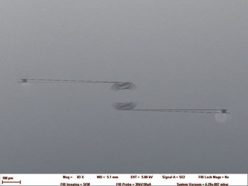
integrated waveguide amplifiers and light sources18–23 . Figure 1(b) shows the scanning electron microscope
The on-chip whispering gallery mode lasers based on (SEM) image of the spiral waveguide amplifier. The to-
the LNOI also have been demonstrated, recently24–28 . tal length of the spiral waveguide amplifier is 5.3 mm
But, there are still less research works about the on-chip with a minimum radius of 25 µm in the bend part of
the spiral waveguides. The footprint of the whole spiral
waveguide is ∼0.06 mm2 , which is the smallest among
all erbium-doped LNOI waveguide amplifiers29–31 , to the
a) Electronic mail: ypchen@sjtu.edu.cn best of our knowledge. Since it will be more suitable for
b) Electronic mail: xfchen@sjtu.edu.cn the compact on-chip integration. Insets in Fig. 1(b) are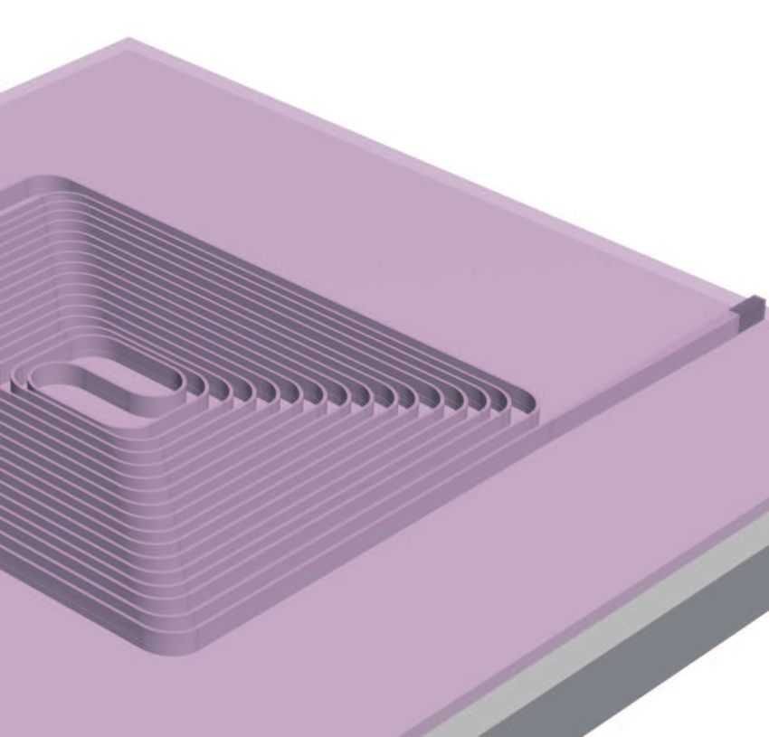
2
(a) (b)
the pump (980 nm) and signal (C-band) wavelength.
~0.06 mm2
Figure (3) shows the experimental setup for the charac-
terization of the sprial waveguide amplifier net gain. The
spiral waveguide amplifier was pumped by two 980-nm
Er:LNOI
2 μm 25 μm laser sources (LR-MFJ-980, actual output wavelength
(c) at 974 nm) from both the input and output sides. A
EBL RIE
continuous-wave (CW) telecom tunable laser (New Fo-
cus TLB-6728, linewidth ¡ 200 kHz, 1520-1570 nm) was
Er:LiNbO3 SiO2 Si substrate α-Si Resist
combined by a wavelength division multiplexer (WDM)
and coupled into the spiral waveguide from one side. The
FIG. 1. Schematic of the spiral waveguide amplifiers and its in-line polarization controllers were used to make the TE
breif fabrication processes. (a) A spiral waveguide amplifier polarization light coupling into the device. Then, the
on a erbium-doped LNOI. (b) Scanning electron microscope output light was collected by a optical spectrum ana-
(SEM) images of the whole spiral waveguide amplifier, and the lyzer (OSA) from the 1550 port of the WDM. The top
magnified coupling grating and spiral waveguide with false- inset shows the photograph of the spiral waveguide am-
color. (c) The brief fabrication processes of spiral waveguide plifier pumped by 974 nm light with strong up-conversion
amplifiers. EBL: electron beam lithography, RIE: reactive ion induced green photoluminescence. The bottom inset in
etching. Fig. 3 shows the optical microscope image of the small
footprint spiral waveguide amplifier comparing with a
TE00 @974nm single-mode optical fiber (Coning SMF-28).
Er:LN
We characterized the propagation losses of the spiral
waveguide amplifier at the signal wavelength (1550 nm)
60°
TE00 @1550nm
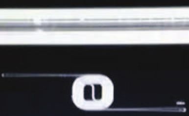
by a microring. Figure (4) shows the SEM image of the
microring with the top width of 1 µm and radius of 30
SiO2 µm, which exhibits the loaded and intrinsic Q factor of
1 μm 5 × 10⁴ and 5.4 × 10⁴ , respectively. We can estimate
the propagation loss α of the spiral waveguide based on
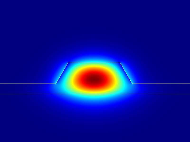
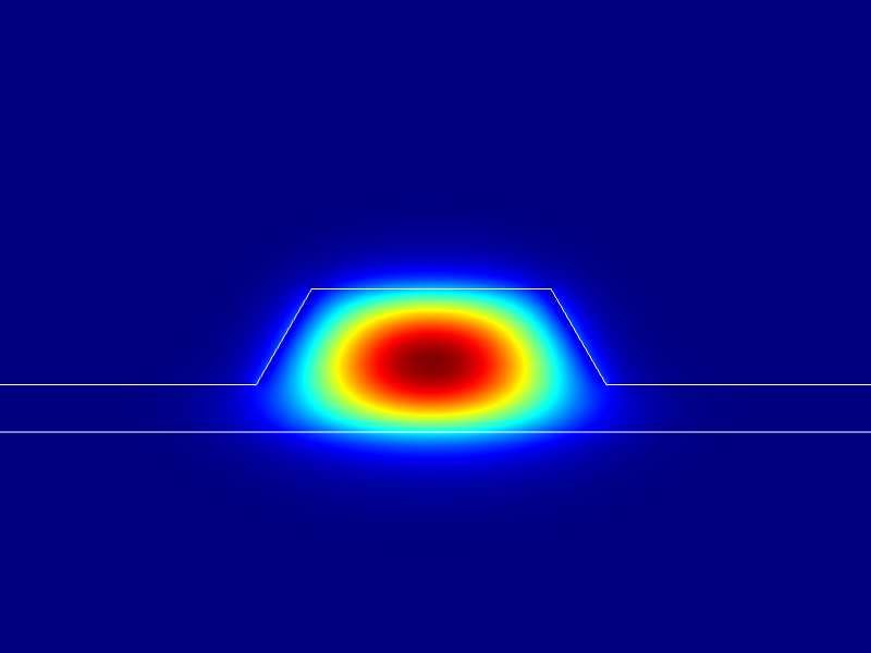
FIG. 2. The false-color SEM image of the fabricated spiral the equation α = 2πnef f /λ0 QI , where nef f is the effec-
waveguide cross-section and simulated electric field distribu- tive index of the waveguide and λ0 is the target wave-
tions of the TE00 modes at 1550 nm and 974 nm. The top length. The calculated propagation loss at 1550 nm is
width of spiral waveguide is 1 µm, with the thickness around ∼ 6.86dB/cm, which lead to a loss about 3.64 dB for
350 nm and a sidewall angle of ∼ 60◦ our 5.3-mm spiral waveguide amplifiers. We also mea-
sured the coupling losess of our coupling grating at 980
nm and 1550 nm, which are 16 dB and 13.4 dB, respec-
the magnified grating and spiral waveguides part SEM tively. The launched pump and signal powers into the
image with false color. In order to obtain high coupling spiral waveguide have been calibrated by using the above
efficiency for pump and signal light. The coupling grat- measurement results.
ing is designed to be two part with periods as 900nm for Figure 5(a) presents the measured signal spectra at
1550 nm (Top, duty cycle 0.33) and 1.05 µm for 980 nm 1530 nm with the increasing pump power, which shows
(bottom, duty cycle 0.46). the apparently signal enhancement. Figrure 5(b) is the
The brief fabrication processes of spiral waveguide am- amplifier net gain as a function of the launched pump
plifiers are shown in Fig. 1 (c). Mainly fabrication details power with different signal powers at 1530 nm. As
including five steps: (1) a 600-nm thick amorphous silicon expected, the spiral waveguide optical gain increases
was deposited as a hard etching mask, (2) a layer of resist rapidly at the small pump powers. Then, we can ob-
was spin-coated onto the Er:LNOI, (3) the spiral waveg- served the gain approaching saturation with the launched
uide structure was patterned via electron-beam lithogra- pump power increasing around 10 mW. A maximum net
phy (EBL), (4) the mask layer patterns was transferred internal gain of 8.3 dB is achieved with the signal power
to the Er:LN layer with an Ar+ plasma etching process at -10.7dBm and pump power at 10.78 mW, which corre-
and (5) the residual mask was removed by wet etching. sponding to a net gain per unit length of ∼ 15.6 dB/cm.
Figure 2 shows the cross sections of the spiral waveg- It is higher than other erbium-doped LNOI29 and bulk
uide (left) and simulated electric field distributions of the LN32,33 . What’s more, a small gain saturation is also
TE00 modes (right) at pump and signal wavelength. The found when the launched signal power increasing, shown
fabricated spiral waveguides have a top width of 1 µm, as Fig. 5(c). The net gain at orther wavelengths of
a thickness of 350-nm, and a sidewall angle of ∼ 60◦ , telecommubication bands is characterized as shown in
shown as the waveguide cross-section SEM image. From Fig. 5(d), with a launched signal power at -10.7 dbm.
the electric field distribution we find that the micron- The pink area of Fig. 5(d) shows the net gain over 3
scale waveguides can support strong light confinement. dB and we can find that the spiral waveguide amplifier
The transverse electric (TE) modes are selected both for exhibits a net gain bandwidth of 1530-1570 nm. These re-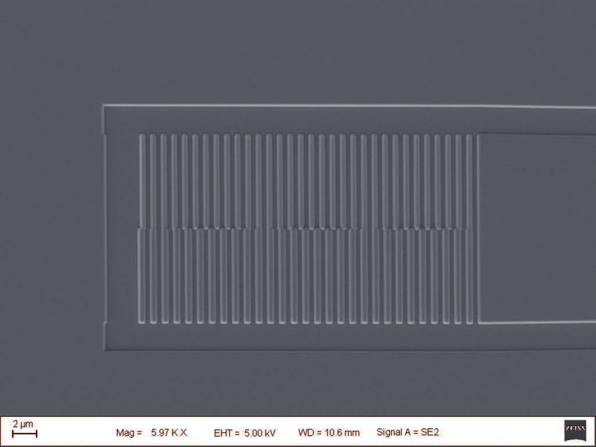
3
974 nm
Pump Laser PC Optical
Spectrum
Analyzer
1550 nm WDM
1550/980 Sample
WDM
1550/980 974 nm
Tunable Laser PC 125 μm PC
Coning SMF-28
Pump Laser
Amplifier
FIG. 3. The net gain measurement setup. Insets are the microscope photograph of the spiral waveguide amplifiers pumped by
974 nm light with strong up-conversion induced green photoluminescence (Top) and the optical microscope image of the spiral
waveguide amplifier comparing with a single-mode optical fiber (Coning SMF-28) (bottom).
(a) (b) (a) (b)
0.22 4 9.0
Q L =5×10
Amplifier net-gain (dB)
4 8.0
Q I =5.4×10
Transmission (a.u.)
0.20 7.0
Signal intensity (a.u.)
16
10.71 6.0
12
Signal @ -10.7dBm
)
8.36
mW
0.18 8 Signal @ -8.7dBm
5.86 5.0 Signal @ -5.1dBm
p(
4
m
0 3.33
Pu
4.0
0.16 1528 1530 1532 2 4 6 8 10 12
Wavelength (nm) Launched pump power (mW)
-40 -20 0 20 40
(c) (d)
Detuning 8.3
10
Amplifier net-gain (dB)
Net internal gain (dB)
8.2
FIG. 4. Propagation loss measurement with a micro-ring. (a) 8
The false-color SEM image of microring with the radius of 30 8.1 6
µm. (b) The Lorenztian fitting exhibiting the microring with 8.0 Signal @1530 nm 4
a loaded Q factor of QL = 5 × 10⁴ and intrinsic Q factor of Pump power @10.78 mW
7.9 2
QI = 5.4 × 10⁴ .
7.8 0
100 150 200 250 300 1520 1530 1540 1550 1560 1570
Launched signal power (μW) Wavelength (nm)
sults show the potential for on-chip integration with high
FIG. 5. Gain characterization of spiral waveguide amplifiers.
optical gain amplifier in erbium-doped LNOI platform. (a) Measured signal spectra as a function of launched pump
In conclusion, we fabricated high-gain optical spiral power at 1530 nm. (b) Measured net internal gain at different
waveguide amplifiers with total 5.3-mm-long and ∼0.06 launched signal powers (1530 nm) as a function of launched
mm2 of areas on a 1-mol% erbium-doped LNOI. A maxi- pump power. (c) Measured net internal gain as a function of
mum internal net gain of 8.3 dB at 1530 nm and a broad launched 1530 nm signal powers with a fixed pump powers
gain band (1530-1570 nm) have been demostrated. A at 10.78 mW. (d) Net internal gain as a function of signal
maximum net gain per unit length can reach up to 15.6 wavelength with a fixed signal and pump power at -10.7 dBm
and 10.78 mW, respectively.
dB/cm. The strong confinement to the pump and signal
light, small footprint and relative high signal enhance-
ment of the spiral waveguide amplifier are of great sig-
nificance for the LN on-chip photonic integrated circuits, uide amplifiers should be better for a large number of
which would pave the way in the photonic integrated cir- photonic devices integration.
cuits of lithium niobate platform or the hybrid integra- This work was supported by the National Key R & D
tion. Program of China (Grant Nos. 2019YFB2203501, and
It is worth noting that another two erbium-doped 2017YFA0303701, 2018YFA0306301), the National Nat-
waveguide amplifiers works were posted on arXiv30,31 , ural Science Foundation of China (Grant Nos. 91950107,
during the preparation of this article. Comparing to 11734011), Shanghai Municipal Science and Technology
these two works, our spiral waveguide amplifiers have a Major Project (2019SHZDZX01-ZX06), and SJTU No.
narrower top width and smallest footprint, which means 21X010200828.
the spiral waveguide amplifiers are integrated and can We thank Dr. Hao Li for providing ICP-RIE etching
support more compact on-chip integration. Spiral waveg- help for this device.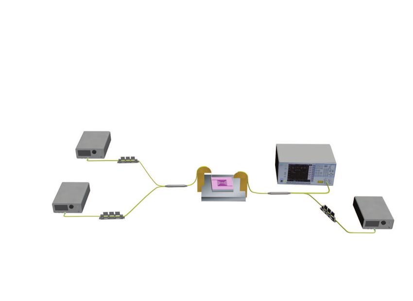
4

  [∗ ] These authors contributed equally to this Letter.                  and A. Polman, “Erbium-implanted high-q silica toroidal micro-
                                                                          cavity laser on a silicon chip,” Physical Review A 70, 033803
1 J.  D. Bradley and M. Pollnau, “Erbium-doped integrated waveg-          (2004).
   uide amplifiers and lasers,” Laser & Photonics Reviews 5, 368–      19 L. Agazzi, K. Worhoff,       and M. Pollnau, “Energy-transfer-
   403 (2011).                                                            upconversion models, their applicability and breakdown in the
 2 D. N. Nikogosyan, Nonlinear optical crystals: a complete survey
                                                                          presence of spectroscopically distinct ion classes: A case study in
   (Springer Science & Business Media, 2006).                             amorphous al2o3: Er3+,” The Journal of Physical Chemistry C
 3 A. Boes, B. Corcoran, L. Chang, J. Bowers, and A. Mitchell,
                                                                          117, 6759–6776 (2013).
   “Status and potential of lithium niobate on insulator (lnoi) for    20 J. Mu, M. Dijkstra, J. Korterik, H. Offerhaus,          and S. M.
   photonic integrated circuits,” Laser & Photonics Reviews 12,           Garcı́a-Blanco, “High-gain waveguide amplifiers in si3n4 technol-
   1700256 (2018).                                                        ogy via double-layer monolithic integration,” Photonics Research
 4 J. Lin, F. Bo, Y. Cheng, and J. Xu, “Advances in on-chip pho-
                                                                          8, 1634–1641 (2020).
   tonic devices based on lithium niobate on insulator,” Photonics     21 J. Rönn, J. Zhang, W. Zhang, Z. Tu, A. Matikainen, X. Leroux,
   Research 8, 1910–1936 (2020).                                          E. Durán-Valdeiglesias, N. Vulliet, F. Boeuf, C. Alonso-Ramos,
 5 M. Zhang, C. Wang, R. Cheng, S. A. Amirhassan, and L. Marko,
                                                                          et al., “Erbium-doped hybrid waveguide amplifiers with net op-
   “Monolithic ultrahigh-q lithium niobate microring resonator,”          tical gain on a fully industrial 300 mm silicon nitride photonic
   Optica 4, 1536– (2017).                                                platform,” Optics Express 28, 27919–27926 (2020).
 6 R. Luo, Y. He, H. Liang, M. Li, and Q. Lin, “Highly tunable effi-
                                                                       22 S. A. Vázquez-Córdova, M. Dijkstra, E. H. Bernhardi, F. Ay,
   cient second-harmonic generation in a lithium niobate nanopho-         K. Wörhoff, J. L. Herek, S. M. Garcı́a-Blanco, and M. Poll-
   tonic waveguide,” Optica 5, 1006–1011 (2018).                          nau, “Erbium-doped spiral amplifiers with 20 db of net gain on
 7 X. Ye, S. Liu, Y. Chen, Y. Zheng, and X. Chen, “Sum-frequency
                                                                          silicon,” Optics Express 22, 25993–26004 (2014).
   generation in lithium-niobate-on-insulator microdisk via modal      23 J. Rönn, W. Zhang, A. Autere, X. Leroux, L. Pakarinen,
   phase matching,” Optics Letters 45, 523–526 (2020).                    C. Alonso-Ramos, A. Säynätjoki, H. Lipsanen, L. Vivien, E. Cas-
 8 L. Ge, Y. Chen, H. Jiang, G. Li, B. Zhu, X. Chen, et al., “Broad-
                                                                          san, et al., “Ultra-high on-chip optical gain in erbium-based hy-
   band quasi-phase matching in a mgo:ppln thin film,” Photonics          brid slot waveguides,” Nature Communications 10, 1–9 (2019).
   Research 6, 954–958 (2018).                                         24 Y. Liu, X. Yan, J. Wu, B. Zhu, Y. Chen, and X. Chen, “On-
 9 J. Lin, Y. Xu, J. Ni, M. Wang, Z. Fang, L. Qiao, W. Fang,
                                                                          chip erbium-doped lithium niobate microcavity laser,” SCIENCE
   and Y. Cheng, “Phase-matched second-harmonic generation in             CHINA Physics, Mechanics & Astronomy 64, 1–5 (2021).
   an on-chip l i nbo 3 microresonator,” Physical Review Applied       25 Z. Wang, Z. Fang, Z. Liu, W. Chu, Y. Zhou, J. Zhang, R. Wu,
   6, 014002 (2016).                                                      M. Wang, T. Lu, and Y. Cheng, “On-chip tunable microdisk
10 J. Lin, N. Yao, Z. Hao, J. Zhang, W. Mao, M. Wang, W. Chu,
                                                                          laser fabricated on er3+-doped lithium niobate on insulator,”
   R. Wu, Z. Fang, L. Qiao, et al., “Broadband quasi-phase-matched        Optics Letters 46, 380–383 (2021).
   harmonic generation in an on-chip monocrystalline lithium nio-      26 D. Yin, Y. Zhou, Z. Liu, Z. Wang, H. Zhang, Z. Fang, W. Chu,
   bate microdisk resonator,” Physical Review Letters 122, 173903         R. Wu, J. Zhang, W. Chen, et al., “Electro-optically tunable
   (2019).                                                                microring laser monolithically integrated on lithium niobate on
11 M. Xu, M. He, H. Zhang, J. Jian, Y. Pan, X. Liu, L. Chen,
                                                                          insulator,” Optics Letters 46, 2127–2130 (2021).
   X. Meng, H. Chen, Z. Li, et al., “High-performance coherent         27 Q. Luo, C. Ya, R. Zhang, Z. Hao, D. Zheng, H. Liu, X. Yu,
   optical modulators based on thin-film lithium niobate platform,”       F. Gao, F. Bo, Y. Kong, et al., “On-chip erbium-doped lithium
   Nature communications 11, 1–7 (2020).                                  niobate microring lasers,” arXiv preprint arXiv:2103.09558
12 M. Li, J. Ling, Y. He, U. A. Javid, S. Xue, and Q. Lin, “Lithium
                                                                          (2021).
   niobate photonic-crystal electro-optic modulator,” Nature Com-      28 Q. Luo, Z. Z. Hao, C. Yang, R. Zhang, and J. J. Xu, “Microdisk
   munications 11, 1–8 (2020).                                            lasers on an erbium-doped lithium-niobite chip,” Science China:
13 C. Wang, M. Zhang, X. Chen, M. Bertrand, A. Shams-Ansari,
                                                                          Physics, Mechanics and Astronomy 64 (2021).
   S. Chandrasekhar, P. Winzer, and M. Lončar, “Integrated            29 Z. Chen, Q. Xu, K. Zhang, W.-H. Wong, D.-L. Zhang, E. Y.-B.
   lithium niobate electro-optic modulators operating at cmos-            Pun, and C. Wang, “Efficient erbium-doped thin-film lithium
   compatible voltages,” Nature 562, 101–104 (2018).                      niobate waveguide amplifiers,” Optics Letters 46, 1161–1164
14 B. Pan, J. Hu, Y. Huang, L. Song, J. Wang, P. Chen, L. Liu, and
                                                                          (2021).
   D. Dai, “The first demonstration of high-speed linbo3 thin-film     30 J. Zhou, Y. Liang, Z. Liu, W. Chu, H. Zhang, D. Yin, Z. Fang,
   optical modulators operating at the wavelength of 2 µm,” in Asia       R. Wu, J. Zhang, W. Chen, et al., “On-chip integrated waveguide
   Communications and Photonics Conference (Optical Society of            amplifiers on erbium-doped thin film lithium niobate on insula-
   America, 2020) pp. M4D–7.                                              tor,” arXiv preprint arXiv:2101.00783 (2021).
15 C. Wang, M. Zhang, M. Yu, R. Zhu, H. Hu, and M. Loncar,
                                                                       31 Q. Luo, C. Yang, Z. Hao, R. Zhang, D. Zheng, F. Bo, Y. Kong,
   “Monolithic lithium niobate photonic circuits for kerr frequency       G. Zhang, and J. Xu, “On-chip erbium-doped lithium niobate
   comb generation and modulation,” Nature Communications 10,             waveguide amplifiers,” arXiv preprint arXiv:2103.15786 (2021).
   1–6 (2019).                                                         32 D. L. Zhang, F. Han, B. Chen, P. R. Hua, D. Y. Yu,             and
16 Z. Fang, H. Luo, J. Lin, M. Wang, J. Zhang, R. Wu, J. Zhou,
                                                                          Y. B. Pun, “Optical-damage-resistant highly er -doped ti:er:linbo
   W. Chu, T. Lu, and Y. Cheng, “Efficient electro-optical tuning         strip waveguide,” Journal of Lightwave Technology 32, 135–140
   of an optical frequency microcomb on a monolithically integrated       (2013).
   high-q lithium niobate microdisk,” Optics Letters 44, 5953–5956     33 D. Brüske, S. Suntsov, C. Rüter, and D. Kip, “Efficient ridge
   (2019).                                                                waveguide amplifiers and lasers in er-doped lithium niobate by
17 Y. He, Q. F. Yang, J. Ling, R. Luo, and Q. Lin, “Self-starting
                                                                          optical grade dicing and three-side er and ti in-diffusion,” Optics
   bi-chromatic linbo3 soliton microcomb,” Optica 6, 1138 (2019).         Express 25, 29374 (2017).
18 B. Min, T. J. Kippenberg, L. Yang, K. J. Vahala, J. Kalkman,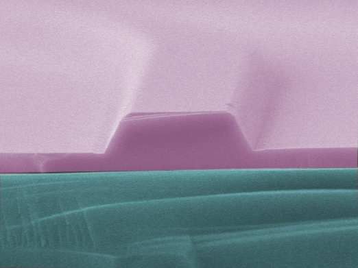
You can also read