ASIC Test Oriented Simulation Manual - Microchip Technology
←
→
Page content transcription
If your browser does not render page correctly, please read the page content below
ASIC Test Oriented Simulation Manual

Introduction
A challenge of testing application-specific ICs is creating test patterns by IC-design engineers who do not have deep
knowledge of the test-equipment and the related requirements and restrictions.
This manual bridges the gap by providing explanations, examples, and the necessary information to successfully set
up and perform simulations, which must be usable for testprogram-generation. It also explains the Microchip-internal
transformation-flow and the tools involved.

Terminology
The following terms are used frequently to identify specific test features and constraints:

 Terminology                   Description
 ATE                           Automatic Test Equipment (ATE). A tester is an ATE.
 DUT                           Device Under Test (DUT)
                               A hardware product verified on the tester. It can either be a die on a wafer or a
                               packaged part.

 Wafer Probe                   Testing operation for die on wafers.
                               It uses an additional ATE named Prober and a DUT interface named Probe Card.

 Final Test                    Testing operation for packaged parts after assembly.
                               It uses a DUT interface named Load Board.

 Test Cycle                    The interval of time (also called period) in which a test vector is presented to the DUT.
                               The beginning of a Test Cycle is the reference time for relative timings.

 Test Vector                   A Test Vector consists of one signal state line in a test pattern.
                               It contains:
                               A period that delimits the beginning and end of the test vector, also called Test Cycle.
                               Signal states. Each signal state is represented by a symbol, which reflects its level and
                               direction (input or output mode for bidirectional). See Waveform File Format for more
                               information about symbols.
                               Timing data. Each signal has its own timing data. Inputs are stimulated at predefined
                               times (driven by the hardware of the tester), and outputs are sampled at predefined
                               Strobe times.

 Test Pattern                  This is a set of test vectors, usually composed of one or two files: one for the signal
                               states and one for the timing information. They are the results from the conversion
                               of a simulation. The very first test vector starts at time 0, which is the absolute time
                               (reference) for the pattern.

© 2021 Microchip Technology Inc.                              Manual                                    DS50003170A-page 1
and its subsidiaries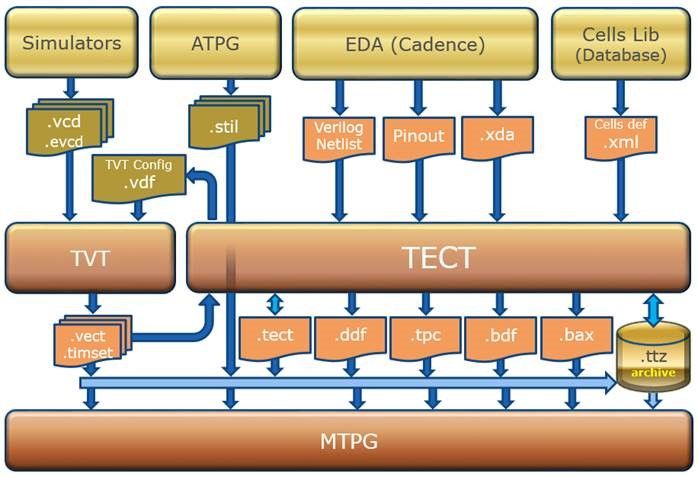
...........continued
 Terminology                   Description
 Tset                          Tset or Timing Set
                               It is the (named) identification of all timing data for a given test vector. Testers have a
                               hardware limitation for the maximum number of Tsets in general.

 Fset                          Fset or Format Set
                               It is the combination of formats of all signals (that is, input mode, output mode or
                               undriven mode) at a given test vector. The Fsets can change from one test vector to
                               the next one. However, testers have a hardware limitation for the maximum number of
                               Fsets. In order to avoid violating the maximum number of Fsets, it is recommended to
                               carefully check the direction of bidirectional ports in the simulations.

 TOS                           Test Oriented Simulation (TOS)
                               A specific simulation performed by the designer to build the corresponding test pattern,
                               which is intended to run on the ATE.

 NRZ                           Non-Return to Zero (NRZ)
                               Format of a signal which has only a single event transition (at a given time) in a test
                               vector.

 RTZ                           Return To Zero (RTZ)
                               Format of a signal, which may have two event transitions, the first to go to HIGH state,
                               and the second to return to LOW (Zero) state.

 RTO                           Return To One (RTO)
                               Format of a signal, which may have two event transitions, the first to go to LOW state,
                               and the second to return to HIGH (One) state.

Advice
Copyright 2021 by Microchip Nantes S.A., printed in France
All rights reserved. No part of this publication may be reproduced, stored in a retrieval system, or transmitted in any
form or by any means without prior written permission from Microchip Nantes S.A.
DISCLAIMER
The information in this document is subject to change without notice and should not be construed as a commitment of
Microchip Nantes S.A. The reader should, in all cases, consult Microchip Nantes to determine whether any changes
have been made.
NOTICE
This documentation for Microchip Nantes software proprietary product (programs, libraries) is subject to the
conditions of a Software License Agreement, and may be used only by licensees and their employees. Access
to Microchip Nantes documents by other persons is prohibited.
As provided in the Software License Agreement, no copies of the software and documentation may be made, in
whole or part, without express written permission of Microchip Nantes S.A. The license is attached to a "Design
Development", it starts at the "Project Order Entry" date and expires at the "Design Approval" date.
To prevent confusion because of multiple versions and to control unauthorized access and use, all copies of previous
versions of the documentation should be destroyed by the licensee of the product, upon receipt of the latest version.
MICROCHIP NANTES SOFTWARE SUPPORT
Contact the ASIC Field Application Engineer in your local Microchip Technical Center office.

© 2021 Microchip Technology Inc.                               Manual                                    DS50003170A-page 2
and its subsidiaries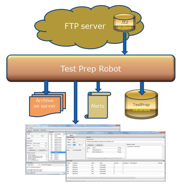
To ensure accurate and expedient assistance with your questions or problems, please use the hotline call electronic
form.
TRADEMARKS
GATEAID2, OPEN ASIC are trademarks of Microchip Nantes S.A.
CADENCE, MENTOR GRAPHICS, SUN, SYNOPSYS are registered trademarks.

© 2021 Microchip Technology Inc.                          Manual                                 DS50003170A-page 3
and its subsidiaries
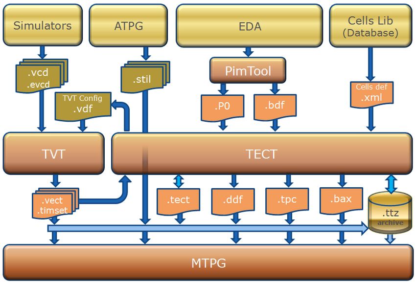
Table of Contents
Introduction.....................................................................................................................................................1
      1.         Terminology.................................................................................................................................. 1
      2.         Advice ..........................................................................................................................................2

1.    Product Testing....................................................................................................................................... 6
      1.1.       Design Cycle................................................................................................................................ 6
      1.2.       TOS Guidelines............................................................................................................................ 6
      1.3.       MICROCHIP Test Equipment ...................................................................................................... 7

2.    TOS Rules...............................................................................................................................................9
      2.1.       What is TECT?............................................................................................................................. 9
      2.2.       Design to Test Flow...................................................................................................................... 9
      2.3.       TECT Startup............................................................................................................................... 9
      2.4.       TECT Tabs................................................................................................................................. 10
      2.5.       TECT Flow..................................................................................................................................11
      2.6.       TECT Files (Bonded Packages).................................................................................................12
      2.7.       TECT Files (Flipchip Packages).................................................................................................13
      2.8.       Test Prep Flow............................................................................................................................13
      2.9.       Burn-in Board and Patterns Definition........................................................................................14

3.    Test Patterns......................................................................................................................................... 15
      3.1.       VCD Rules..................................................................................................................................15
      3.2.       Patterns Order............................................................................................................................16

4.    Tests Tab............................................................................................................................................... 17
      4.1.       DC Tests.....................................................................................................................................17
      4.2.       AC Tests – Dynamic Timing Measurements...............................................................................17
      4.3.       Idd Tests – StandBy, Dynamic, or Iddq Current Measurements.................................................18

5.    TECT Completion..................................................................................................................................20
      5.1.       Checks....................................................................................................................................... 20
      5.2.       Save........................................................................................................................................... 20
      5.3.       Archive....................................................................................................................................... 20

6.    TECT Rules...........................................................................................................................................21

7.    Appendix............................................................................................................................................... 24
      7.1.       Simultaneous Switching Outputs................................................................................................24
      7.2.       Vref Pins.....................................................................................................................................24
      7.3.       DFT and Coverage.....................................................................................................................24

8.    Conclusion............................................................................................................................................ 25

9.    Revision History.................................................................................................................................... 26

The Microchip Website.................................................................................................................................28

Product Change Notification Service............................................................................................................28

© 2021 Microchip Technology Inc.                                                         Manual                                                       DS50003170A-page 4
and its subsidiaries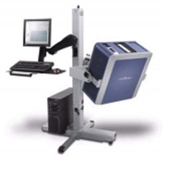
Customer Support........................................................................................................................................ 28

Microchip Devices Code Protection Feature................................................................................................ 28

Legal Notice................................................................................................................................................. 29

Trademarks.................................................................................................................................................. 29

Quality Management System....................................................................................................................... 30

Worldwide Sales and Service.......................................................................................................................31

© 2021 Microchip Technology Inc.                                                        Manual                                                     DS50003170A-page 5
and its subsidiaries
Product Testing

1.        Product Testing

1.1       Design Cycle
          The design cycle of a product consists of several operations, one of them being the functional simulation. Several
          kinds of functional simulations can be performed, some of them to check the product functionality (digital, analog
          or mixed signal) in its application environment, and some of them are dedicated to build a test program for chip
          verification after fabrication (TOS).
          TOS consist of several parts—Scan test, at-speed test, functional test, BIST, and so on. Each of them is either
          outputs from a golden simulator (such as VHDL or Verilog™) or from an automatic test pattern generator (ATPG)
          such as FastScan™ or TetraMax™.

1.1.1     TVT Overview
          The waveforms are generated in .vcd files or .stil files. The .vcd file format must be translated with Test
          Vector Translator (TVT) (part of Microchip Design Kit) into a proprietary Microchip format as a set of two files—VECT
          and TIMSET. Besides, the .stil format generated by most ATPG commercial tools can be directly transferred to
                                                   ®
          Microchip if it is restricted to the IEEE 1450.99 specification.

1.1.1.1   Sub-Nanosecond Times in TVT
          TVT and VECT-TIMSET files can support times less than a nanosecond. The minimal time unit in TVT is 1 ps. All
          times expressed with a fraction smaller than 1 ps are rounded.
          Using the minimal test resolution of 10 ps for simulations is a good compromise between simulation-time, precision,
          and file size.
          For the test-oriented simulations, this might cause differences between the minimum and maximum-simulations. It is
          recommended to first simulate with a precision of 1 ps to check, if the mismatch disappears before investigating in
          other directions.

1.1.2     TECT Overview
          Test Entities Configuration Tools (TECT) is used (also part of Microchip Design Kit) to manage and transfer product
          files to Microchip Technical Center. It includes a series of verifiers to check simulation results and other special DC
          and AC test requirements. You will find some TECT information in this document, and more details in the TECT User
          Manual.
          After file transfer to Microchip, they are combined into a test program that runs onto a tester. The tester provides
          a method to certify that the hardware product is functional after fabrication in the given environment (temperature,
          voltage, radiation, life test, and so on). These tests are run first at wafer level (wafer probe), then after assembly at
          device level (final test).

1.2       TOS Guidelines
          To stimulate a device off its final application board, a series of logical vectors must be applied to the device inputs.
          These are called test vectors that are used to stimulate the design inputs and check the outputs against the expected
          values. In other words, on a tester the test vectors replace the HDL test bench (used by designers) to verify the
          design functionality.
          Microchip sets some rules and formats for customers to generate test vectors. A standardized format helps
          customers and Microchip to:
            •   Improve simulation by reducing errors
            •   Simplify design verification on ATE
            •   Reduce project cycle times
            •   Reduce debugging costs
          This document provides guidelines for test vector sets. These are recommended for functional verification of ASIC
          designs made with Microchip and cover several aspects of design verification including:

          © 2021 Microchip Technology Inc.                              Manual                                    DS50003170A-page 6
          and its subsidiaries
Product Testing
• Waveform file format
• Tester constraints
• Mandatory tools to use—TVT and TECT
• Simultaneously switching outputs (in Appendix)
1.2.1 Waveform File Format
The vector file (VECT) is a text file that contains binary values of all signals of the device. Each line of the file forms a
test vector, which indicates the state of all ports at a given test cycle.
Individual signal entries in each line must use the following characters:
• Inputs—0, 1, D or U
• Outputs—L, H, Z or X (tested states)
• Bidirectional—either 0, 1, D or U (input mode) or L, H, Z or X (output mode)
1.2.2 Tester Constraints
The vector files are applied to the device using the tester (ATE) as described in Microchip Test Equipment. The tester
limitations along with general hardware considerations imply constraints, which must be considered during the test
vector generation.
The tester activities such as applying input signals and reading back the outputs of the design are synchronous to a
reference clock, which is extracted from the vector file. Therefore, synchronous vector files are always required.
As the vector files must always be synchronous, care must be taken in generating vectors for signals, which are
asynchronous in the application. The asynchronous inputs must be applied in the test vectors synchronously to the
tester cycle and outputs will be sampled synchronously to the tester cycle.
As with asynchronous inputs, you must check if multiple clock inputs to the design are asynchronous with respect to
each other. Due to the synchronous nature of the vector files, the asynchronous clocks may be affected by missing
edges with respect to the reference clock. As a result, clocks must be synchronized to avoid errors.
1.2.3 Analog IPs
The test of the analog IPs must be considered during the code-development phase. For more information on
integration and test strategy, see the IP’s datasheet. Support and additional information can be provided at the
Microchip local design center.
1.3 MICROCHIP Test Equipment
For testing the high complexity circuits such as those using MICROCHIP ASIC families, the following tester will be
used: Cohu D10 (100 MHz, up to 200 Mbits/sec, 672 digital pins, accurate DC measurements with VIS16 option).
A tester specification datasheet can be provided on request.
© 2021 Microchip Technology Inc. Manual DS50003170A-page 7
and its subsidiariesProduct Testing Figure 1-1. Cohu D10 Test Equipment © 2021 Microchip Technology Inc. Manual DS50003170A-page 8 and its subsidiaries
TOS Rules
2. TOS Rules
Most testers have hardware and software restrictions and limitations that designers must take into consideration.
These restrictions and rules must be checked as early as possible in the TOS design cycle with Microchip’s TVT and
TECT tools.
2.1 What is TECT?
Since 2014, Test Entities Configuration Tools (TECT) is a utility tool between design and test environments.
TECT collects design data files such as simulation results, and several other product description files, to build a
package to be transferred to Microchip Technical Center then to Test Engineering to generate test programs.
TECT includes built-in interactive verifiers that check data consistencies and various causes of error, and it creates
error reports.
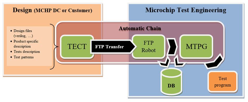
2.2 Design to Test Flow
The following figure shows where TECT is in the test program generation flow:
TECT is designed to use in an interactive way. It is delivered as part of Microchip Design Kits (DK). See the TECT
User Manual for more information about installation and usage.
Usually, at the beginning of a project for a new product, the Microchip Technical Center receives a pin list from the
customer. The Microchip Technical Center analyses the pin list and starts working with TECT. TECT supports several
processes (from 0.15 µm to 65 nm) and the technology choice is the starting point.
Microchip’s TECT archive, by Microchip’s DC, is transferred back to the customer to finish the remaining tasks.
2.3 TECT Startup
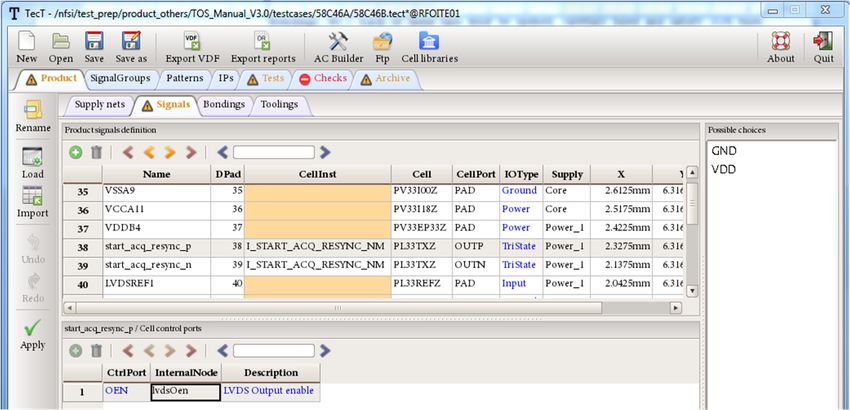
The graphical user interface of TECT consists of a series of primary tabs (Product, SignalGroups, Patterns, and so
on) and a series of secondary tabs (Supply nets, Signals, Bondings, and so on). Each of these tabs must be opened
and filled to satisfy TOS rules, before navigating to the next tab.
© 2021 Microchip Technology Inc. Manual DS50003170A-page 9
and its subsidiariesTOS Rules
You can see various tabs in the following image:
The different tabs show an attached symbol:
• Indicates, if there is a missing information (for example, CellInst is missing).
• Indicates, if an error was detected that must be fixed (for example, an AC Check for which the signal
transitions are not present in the corresponding test pattern).
2.4 TECT Tabs
The TECT tabs are named as:
• Product: Definition of the product and the following sub-tabs:
– Supply nets: Set voltages (Typ, Min, and Max) for all supply ports (Note 1).
– Signals: External I/Os and all associated information, including internal control ports (Note 1).
– Bondings: Package pin lists (Note 2).
– Toolings: Tester hardware interfaces. Wafer Probe Cards, Device Load Boards, and Burn-In Boards are
Microchip’s responsibility (See TECT Manual).
• SignalGroups (optional): To help designer to group signals together.
• Patterns: Definition of the TOS patterns to be used in the test program.
– Defines the format and the use of each pattern.
• IPs: Definition of additional IP information such as LVDS pairs and reference voltages (Note 3).
• Tests: Access to three sub-tasks: DC Tests, AC Tests, and Idd Tests.
– DC Tests: Allow selection of dedicated patterns for DC tests.
– AC Tests: Manage all AC tests to be performed.
– Idd Tests: Manage Idd StandBy, (Dyn) Operating Idd, and Iddq measurements.
• Checks: Click the Check All button to perform all possible checks.
• Archive: Builds a TECT database for transfer to Microchip Technical Center (See Test Prep Flow).
See the TECT User Manual for more information.
Note 1: This information can be uploaded automatically from the .P0 file (output from PIMTOOL). When the .P0 file
is not filled correctly (for example, internal control ports are often missing), you can import the Verilog description (.v
file), which contains the top module of the product.
© 2021 Microchip Technology Inc. Manual DS50003170A-page 10
and its subsidiariesTOS Rules
Note 2: The bonding information (connections between die signals to package pins) can be entered automatically
from the .bdf file (output from PIMTOOL).
Note 3: For all LVDS I/O ports, it is mandatory to identify the external voltage reference pins, except if the given
reference voltage is internally generated.
For each pair during simulation, the N and P pins must be stimulated, one at the inverse state than the other. Ensure
that the external reference voltage pins must be present in the netlist and driven to logical 1.
2.5 TECT Flow
The TECT flow consists of the following steps:
• An initial .vdf file for TVT is generated by TECT.
• TVT generates patterns in VECT-TIMSET file format, from designer’s simulation provided in .vcd or .evcd file
formats.
®
• The .stil files are only verified by TECT for their IEEE 1450.99 compliance, then transferred to the TTZ
database.
• The TTZ database is a zipped tarball of all necessary files to transfer to the Microchip Technical Center. This
database is encrypted by default for transfer security. However, the encryption may be disabled.
• The Modular Test Program Generator (MTPG) requires DDF file, BDF file, and patterns in VECT-TIMSET and/or
STIL formats. The TPC file gives an additional information about the test program to be generated. All these files
are packaged and compressed in the TTZ database file.
• After place and route operation, the pad locations (X-Y coordinates of the wire bonding areas) are known
and written in the .ddf file. They are required in TECT, prior to transfer the TTZ database to your Microchip
Technical Center. They are used to build the Probe Card documents. Instead of the .ddf file, you may also
receive a .coord file that provides the required X-Y coordinates of the wire bonding areas.
© 2021 Microchip Technology Inc. Manual DS50003170A-page 11
and its subsidiariesTOS Rules
2.6 TECT Files (Bonded Packages)
Note: This flow with PimTool applies for standard bonded packages (For Flipchip-Packages, see here below).
© 2021 Microchip Technology Inc. Manual DS50003170A-page 12
and its subsidiariesTOS Rules
2.7 TECT Files (Flipchip Packages)
2.8 Test Prep Flow
At the end of the TECT flow, the TTZ archive database must be transferred through FTP to the Microchip Technical
Center.
The following figure shows what happens with the TTZ archive after transfer:
• The files in the TTZ archive are backed up on a secured Microchip server and recorded in Microchip’s Test Prep
database.
• A Microchip Graphical User Interface shows the status of files.
• The Microchip MTPG is used to build the appropriate test program for the target ATE.
• A Microchip Test Engineer checks the test program with actual parts on the target tester.
© 2021 Microchip Technology Inc. Manual DS50003170A-page 13
and its subsidiariesTOS Rules
2.9 Burn-in Board and Patterns Definition
Microchip provides multiple kinds of ovens with different testing capabilities (burn-in with test, individual temperature
control).
For now, TECT only provides an interface for the Criteria and MCC ovens, for all other kinds of hardware, burn-in
board, and dedicated patterns must be done outside TECT control.
See the Microchip DSGE 003 specification, Burn-in Board Definition for more information.
© 2021 Microchip Technology Inc. Manual DS50003170A-page 14
and its subsidiariesTest Patterns
3. Test Patterns
Each test pattern consists of a set of test vectors. A test vector is a combination of inputs/outputs within a test cycle
named period. In this test cycle, the inputs are FORCED (driven) by the tester, while the outputs are STROBED
(sampled) and compared to the expected states.
The test vectors must be checked by comparing the simulations in worst case against the best case, and must take
into account the delay back annotation (.sdf file) after chip place and route.
All patterns used for DC tests must use static vectors. There must be enough time to ensure stable outputs after
changing the inputs.
The outputs are usually sampled (at Strobe time) at the end of the test vector (90% of the period).
The following two file formats are supported:
• STIL format (Only IEEE 1450.99 version) for scan test vectors (Stuck-At fault model or Transition Delay fault
model), generated by an ATPG after scan insertion. The STIL file format also supports the specific keyword
IddqTestPoint, generated by the appropriate IDDQ tool, to generate the corresponding Iddq measurements in
the test program.
• VECT-TIMSET format (VCD or EVCD file format translated by TVT into two files .vect and .timset) for
functional test vectors or BIST. This is a Microchip proprietary file format, which consists of two files. Both VECT
and TIMSET files must be identified in TECT to make one test pattern.
Useful TECT buttons for the Patterns tab:
• Scan Dir: Scans for all patterns (simulation results) present in a given directory.
• Browse: Opens directories to find and select pattern files.
• Preserve STIL scan chains: (only for STIL patterns), can be used if the target tester supports the scan chain
feature.
The customer is responsible for the global product test coverage. When the test coverage of a pattern is known, you
must provide it in the Coverage field of the pattern.
Some other possibilities are supported, see the TECT User Manual.
3.1 VCD Rules
Most testers have limitations in terms of Tsets and Fsets. The product designer must follow the recommendations
(Best practices) to avoid the excessive use of Tsets and Fsets:
Best Practice 1:
Input signals: Ensure that all input events (transitions driven by the ATE) change state at the same relative time with
respect to the beginning of the test cycles, which must be periodic over all your simulation.
Note: TDF (for Transition Delay Fault detection) patterns (usually in .stil format, not .vcd) do not follow this rule.
Best Practice 2:
Clock signals: Avoid setting active clock edges at the very beginning (time 0) or very end of test cycles. The
chronologic scheme must always be:
1. Initializing the data signals first (ideally at the very beginning of the cycle).
2. Then the active clock-edge. However, try to keep it in the first half of the cycle to limit the best case/worst case
differences due to timing delay increases.
© 2021 Microchip Technology Inc. Manual DS50003170A-page 15
and its subsidiariesTest Patterns
Best Practice 3:
Bidir signals: Always make a bidir pin tristate (drive Z) mode (at the same time as inputs) when switching direction
from input to output. For instance, drive a Z state at 5.0 ns, if the other input pins are changing at 5.0 ns. There is not
such restriction on the strobe time.
Best Practice 4:
Bidir signals: Always make a bidirectional bus to switch direction all together (all bits of the bus at the same time)
from input to output, or vice-versa. This is to reduce the number of format sets reserved by the tester.
Best Practice 5:
Never simulate with pull-up/pull-down models. On-chip pulls are too weak and test board is not equipped with any
resistor. This leads to errors during test.
TVT checks the rules so that testing your product is possible on every available tester.
Input timings and output strobes are controlled by customer simulation testbench. The customer generates
waveforms that are suitable to meet the required functionality and fault coverage.
3.2 Patterns Order
Even if TECT tracks the patterns order, ensure that the test program does not execute them in a totally different order
depending on the test flow. For example, patterns used by AC tests are executed multiple times at different moments
of the test flow.
To avoid side effects due to pattern order execution, each pattern must begin by a reset sequence, which guarantees
that DUT is in a stable state before the test execution.
There is no constraint on pattern length (vector count). But for any reason, a pattern has to be split into multiple
sub-patterns, the reset sequence is mandatory only on the first part.
Execution order of different patterns must be specified in TECT in the comment field attached to the pattern. As a
result, DC and AC tests cannot be done on sub-patterns due to the lack of the reset sequence.
© 2021 Microchip Technology Inc. Manual DS50003170A-page 16
and its subsidiariesTests Tab
4. Tests Tab
TECT contains three different categories under the Tests tab: DC Tests, AC Tests, and Idd.
4.1 DC Tests
The aim of DC tests is to perform all possible static DC measurements to confirm that the DC specifications are
addressed. The goal is 100% coverage in all possible configurations. A recommended practice is to build only one
dedicated DC Tests functional simulation to perform all DC tests.
SCAN or TDF simulations in STIL format, are not suitable for DC test measurements. Simulations requiring 4x mode
usage are also not suitable for DC test.
DC tests must be performed on all external pins of the product, in all possible configurations. DC tests of SCAN in
and SCAN out pins can be performed by a serial shift test of the sequence 00110011 (usually provided as the first
scan chain sanity check). This validation must be provided as part of a DC tests dedicated functional simulation.
DC tests pattern(s) requires a specific simulation built where all internal control ports must be traced in the .vcd file.
The TVT setup must be setup (using a specific flag) accordingly to translate the state of these internal nodes into the
output VECT-TIMSET files. It is also recommended to unset this flag for the remaining patterns (those that are not
used for DC tests).
In some cases, the configuration requirement may be difficult to satisfy, but it is the designer’s responsibility to
achieve the best DC Tests coverage (ideally 100%). The report file dctReport.txt is provided to help finding the
missing states or conditions for each signal. A detailed explanation is required for all signals that do not fulfill this DC
test requirement.
The difficulty occurs especially with configurable I/O cells (see the next chapter 4.1.2), which have multiple control
ports. To meet the 100% coverage requirement for DC test, all possible combinations of the control ports must be
exercised during the simulation. The waveforms of these internal signals must be translated by TVT into Microchip
VECT format, so the Test Program Generator can find the required conditions for DC tests.
4.1.1 Bidirectional Ports
The drive direction of the bidirectional ports is defined by their bidirectional I/O buffer control signal, usually an
internal signal. As mentioned, the tester is unable to both drive and sample within a given cycle. Therefore, control
signals must be monitored during the test vector generation whether they are internal signals or external inputs to the
design. When none of the external ports can indicate the status of the bidirectional I/O control signals at each time,
the control signals must be brought out to the testbench level through creating virtual output ports in the top-level of
the design and connect the control signals to the ports. The control signal can then be read and monitored in the
testbench level for test vector generation.
4.1.2 Configurable Cells
The configurable I/O cells (also called programmable buffers) include amongst other:
• A switchable pull-up resistor
• A switchable pull-down resistor
• Selectable drive strengths for output
in addition to a direction control for bidirectional port and a tri-state control, and possibly more. Consequently, the
number of control ports may be quite high. All configuration modes must be exercised for each specific buffer.
All internal control signals must be present in the simulation results (monitored in Verilog VCD files), except those that
are permanently tied to logical level high or low. In addition, all these internal ports must be switched to their different
states in the DC test simulation, because DC tests require these setups to perform the corresponding measurements.
4.2 AC Tests – Dynamic Timing Measurements
It is possible to generate a test program with automatic inclusion of AC test measurements, such as propagation
delay time, setup time, and hold time. These measurements are detailed in the P file format specification. Read this
specification to see the requirements for these measurements.
© 2021 Microchip Technology Inc. Manual DS50003170A-page 17
and its subsidiariesTests Tab
TECT provides a simple method to define these AC tests with all the required data. See the TECT User Manual for
more information about the fields of the user interface.
4.2.1 ATE Limitations
As not all testers are equipped with a specific timing measurement unit, the generic test method is to get an indirect
measure by moving edges placement (search method). This method may consume a lot of tester timing resources.
As these resources are limited, the number of AC tests must be reduced to a minimal set. A good practice is to limit
the number of timing measurements to less than 10 or 15.
4.2.2 AC Tests Range
AC tests can be performed on three different modes:
• Single: AC test is performed only once at a given time.
• Range: AC test is performed several times between the start and the stop time. The worst case is reported.
• All: AC test is performed along the whole selected pattern (from time 0 to the end of pattern).
Note: The Event Position parameter must be specified in absolute time values (relative to time 0 of the simulation)
for the Test Range Single, but specified in relative values (relative to the beginning of current test cycle) for other Test
Range modes.
If the AC tests have already been defined in the .P0 file, the button Import P0 must be used to load them into TECT.
Also, you can create the AC tests by clicking the Add button
Depending on the type of AC test, there are three possible signals:
• R (Reference signal—always an input), always used as base for measurements
• D (Data signal—always an input)
• O (Output signal—strobe time)
A propagation delay measurements (TP) uses only R and O. The tester is moving O strobe (search feature) towards
R as long as O satisfies the expected state. The measured timing is recorded when O fails.
A setup time (TS) or a hold time (TH) measurement is performed by moving the transition event of D (driven input)
towards R as long as O satisfies the expected state. The measured setup or hold time is recorded when O fails.
The differential propagation delay allows to compute the difference between two AC tests results. Obviously, the two
corresponding AC tests must be defined first.
Click Check all to verify that the AC Tests are correctly defined and check for the appropriate signal transitions in the
given pattern.
If a range (measurement between specified start and stop time) is selected, ensure that for the same set of signals,
there cannot be overlaps of two different AC tests ranges in the same pattern.
4.3 Idd Tests – StandBy, Dynamic, or Iddq Current Measurements
The Idd Tests can be:
• StandBy Idd for standby mode current measurements.
• Dynamic Idd operating current measurement in application mode (≥ 100 samples).
• Iddq measurement mode for predefined quiescent current measurement points.
TECT provides the appropriate setup for all Idd test types under the Idd tab. Idd measurements can be setup in
TECT for automatic test generation with the MTPG.
4.3.1 StandBy Current
StandBy Idd must be measured at a given time, at which the product is put in quiescent (or sleep) mode. It requires
to indicate the pattern to use and the appropriate time for this measurement.
If the StandBy current test is to be performed, a simulation must exist that includes a vector suitable for this test.
Such a simulation can be any simulation intended for a functional test. Ensure that the goal is to measure as less
current as possible. So, the presence of a pull-up or a pull-down resistor must be considered in the measurement
© 2021 Microchip Technology Inc. Manual DS50003170A-page 18
and its subsidiariesTests Tab
current estimation. It is recommended that ports with pull-down resistor are set low and ports with pull-up resistor are
set high on the chosen test vector. In addition, all static current sources must be disabled.
4.3.2 Dynamic Current
The operating Idd current measurement must be performed by specifying a functional pattern (typical product usage
in an application) and a time interval (from time – to time) during which the tester samples a series of measurements.
To obtain a good accuracy, the tester tries to perform at least 100 measurements in the given time interval. TECT
displays an error, if this requirement is not met.
4.3.3 Iddq Current
The Iddq measurements can automatically be generated if a .stil file is provided with the appropriate statements
in it. The required statement is IddqTestPoint, and there must be at least one of them in the STIL file. In addition, you
must specify the STIL pattern for Iddq usage in TECT in the Patterns tab, by selecting IDDQ.
Note: This feature communicates to the test program generator (MTPG) to include Iddq measurements, but there
is no corresponding consequences like binning. As a result, only values of the current measurement is reported. If
necessary, the limits and consequences must be added manually in the program later on.
If several Idd measurements must be done, it is required to setup as many Idd Tests as necessary. Each Idd Test has
a unique user configurable name.
© 2021 Microchip Technology Inc. Manual DS50003170A-page 19
and its subsidiariesTECT Completion
5. TECT Completion
5.1 Checks
TECT provides a powerful built-in verifier that checks many possible issues. The various checks that are performed
are given on the following pages in the section TECT Rules.
5.1.1 Complete Check
It is mandatory to perform a complete check by selecting the Check All button in this tab. After verification, save the
error log file by clicking the Report button.
The online checker looks for errors interactively. A red minus sign is shown on the tab button until all errors are fixed.
It is mandatory to fill in all the highlighted empty fields. Click on the light red area, then update the field by selecting
an item in the list presented on the right pane, or by typing the name of the internal signal.
5.2 Save
The Save or Save As buttons are used to save the changes made during the TECT session. It generates files with
the .tect and .tpc extensions, which can be read to retrieve the saved TECT session.
5.3 Archive
The Archive tab can be used to build a database file to be transferred. A zip compression option is used to reduce
the size of the archive file.
5.3.1 Pack
The Pack command on the left pane is used to build a package of the required files to transfer to the Microchip
Technical Center. This command is available only when all reported errors have been fixed. The revision number of
the package is automatically incremented at each time it is called.
• A window is presented in which it is required to select the appropriate patterns to add to the package (for
transfer).
• Optionally, a Comment field is provided to additional details of the package.
• The database is a compressed tarball with the .ttz extension. This file must be sent to Microchip Technical
Center.
TECT provides a built-in FTP client, which may be used to send the TTZ file. For security purposes, this FTP client
can optionally encrypt the file during transfer.
© 2021 Microchip Technology Inc. Manual DS50003170A-page 20
and its subsidiariesTECT Rules
6. TECT Rules
This list is non-exhaustive and can be updated as required. It is a list of rules that derive both from tester constraints
and limitations and from Microchip’s recommendations.
Product Description:
• Supply nets, Signals, and Bonding tabs must be free of errors (existence, consistency).
• X and Y coordinates may be omitted at first (Warning), but it is turned into an error at the final verification stage.
Signal Groups:
• No constraints for Signal Groups.
Test Patterns:
• VECT-TIMSET file format is allowed (Verilog simulations processed by TVT).
• STIL file format is allowed, when the IEEE 1450.99 standards are followed.
• All signals must be declared in patterns, including LVDS voltage reference.
• For a Cohu D10 tester, the minimum test cycle period is 10 ns. The test cycle period may violate these values,
then TECT is able to check if the special 4x Mode may be used. Indeed, this 4x Mode has a number of
additional constraints (indicated below) as it consists of building one test vector with two existing test vectors.
4x Mode Algorithm:
• This mode is available for VECT-TIMSET patterns (from TVT) only, as it is completely dependent on TVT
generated waveforms.
• The pattern period is multiplied by 2.
• The vectors are grouped by 2, therefore, it increases the number of transition edges in the waveforms of the
resulting vector (up to four transitions instead of two in the same test vector). For outputs, this may lead to
strobe twice in the same test vector.
Additional constraints related to this 4x mode:
• The number of vectors in each TIMSET must be an even number. If necessary, an extra vector must be added
to match this requirement.
• A limited number of waveform combinations is supported:
– NRZ: 0/0, 1/1, 1/0, 0/1
– RTZ: 0/0, U/0, 0/U, U/U
– RTO: 1/1, D/1, 1/D, D/D
– Strobe: L/L, H/H, H/L, L/H, X/X, X/L, L/X, X/H, H/X
Bidirectional signals support the following additional combinations:
X/0, 0/X, X/1, 1/X, X/U, U/X, X/D, D/X
Any other combination is not allowed.
• The bidirectional switching is only allowed on odd vectors, except if there is an X in the switch sequence (0/L
disallowed, 0/X/L allowed)
LVDS checks:
• Input and output pairs must be identified
• Voltage Reference (VREF) inputs must be identified
• DC coverage on output pairs must reach 100%. These tests include VOL_p/VOH_p and VOH_n/VOL_n on each
output pair. If 100% is not accomplished, a good reason with arguments must be provided.
DC Tests:
• DC Tests cannot be performed on STIL patterns.
• The patterns selected for DC tests must be made of static vectors.
• A single dedicated pattern for DC tests is recommended.
• If DC Tests coverage does not reach 100%, a good reason with arguments must be provided.
© 2021 Microchip Technology Inc. Manual DS50003170A-page 21
and its subsidiariesTECT Rules
AC Tests:
In AC Tests measurements, the tester loops over a given pattern and performs a series of measurements on the
same test cycle as long as it is necessary to find the worst case delay.
It is recommended using the AC builder button for creating AC tests. This ensures that all rules and constraints are
met. It analyses your simulations and checks for the required conditions for the given AC Test to be performed, alerts,
if the AC test can be performed or not, and fills the appropriate information.
In the following rules, the used terminology is listed:
• TG – Timing Generator: A tester hardware element, which accurately controls event transitions of input signals
(stimuli) and output strobe time (sampling).
• R – Reference: The reference event for the measurement. It must be an input signal.
• D – Data: is an input data, always an input signal.
• O – Output: An output data, a strobe to an output signal.
• R, D and O: A single or a group of signals (usually a bus). In this case, all signals of the same group must share
the same TG.
• Range or Test Range: Time interval in which the measurement will be done. By default, the measurement is
performed in a single test cycle (Single mode).
• TP or Propagation Delay: Indicates the type of measurement.
• TS or Setup Time: Indicates a Setup Time Measurement.
• TH or Hold Time: Indicates a Hold Time Measurement.
Rules for AC Tests:
• AC tests can only be performed on VECT - TIMSET patterns, not on STIL patterns.
• Rules (per test):
– For each signal (R, D, or O), the defined events must exist (the transition edge direction and the exact
timing information).
– For propagation delay measurement, the O signal must only depend on the R signal within the whole
Range.
– For hold and setup time measurements, the O signal must only depend on D signal within the whole
Range.
– If the Test range button is set to Single:
• Do not select Group for the R signal as all signals must share the same TG.
• Do not select Any edge type for the R signal as the edge type of a single signal on a single vector is
known (to be specified).
• Do not select Group for the D signal as all signals must share the same TG.
• Do not select Any edge type for the D signal as the edge type of a single signal on a single vector is
known (to be specified).
• If the O signal is a group signal, all signal states of the given group must switch in the test cycle. If
some signals do not switch, consider removing them from the group.
• If the O signal is a group signal and all signals have the same edge type, do not use Any as edge
type, but indicate the actual edge type.
• R/O events for TP must occur within the same test cycle
• R/D events for TS or TH must occur within the same cycle.
– If the Test range button is set to Range or All,
• The relative edge position (within the cycle) must remain the same within the whole range.
• Rules and constraints when multiple tests are declared:
– Two tests cannot be done on the same vector, if the same data or output signals are involved.
Dynamic Idd Tests:
• Dynamic Idd Tests cannot be done on STIL patterns.
• Time range for dynamic Idd tests must be wide enough to allow at least 100 samples.
• The tester minimal sampling rate is 4 µs (on D10) or 20 µs (on Sapphire).
© 2021 Microchip Technology Inc. Manual DS50003170A-page 22
and its subsidiariesTECT Rules Additional checks: • Number of available I/Os and powers on tester must match the product definition. • Number of scan chains must not exceed tester capability. • Pattern Memory consumption must not exceed tester capability. © 2021 Microchip Technology Inc. Manual DS50003170A-page 23 and its subsidiaries
Appendix

7.    Appendix

7.1   Simultaneous Switching Outputs
      Noise voltages in test equipment can sometimes be increased by many simultaneously switching outputs (SSO). To
      avoid triggering unintended device state changes, the number of SSOs in vector files must be minimized. Customers
      can reduce the number of SSOs during the test by avoiding unnecessary output switching. This can be done by
      controlling the enable signals to disable the unnecessary sections of the design.
      Note: The test vectors are usually generated to stimulate specific nodes or specific areas of the design.

7.2   Vref Pins
      Vref external pins must be present in the netlist, so that TVT uses them to generate the vectors and they are checked
      against opens, shorts, and ESD.
      It is recommended to maintain a logic 1 on these pins during simulation. The appropriate level is manually set by the
      test engineer. For MH1 library, the Vref pin must be declared as Tristate-Output (O/Z), and an X state must be applied
      during simulation. For other libraries, it must be declared as Input (I) and a level 1 must be applied during simulation.

7.3   DFT and Coverage
      The customer must demonstrate a design style and a design-for-test (DFT) methodology that, along with CAD for test
      tools, can provide 99% or greater fault coverage on a design of reasonable complexity. To achieve this, all available
      techniques can be used (Functional tests, At-Speed tests, ATPG = DFT scan, TDF = Transition Delay Fault tests, and
      so on).
      Objectives are to reach at least a test coverage of 80% for Transition Delay Fault (TDF) and 98% for stuck-at SCAN.
      As these values maybe unreachable due to design complexity or ATE limitations, these objectives may be lowered
      during the Design Review (DR).
      DFT tests and full scan ATPG tests implementation may induce physical phenomena such as voltage drop and
      high power consumption, and it may lead to discrepancies in test results. To address this possible problem, it is
      recommended to apply the appropriate specific techniques to minimize the simultaneous internal switching during
      scan tests.

      © 2021 Microchip Technology Inc.                            Manual                                  DS50003170A-page 24
      and its subsidiaries
Conclusion
8. Conclusion
The test strategy of the future circuits must be defined very early during the design phase. It is recommended to
contact the Technical Center to introduce the test constraints in the design, as soon as possible.
© 2021 Microchip Technology Inc. Manual DS50003170A-page 25
and its subsidiariesRevision History
9. Revision History
Revision Date Description
A 06/2021 The following sections are updated:
• Replaced Atmel references by Microchip.
• Remove reference to Sapphire tester.
• Added reference to MCC oven.
• Corrected some typos.
4.4 03/2017 Corrected an erroneous note about how to drive Lvds inputs in
simulations and some typos.
4.3 01/2017 The following sections were updated:
• Add patterns order and reset recommendations.
• Restrict 4X simulations usage for DC tests.
4.2 01/2016 The following sections were updated:
• Precision on 4X mode.
• Add references on external specifications (Burn-In)
4.1 01/2016 Precision on scan test coverage.
4.0.0 06/2015 The following sections were updated:
• Revision of the ASIC Test Manual
• Apply now to all Atmel Aerospace libraries
• Added new TECT features (Burn-In, Iddq)
3.0.0 01/2015 The following sections were updated:
• Introduce TECT as mandatory tool
• Table of contents has strongly changed
2.9.1 01/2014 Precision on test coverage responsibilities
2.9 02/2012 Tester support, Dynamic tests updates and limitations
2.8 04/2011 ADBI not authorized
2.7 04/2011 Changed ref. to ATD-DE-GR-R0324.
2.6 04/2011 Added AC Test Description
2.5 03/2011 Recommendation added for customer responsibilities.
2.4 11/2010 Test Guide is now separated from the design guide. It is updated for
TVT support, TPG and tester limitations
2.3 02/2010 Add SET mitigation in chapter 4 Design Rules
2.2 04/2008 LVDS buffer enable
2.1 03/2008 The following sections were updated:
• ATPG sim
• Remove 1% failing patterns
2.0 07/2007 Remove 1.8v Buffers and Add 2.5v Buffers
1.2 06/2006 SRAM/DPRAM/TPRegister read write cycles
© 2021 Microchip Technology Inc. Manual DS50003170A-page 26
and its subsidiariesRevision History
...........continued
Revision Date Description
1.1 04/2006 The following sections were updated:
• ESD protection considerations
• Double pad ring considerations
• Spare cells percentage StarRCXT
• Replaces HypeExtract & Fire&Ice ADBI paragraph removed
1.0 03/2005 The following sections were updated:
• Updated the timing specification
• Updated the genesys input desc.
0.3 Pre-production 12/2004 The following sections are updated:
• Design Management
• Power Rules
• TOS Rules
0.2 Beta 05/2004 Hardware considerations
0.1 Beta 03/2004 Initial Version
© 2021 Microchip Technology Inc. Manual DS50003170A-page 27
and its subsidiariesThe Microchip Website
Microchip provides online support via our website at www.microchip.com/. This website is used to make files and
information easily available to customers. Some of the content available includes:
• Product Support – Data sheets and errata, application notes and sample programs, design resources, user’s
guides and hardware support documents, latest software releases and archived software
• General Technical Support – Frequently Asked Questions (FAQs), technical support requests, online
discussion groups, Microchip design partner program member listing
• Business of Microchip – Product selector and ordering guides, latest Microchip press releases, listing of
seminars and events, listings of Microchip sales offices, distributors and factory representatives
Product Change Notification Service
Microchip’s product change notification service helps keep customers current on Microchip products. Subscribers will
receive email notification whenever there are changes, updates, revisions or errata related to a specified product
family or development tool of interest.
To register, go to www.microchip.com/pcn and follow the registration instructions.
Customer Support
Users of Microchip products can receive assistance through several channels:
• Distributor or Representative
• Local Sales Office
• Embedded Solutions Engineer (ESE)
• Technical Support
Customers should contact their distributor, representative or ESE for support. Local sales offices are also available to
help customers. A listing of sales offices and locations is included in this document.
Technical support is available through the website at: www.microchip.com/support
Microchip Devices Code Protection Feature
Note the following details of the code protection feature on Microchip devices:
• Microchip products meet the specifications contained in their particular Microchip Data Sheet.
• Microchip believes that its family of products is secure when used in the intended manner and under normal
conditions.
• There are dishonest and possibly illegal methods being used in attempts to breach the code protection features
of the Microchip devices. We believe that these methods require using the Microchip products in a manner
outside the operating specifications contained in Microchip’s Data Sheets. Attempts to breach these code
protection features, most likely, cannot be accomplished without violating Microchip’s intellectual property rights.
• Microchip is willing to work with any customer who is concerned about the integrity of its code.
• Neither Microchip nor any other semiconductor manufacturer can guarantee the security of its code. Code
protection does not mean that we are guaranteeing the product is “unbreakable.” Code protection is constantly
evolving. We at Microchip are committed to continuously improving the code protection features of our products.
Attempts to break Microchip’s code protection feature may be a violation of the Digital Millennium Copyright Act.
If such acts allow unauthorized access to your software or other copyrighted work, you may have a right to sue
for relief under that Act.
© 2021 Microchip Technology Inc. Manual DS50003170A-page 28
and its subsidiariesYou can also read