Bilayer hybrid nanoimprinting method for fabricating embedded silver nanostructure arrays with enhanced photoluminescence
←
→
Page content transcription
If your browser does not render page correctly, please read the page content below
Bilayer hybrid nanoimprinting
                method for fabricating embedded
                silver nanostructure arrays with
                enhanced photoluminescence

                Jun-Hyuk Choi
                Sang-Keun Sung
                Chul-Hyun Kim
                Yeon-Ho Jung
                Joo-Yun Jung
                Jun-Ho Jeong
                Eung-Sug Lee

Downloaded From: https://www.spiedigitallibrary.org/journals/Journal-of-Nanophotonics on 21 Nov 2021
Terms of Use: https://www.spiedigitallibrary.org/terms-of-use
Bilayer hybrid nanoimprinting method for fabricating
                                  embedded silver nanostructure arrays with enhanced
                                                   photoluminescence

                                    Jun-Hyuk Choi,* Sang-Keun Sung, Chul-Hyun Kim, Yeon-Ho Jung,
                                            Joo-Yun Jung, Jun-Ho Jeong, and Eung-Sug Lee
                                        Korea Institute of Machinery and Materials, Daejeon 305-343, Republic of Korea

                                 Abstract. A bilayer hybrid nanoimprinting (NI) method was developed for fabricating
                                 embedded metal nanopatterns with greater processability and improved reliability for enhanced
                                 photoluminescence (PL) in optoelectronic devices. Bilayer hybrid NI consists of the following:
                                 (a) spin-coating ultraviolet (UV) and thermally curable NI resists in sequence, (b) high-pressure
                                 thermal NI and UV exposure while maintaining the stamp in a pressed position, and (c) silver
                                 (Ag) deposition and lift-off using a thermal NI resist on the upper surface to create embedded Ag
                                 nanoarrays. Reference samples with no Ag nanopatterns and with protruding Ag dot-shaped
                                 nanopatterns were also fabricated for comparison. The transmittance and PL of all samples
                                 were measured. All samples containing Ag nanopatterns exhibited improved PL compared
                                 with reference samples with no Ag. For all pattern sizes, the samples with the embedded
                                 Ag nanoarrays exhibited the highest PL; the relative PL enhancements compared with samples
                                 with Ag dot-shaped nanoarrays were 32.2%, 36.1%, and 62.7% for pattern sizes of 150, 200, and
                                 265 nm, respectively. © The Authors. Published by SPIE under a Creative Commons Attribution 3.0
                                 Unported License. Distribution or reproduction of this work in whole or in part requires full attribution of
                                 the original publication, including its DOI. [DOI: 10.1117/1.JNP.8.083089]
                                 Keywords: bilayer resist; hybrid nanoimprinting; plasmonic field; photoluminescence.
                                 Paper 13115 received Oct. 15, 2013; revised manuscript received Feb. 5, 2014; accepted for
                                 publication Feb. 10, 2014; published online Apr. 28, 2014.

                                 1 Introduction
                                 Metallic nanostructures, often referred to as metallic photonic crystals or plasmonic nanostruc-
                                 trures, can act as light-scattering centers through plasmonic resonant excitation and outcoupling
                                 of the incident electromagnetic field. The use of metallic nanostructures is known to improve the
                                 coupled emissions and energy transformation efficiencies in optoelectronic devices1–4 and the
                                 quality of sensing in sensors.5–7 New advanced nanofabrication methods have recently enabled a
                                 wide range of other applications, including metallic conductor-based electronic devices8,9 and
                                 metal slits in optical modulators.10–12 A protruding metal nanodot configuration has been typ-
                                 ically achieved through high-precision microfabrication tools for lift-off13–15 and direct-ion mill-
                                 ing16,17 of predefined patterns fabricated using nanoimprinting (NI) or soft nanolithography.
                                 Corrugated metal nanostructures have also been considered instead of isolated metal dots for
                                 use in optoelectronic devices.2–4,18 However, both sputtered and evaporated metal films exhibit
                                 inherent surface roughness, and their use leads to problems such as current leakages and
                                 resistivity increases.
                                     Corrugated dielectric nanostructures have been used to improve emission efficiency via
                                 enhanced out-coupling of trapped photons in the waveguide mode.19–22 However, these effi-
                                 ciency improvements are achieved at the cost of increased leakage currents because conformally
                                 deposited electrodes and emitters are characterized by elongated current paths and degraded
                                 uniformity. For example, nanopatterned organic light-emitting diodes (OLEDs) with a photonic
                                 crystal structure exhibit even lower luminous efficiencies at current densities larger than

                                 *Address all correspondence to: Jun-Hyuk Choi, E-mail: junhyuk@kimm.re.kr

                                 Journal of Nanophotonics                                083089-1                               Vol. 8, 2014

Downloaded From: https://www.spiedigitallibrary.org/journals/Journal-of-Nanophotonics on 21 Nov 2021
Terms of Use: https://www.spiedigitallibrary.org/terms-of-use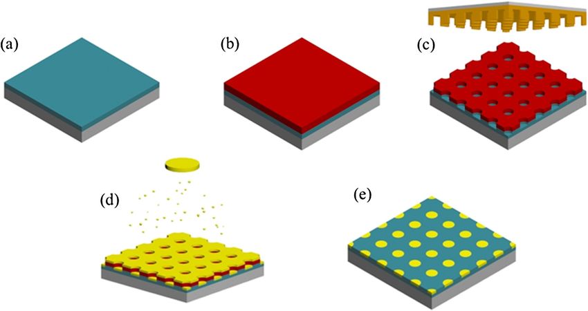
Choi et al.: Bilayer hybrid nanoimprinting method for fabricating embedded silver nanostructure arrays. . .

                                 5 mA∕cm2 ; however, the efficiencies can be increased by 13% by planarization of the device
                                 with multiple spin-coated layers of ZnO sol-gel.21 Alternatively, to reduce current leakage and
                                 enhance light extraction, multiple spin-coated layers and physical pressing of a higher refractive
                                 sol-gel oxide, TiO2 , can be used to fill in and smooth any “pillar”-like nanostructures on the glass
                                 substrate prior to deposition of the anode in OLED fabrication.22 In fact, if corrugated Ag nano-
                                 structures exceed a critical height, then the increase in efficiency attributable to the Ag nano-
                                 structures is offset by efficiency decreases attributable to a grating effect on the
                                 electroluminescence intensity and absorption.2 Thus, the corrugated nanopattern-endowed
                                 benefits must be balanced against effects such as light scattering and spectral absorptions.
                                     Similar effects have been observed when plasmonic metal structures have been incorporated
                                 into devices. Relevant previous studies have attempted to selectively infiltrate metal nanopar-
                                 ticles directly into nanopattern holes23,24 or have used a template stripping method.25–28 For
                                 example, the embedding of gold (Au) nanowires into an indium tin oxide anode layer was
                                 achieved by spin coating and surface energy-driven confinement of Au nanoparticles into
                                 the grating grooves.23 In this case, strong coupling between the waveguide mode and the plas-
                                 mon resonance nanowire in the transverse magnetic field mode could enhance direct-current
                                 conductivity and conferred unique optical behaviors. Furthermore, the template stripping
                                 method, initially developed by Frey et al.,25,26 has been shown to generate the same level of
                                 surface roughness of the embedded metal nanopattern surface as the surface of the target tem-
                                 plate for metal deposition. Accordingly, the corrugation levels of embedded metal nanopatterns
                                 should be optimized to achieve plasmonic resonance improvements in devices.
                                     Prior studies as referred above have significantly contributed to the understanding of the
                                 implications of using embedded metal nanostructures. However, in most cases, fabrication
                                 approaches have been complicated, requiring numerous process steps and leading to a lack
                                 of processability and reliability. In this study, a cost-effective and simple fabrication strategy
                                 for embedding metal nanoarrays was developed. Our method is based on bilayer hybrid NI
                                 [sequential thermal and ultraviolet (UV) NI in a single process step] followed by accessible
                                 metal lift-off. Transmittance spectra and photoluminescence (PL) enhancements observed in
                                 devices fabricated using our method were examined terms of the embedded nanopattern size
                                 in comparison with corresponding metal nanodot configurations.

                                 2 Experiments
                                 As shown in Figs. 1(a) and 1(b), the first step of fabrication is coating with UV-curable and
                                 thermally curable NI resists (UV cur 21, mr-I 7010E, MRT Inc., Korea). The UV resist was
                                 partially cured prior to deposition of the thermal resist to ensure that it would not be removed
                                 upon spin coating of the thermal resist. The UV resist was sufficiently precured to maintain its
                                 integrity while also achieving the minimal viscoelastic properties required for molding during
                                 the subsequent high-pressure imprinting. Because the UV and thermal NI resists had compatible
                                 chemistry and similar solvents, they tended to mix without precuring of the UV resist. Either UV
                                 exposure in an oxygen-free environment or vacuum plasma could be used for the precuring.
                                     Next, hard transparent stamps with protruding pillar arrays, which were replicated from Si
                                 master patterns, were applied in the NI step, as shown in Fig. 1(c). Three types of stamps were
                                 applied: a hexagonal array with 150-nm diameter and 300-nm-high nanopillars, a hexagonal
                                 array with 200-nm diameter and 250-nm-high nanopillars; and a hexagonal array with
                                 265-nm diameter and 270-nm-high nanopillars. Their pattern periodicity was identically
                                 twice of their diameters. The given pattern sizes were chosen to minimize the nonradiative
                                 PL decay.27 Bilayered resists were imprinted under increasing pressures up to ∼50 bar at
                                 150°C for 20 min in a vacuum chamber, and then subsequently exposed to a UV lamp (energy
                                 intensity ∼35.5 mW∕cm2 ) for 3 min while imprinted with the stamp. The quality of the pattern
                                 transferred to the underlying UV-curable resist was evaluated after mold release and removal of
                                 upper thermal resist layer. The thickness of the thermal resist was optimized to more effectively
                                 transfer the pattern to the underlying UV resist layer; the optimal thickness for the thermal resist
                                 layer was found to be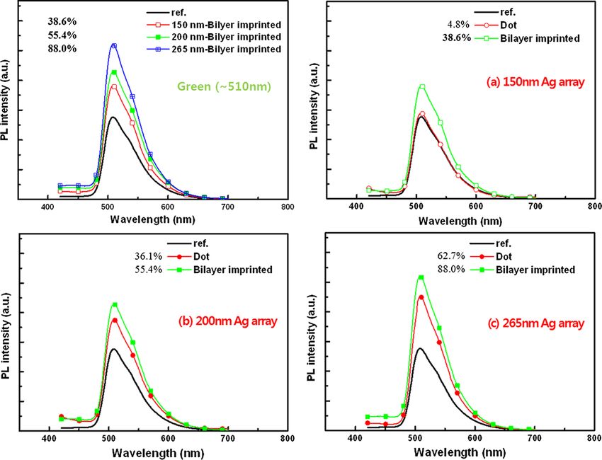
Choi et al.: Bilayer hybrid nanoimprinting method for fabricating embedded silver nanostructure arrays. . .

                                 Fig. 1 Schematic diagram of the bilayer hybrid nanoimprint (NI) process for fabricating embedded
                                 metal nanopatterns. The process consists of (a) coating the substrate with an ultraviolet
                                 (UV)-curable resist, (b) coating the substrate with a thermal NI resist, (c) thermal NI followed
                                 by UV exposure, (d) evaporation of Ag, and (e) lift-off of Ag metal and thermal NI resist.

                                 in-house electron-beam evaporator, as shown in Fig. 1(d), to fill the holes on the bottom side of
                                 the UV-cured resist layer. The Ag deposited on the tops and sidewalls of the imprinted holes on
                                 the upper thermal resist was then easily removed along with the thermal resist in acetone under
                                 ultrasonication for 5 min, as shown in Fig. 1(e). Thus, Ag remained only in the imprinted holes
                                 on the UV-cured resist, thereby completing the embedded Ag nanopattern configuration.
                                 Reference samples for comparison were made with protruding dot-shaped Ag nanopatterns.
                                 These counterpart samples were fabricated by Ag lift-off on the predefined NI patterns
                                 using lift-off resist and a Si-based etch mask material.15
                                     The transmittance spectra of the embedded Ag and protruding Ag nanodot samples were
                                 measured in the UV-visible wavelength range (NEOSYS-2000, SCINCSO Inc., Korea).
                                 Prior to the deposition of PL layer, a 20-nm oxide layer was deposited as a spacer on both
                                 the protruding Ag dot-shaped and embedded Ag samples to prevent quenching to eliminate
                                 PL quenching. Pre-existing native oxide should add, which was considered to be still in the
                                 optimum range (20 to 25 nm) of quenching-resistant thickness of oxide layer.29
                                     The PL materials used were green-emitting tris[2-(p-tolyl)pyridine] iridium (III) [IrðmppyÞ2 ]
                                 (EM Index Co., Seoul, Korea). The PL materials were dissolved in chlorobenzene, doped with
                                 polymethymethacrylate (PMMA), and spin-coated onto the oxide layer on the sample substrates. It
                                 was baked on a hotplate at 80°C for 20 min. The PL spectrum of IrðppyÞ3 complexes-doped
                                 PMMA films showed the excitation peak at 370-nm wavelength. The PL spectra were measured
                                 using a Hitachi F-4500 fluorescence (Tokyo, Japan) spectrophotometer focused at green emission
                                 to compare the different Ag configurations and to investigate the size dependence in combination
                                 with the transmittance spectra. The solid-state emission measurements were carried out by using
                                 each film supported on a quartz substrate that was mounted with front-face excitation at an angle of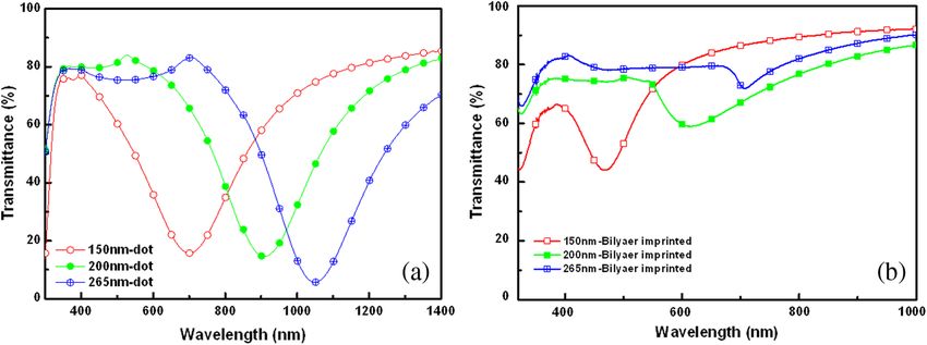
Choi et al.: Bilayer hybrid nanoimprinting method for fabricating embedded silver nanostructure arrays. . .

                                 Fig. 2 Scanning electron microscopy (SEM) images of the bilayer hybrid NI process correspond-
                                 ing to (a) the thermal NI and UV exposure step depicted in Figs. 1(c) and 1(b) the Ag evaporation
                                 step depicted in Fig. 1(d).

                                 Fig. 3 The SEM images of Ag hexagonal nanoarrays (a) protruding dot-shaped Ag nanopattern
                                 with 200-nm-diameter structures, and (b)–(d) the embedded configuration with 150-, 200-, and
                                 265-nm-diameter structures, respectively.

                                 Journal of Nanophotonics                              083089-4                                   Vol. 8, 2014

Downloaded From: https://www.spiedigitallibrary.org/journals/Journal-of-Nanophotonics on 21 Nov 2021
Terms of Use: https://www.spiedigitallibrary.org/terms-of-use
Choi et al.: Bilayer hybrid nanoimprinting method for fabricating embedded silver nanostructure arrays. . .
nanoarrays fabricated for three hole diameters (150, 200, and 265 nm) are presented in
Figs. 3(b)–3(d). The SEM image of a 200-nm-diameter protruding dot-shaped Ag nanoarray,
which was fabricated using metal lift-off assisted with a Si-based etch mask material and
lift-off resist to minimize the rabbit-ear side profile for the comparative study, is shown in
Fig. 3(a).
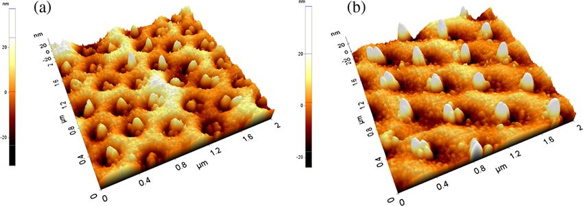
Figures 4(a) and 4(b) present atomic force microscopy (AFM) images of the Ag nanoarrays
with feature diameters greater than 150 nm. Figures 4(a) and 4(b) correspond to the nanoarrays
depicted in Figs. 3(c) and 3(d) above, respectively. An AFM image of the 150-nm nanoarray
[corresponding to the SEM image in Fig. 3(b)] is excluded because inaccurate measurement
deviations associated with the AFM tip size were observed for this specimen. The AFM images
for the 200- and 265-nm nanoarrays were qualitatively well matched to the SEM images. The
structures exhibited clear but slightly exaggerated profiles with pronounced edge waviness
around the imprinted holes. The stretched waviness of the imprinted hole surfaces on the
UV-cured resist and the ball-shaped silver dots inside the holes are expected to reduce the cor-
rugation period roughly by half, so-called the reduced pseudo-periodicity resulting from the
deformed pattern profile. In addition, the features in the embedded Ag nanoarrays were projected
more distinctly in the AFM images than in the SEM images because of scanning inaccuracy and
interface tolerances.
The different Ag nanoarray configurations resulted in different optical performance. Figure 5
shows the dependence of transmittance on the feature size for two given Ag surface configu-
rations. The transmittance fluctuated more in the protruding Ag nanodot-shaped samples
[Fig. 5(a)] than in the bilayer-imprinted embedded Ag nanoarray samples [Fig. 5(b)]. For
both shapes, the plasmonic peak wavelength was red shifted as the feature size increased. It
moved from 700 to 1050 nm in wavelength as the dot size increased from 150 to 265 nm.
Transmittances at the plasmonic extinction peak wavelength were greater for the embedded
Fig. 4 Atomic force microscopy profile images of embedded Ag nanoarrays with (a) 200- and
(b) 265-nm-diameter structures.
Fig. 5 Transmittance spectra of Ag nanoarrays with 150-, 200-, and 265-nm configurations:
(a) dot-shaped protruding Ag nanoarrays and (b) embedded Ag nanoarrays fabricated using
bilayer hybrid NI.
Journal of Nanophotonics 083089-5 Vol. 8, 2014
Downloaded From: https://www.spiedigitallibrary.org/journals/Journal-of-Nanophotonics on 21 Nov 2021
Terms of Use: https://www.spiedigitallibrary.org/terms-of-useChoi et al.: Bilayer hybrid nanoimprinting method for fabricating embedded silver nanostructure arrays. . .
Ag nanoarray than for the Ag dot-shaped nanoarray; the transmittance values were 15.7% and
5.7% for the Ag dot-shaped nanoarray with 150- and 265-nm features, respectively, and 44.1%
and 72% for the embedded Ag nanoarray with 150- and 265-nm features, respectively. Blue
shifts of the plasmonic extinction peak wavelength were observed in all of the embedded
Ag nanoarray samples for all pattern sizes. The blue shifts were attributed to the somewhat
wavy edge profiles between the imprinted holes and the silver inclusions, different materials
between the silver patterns, and more effective higher order diffractions that were not picked
up by our measurement scheme. However, scattering effects, particularly back-scattering,
seem to dominate the plasmonic extinctions obtained for the dot-shaped configurations
[Fig. 5(a)]; thus, it was conversely inferred that the decreased transmittance observed in the
embedded Ag configuration could be attributed to plasmonic absorptions [Fig. 5(b)].
The PL measurements as a function of configuration and pattern size are summarized in Fig. 6.
The structural configuration remarkably influenced the PL. For green-emitting PL materials, the
enhancement factor increased with the pattern size for the embedded Ag nanopattern samples
[Fig. 6(a)], although slight spectral mismatches still existed. Compared with the reference sample
with no Ag, the PL enhancements at an emitting wavelength of 510 nm were 38.6%, 55.4%, and
88.0% for nanoarrays with 150-, 200-, and 265-nm features, respectively. The embedded Ag nano-
array configurations exhibited even larger PL enhancements than the dot-shaped Ag nanoarrays for
all pattern sizes, as shown in Figs. 6(b)–6(d). The 150-nm dot-shaped Ag nanoarray resulted in a
4.8% enhancement compared with the reference sample with no Ag, whereas its embedded Ag
counterpart exhibited an enhancement of 38.6%, which corresponds to a relative PL enhancement
over the dot-shaped Ag nanoarray of ∼32.2%. The PL enhancements of the dot-shaped Ag nano-
arrays were 36.1% and 62.7% for the pattern sizes of 200 nm and 265 m, respectively, which even
increased up to 55.4% and 88.0% for their counterpart embedded Ag configurations with the
relative PL enhancement ratios of 14.2% and 15.6%, respectively.
Fig. 6 Photoluminescence (PL) enhancements with green-emitting PL materials [IrðmppyÞ3 ] on
SiOx-deposited silver-nanopatterned glass subtrates: (a) the dependence of PL on the size of
the embedded Ag nanoarray, and (b)–(d) comparisons of protruding dot-shaped Ag nanoarrays
(200-nm diameter) and embedded Ag nanoarrays with diameters of 150, 200, and 265 nm,
respectively.
Journal of Nanophotonics 083089-6 Vol. 8, 2014
Downloaded From: https://www.spiedigitallibrary.org/journals/Journal-of-Nanophotonics on 21 Nov 2021
Terms of Use: https://www.spiedigitallibrary.org/terms-of-useChoi et al.: Bilayer hybrid nanoimprinting method for fabricating embedded silver nanostructure arrays. . .
The larger PL enhancements for the Ag-embedded nanoarrays could be partially attributed to
decreased scattering loss observed in the transmittance measurements (Fig. 5), which might
result in a plasmonic field-driven increase in photon absorption in the PL layer. However,
the observed transmittance differences between the embedded and the dot shapes are trivial
for all the given pattern sizes in PL at the excitation wavelength of 510 nm. Hence, this
would not fully explain the much higher relative PL enhancements of the embedded Ag nano-
arrays. Thus, other phenomena must have also occurred. Higher order diffractive scattering
would have also caused more photons to be absorbed in the PL layer, which would have con-
tributed to an increase in PL for the embedded Ag nanoarrays compared with their counterpart
dot-shaped Ag nanoarrays, but this phenomenon was not detected in the transmittance measure-
ments. Instead, the blue shifted extinction peak wavelength may have more directly influenced
the relative PL improvements, facilitating the plasmonic resonance matching condition and
subsequently its near-field coupling to PL. At near the PL emitting wavelength, the surface plas-
monic field energy can be resonantly out-coupled to facilitate PL emissions through repetitive
charge generations and photon absorptions caused by the field intensification,30,31 and also the
embedded Ag nanopatterns may have scattered more of the near-field luminescence that would
have otherwise been trapped in the waveguide mode.
The increased photon absorptions and near-field plasmonic coupling efficiency would be the
major causes of the larger PL improvements for the embedded Ag configurations. The decreased
scattering loss, increased higher order diffractions, and blue shifting of the peak wavelength were
the most likely underlying related factors leading to the PL improvements. These effects were
more pronounced when Ag nanoarrays were embedded instead of protruding. The present study
was focused on the development of a new fabrication strategy for embedded Ag nanopatterns
and the exploration of their enhancement of plasmonic PL. Additional fundamental studies
aimed at better understanding the enhancement physics are suggested.
4 Conclusion
A bilayer hybrid NI method followed by silver lift-off was developed for the fabrication of
embedded Ag nanoarrays. In addition, the improved plasmonic-coupling effectiveness of
embedded Ag nanoarrays was investigated through PL measurements in comparison with refer-
ence samples with no silver and their counterpart protruding dot-shaped Ag nanoarray configu-
rations. The process was characterized by imprinting of the bilayer-deposited resist system
(including UV-curable and thermally curable resists), leaving the imprinted holes on the under-
lying UV resist available for subsequent Ag deposition. The top surface of the thermal resist
acted as a buffer layer for imprint pattern transfer to the underlying UV-curable resist and as
a sacrificial layer for subsequent metal lift-off. As an additional benefit, the Ag trapped in
the imprinted holes was more resistive to a swirling lift-off process using a wet chemical
bath than to conventional lift-off.
Transmittance and PL were measured for the embedded Ag nanoarrays and protruding Ag
dot-shaped nanoarrays with three different feature diameters as well as for reference samples
with no Ag. The plasmonic peak wavelength was blue shifted, and the scattering loss was
lower for the embedded Ag configuration than for the protruding Ag dot-shaped configuration.
PL enhancements compared with reference samples were observed for all samples containing Ag
nanoarrays; the observed enhancements were greater for the embedded Ag nanoarrays than for
the Ag dot-shaped nanoarrays. Relative PL enhancements of embedded Ag nanoarrays com-
pared with Ag dot-shaped nanoarrays were 32.2%, 14.2%, and 15.6% for 150-, 200-, and
265-nm pattern sizes, respectively. The largest relative PL enhancement for 150 nm can be
explained in a point of the spectral matching between the plasmonic extinction and the emitting
wavelength of the given green PL material. The gap between plasmonic extinction wavelength
and the emitting wavelength (510 nm) seems to be quite critical. It is smaller in the embedded
ones than in the dot-shaped ones. It reduced from 190 to 40 nm in the diameter of 150 nm, from
910 to 110 nm for 200 nm, and from 1050 to 710 nm for 265 nm. Hence, its highest rate (78.9%)
occurred for 150-nm pattern size, which probably leaded to the largest relative PL enhancement.
The effects of the metal nanostructure size on PL intensity have been investigated in Ref. 32.
Journal of Nanophotonics 083089-7 Vol. 8, 2014
Downloaded From: https://www.spiedigitallibrary.org/journals/Journal-of-Nanophotonics on 21 Nov 2021
Terms of Use: https://www.spiedigitallibrary.org/terms-of-useChoi et al.: Bilayer hybrid nanoimprinting method for fabricating embedded silver nanostructure arrays. . .
The PL enhancements were evaluated using transmittance spectra and discussed from the
view point of effective plasmonic near-field coupling efficiency and scatter-driven photon
absorption in PL layer. The embedded configuration was the most effective for extracting
the PL excitations and reducing the scattering loss. This study focused on presenting a new
fabrication method for fabrication of embedded Ag nanopatterns and exploration of their
enhancement of plasmonic PL. The presented bilayer hybrid NI method is simple and minimized
the process steps required for fabricating embedded Ag nanopatterns.
Acknowledgments
This research was supported by grants from the Basic Science Research Program (2011-
0028585) and the Global Frontier R&D program (2011-0031563), funded by the National
Research Foundation of Korea (NRF) under the Ministry of Education, Science, and
Technology. Dr. Jun-Hyuk Choi developed and planned the present approach, and contributed
to writing the paper. Mr Sang-Keun Sung contributed to metal evaporation and lift-offs. Mr
Chul-Hyun performed the fabrication of nanopatterns by hybrid nanoimprint. Mr Yeon-Ho
Jeong contributed to measuring photoluminescence and transmittance spectra. Dr. Joo-Yeon
Jeong designed mold patterns by simulations. Dr. Jun-Ho Jeong took responsibility for nano-
imprint mold fabrications. Dr. Eung-sug Lee contributed to preparing all material choices and
provided all valuable suggestions in the nanoimprint.
References
1. M. G. Kang et al., “Efficiency enhancement of organic solar cells using transparent plas-
monic Ag nanowire electrode,” Adv. Mater. 22(39), 4378–4383 (2010), http://dx.doi.org/10
.1002/adma.v22:39.
2. X. L. Zhang et al., “Grating amplitude effect on electroluminescence enhancement of
corrugated organic light-emitting devices,” Appl. Phys. Lett. 36(19), 3915–3917 (2011),
http://dx.doi.org/10.1364/OL.36.003915.
3. J. Feng and T. Okamoto, “Enhancement of electroluminescence through a two-dimensional
corrugated metal film by grating-induced surface-plasmon cross coupling,” Opt. Exp.
30(17), 2302–2304 (2005), http://dx.doi.org/10.1364/OL.30.002302.
4. V. Reboud et al., “Nanoimprinted plasmonic crystals for light extraction application,”
Microelectron. Eng. 87(5), 1367–1369 (2010), http://dx.doi.org/10.1016/j.mee.2009.12
.030.
5. J. Maria et al., “Optimization of 3D plasmonic crystal structures for refractive index
sensing,” J. Phys. Chem. C 113(24), 10493–10499 (2009), http://dx.doi.org/10.1021/
jp9024552.
6. J. Yao et al., “Seeing molecules by eye: surface plasmon resonance imaging at visible wave-
lengths with high spatial resolution and submonolayer sensitivity,” Angew. Chem. Inst. Ed.
120(27), 5091–5095 (2008), http://dx.doi.org/10.1002/anie.v47:27.
7. M. E. Stewart et al., “Quantitative multispectral biosensing and 1D imaging using quasi-3D
plasmonic crystals,” Proc. Natl. Acad. Sci. U. S. A. 103(46), 17143–17148 (2006), http://dx
.doi.org/10.1073/pnas.0606216103.
8. R. K. Gupta et al., “Enhancing charge-storage capacity of non-volatile memory devices
using template-directed assembly of gold nanoparticles,” Nanoscale 4(7), 2296–3000
(2012), http://dx.doi.org/10.1039/c2nr12134d.
9. D. K. Yun et al., “Fabrication of TiO 2 memristive arrays by Step and flash imprint lithography,”
J. Nanosci. Nanotechnol. 11(1), 696–700 (2011), http://dx.doi.org/10.1166/jnn.2011.3282.
10. B. Cui et al., “Fabrication of large area nanoprism arrays and their application for surface
enhanced Raman spectroscopy,” Nanotechnology 19(14), 145302 (2008), http://dx.doi.org/
10.1088/0957-4484/19/14/145302.
11. M. Singh et al., “Optical properties of d.c. magneto sputtered tantalum and titanium nano-
structure thin film metal hydrides,” Bull. Mater. Sci. 33(5), 569–573 (2010), http://dx.doi
.org/10.1007/s12034-010-0087-8.
Journal of Nanophotonics 083089-8 Vol. 8, 2014
Downloaded From: https://www.spiedigitallibrary.org/journals/Journal-of-Nanophotonics on 21 Nov 2021
Terms of Use: https://www.spiedigitallibrary.org/terms-of-useChoi et al.: Bilayer hybrid nanoimprinting method for fabricating embedded silver nanostructure arrays. . .
12. C. J. Ting, C. F. Chen, and C. J. Hsu, “Heat-insulation film with gold layer deposited on
antireflection subwavelength-structured surface,” Optik 121(20), 1877–1880 (2010), http://
dx.doi.org/10.1016/j.ijleo.2009.05.013.
13. E. U. Kim et al., “Templated assembly of metal nanoparticles in nanoimprinted patterns for
metal nanowire fabrication,” Nanotechnology 20(35), 355302 (2009), http://dx.doi.org/10
.1088/0957-4484/20/35/355302.
14. G. Xia, S. Wang, and S.-J. Jeong, “A universal approach for template-directed assembly of
ultrahigh density magnetic nanodot arrays,” Nanotechnology 21(48), 485302 (2010), http://
dx.doi.org/10.1088/0957-4484/21/48/485302.
15. K.-M. Lim et al., “Development of metal etch mask by single layer lift-off for silicon nitride
photonic crystals,” Microelectron. Eng. 88(6), 994–998 (2011), http://dx.doi.org/10.1016/j
.mee.2010.12.113.
16. F. De Angelis et al., “Emerging fabrication techniques for 3D nano-structuring in plasmonics and
single molecule studies,” Nanoscale 3(7), 2689–2696 (2011), http://dx.doi.org/10.1039/
c1nr10124b.
17. A. T. Hindmarch, D. E. Parkes, and A. W. Rushforth, “Fabrication of metallic magnetic
nanostructures by argon ion milling using a reversed-polarity planar magnetron ion source,”
Vacuum 86(10), 1600–1604 (2012), http://dx.doi.org/10.1016/j.vacuum.2012.02.019.
18. S. Kim et al., “Nanoimprinted plasmonic nanocavity arrays,” Opt. Exp. 21(13),
15081–15089 (2013), http://dx.doi.org/10.1364/OE.21.015081.
19. S. H. Jeon et al., “Ultraviolet nanoimprinted polymer nanostructure for organic light
emitting diode application,” Appl. Phys. Lett. 92(22), 223307 (2008), http://dx.doi.org/
10.1063/1.2939554.
20. K. Ishihara et al., “Organic light-emitting diodes with photonic crystals on glass substrate
fabricated by nanoimprint lithography,” Appl. Phys. Lett. 90(11), 111114 (2007), http://dx
.doi.org/10.1063/1.2713237.
21. H. H. Cho et al., “Solution-processed photonic crystals to enhance the light outcoupling
efficiency of organic light-emitting diodes,” Appl. Opt. 49(21), 4024–4028 (2010),
http://dx.doi.org/10.1364/AO.49.004024.
22. H. H. Cho et al., “Planarization of nanopatterned substrates using solution process to
enhance outcoupling efficiency of organic light-emitting diodes,” Curr. Appl. Phys. 10(4),
e139–e142 (2010), http://dx.doi.org/10.1016/j.cap.2010.08.027.
23. X. Zhang, B. Sun, and R. H. Friend, “Metallic photonic crystals based on solution-
processible gold nanoparticles,” Nano Lett. 6(4), 651–655 (2006), http://dx.doi.org/10
.1021/nl052361o.
24. B. Yang et al., “Electrochemical deposition of silver nanoparticle arrays with tunable
density,” Langmuir 25(1), 55–58 (2009), http://dx.doi.org/10.1021/la803559c.
25. W. Frey, C. K. Woods, and A. Chilkoti, “Ultraflat nanosphere lithography: a new method to
fabricate flat nanostructures,” Adv. Mater. 12(20), 1515–1519 (2000), http://dx.doi.org/10
.1002/(ISSN)1521-4095.
26. B. Jung and W. Frey, “Large-scale ultraflat nanopatterned surfaces without template residues,”
Nanotechnology 19(14), 145303 (2008), http://dx.doi.org/10.1088/0957-4484/19/14/145303.
27. P. Viste et al., “Enhancement and quenching regimes in metal-semiconductor hybrid optical
nanosources,” ACS Nano 4(2), 759–764 (2010), http://dx.doi.org/10.1021/nn901294d.
28. G. F. Walsh and L. D. Negro, “Engineering plasmon-enhanced Au light emission with planar
arrays of nanoparticles,” Nano Lett. 13(2), 786–792 (2013), http://dx.doi.org/10.1021/
nl304523v.
29. K. Ray et al., “Distance dependence of surface plasmon-coupled emission observed using
Langmuir-Blodgett films,” Appl. Phys. Lett. 90(25), 251116 (2007), http://dx.doi.org/10
.1063/1.2751125.
30. Y. Wang et al., “Radiative rate enhancements in ensembles of hybrid metal-semiconductor
nanostructures,” Phys. Rev. Lett. 102(16), 163001 (2009), http://dx.doi.org/10.1103/
PhysRevLett.102.163001.
31. F. Yan and X. W. Sun, “A plasmonically enhanced charge generation layer for tandem
organic light emitting device,” Appl. Phys. Lett. 102(4), 043303 (2013), http://dx.doi
.org/10.1063/1.4789979.
Journal of Nanophotonics 083089-9 Vol. 8, 2014
Downloaded From: https://www.spiedigitallibrary.org/journals/Journal-of-Nanophotonics on 21 Nov 2021
Terms of Use: https://www.spiedigitallibrary.org/terms-of-useChoi et al.: Bilayer hybrid nanoimprinting method for fabricating embedded silver nanostructure arrays. . .
32. A. Simo et al., “Formation mechanism of silver nanoparticles stabilized in glassy matrics,”
J. Amer. Chem. Soc. 134(45), 18824–18833 (2012), http://dx.doi.org/10.1021/ja309034n.
Jun-Hyuk Choi received his PhD in 2000 from the Department of Mechanical Engineering,
University of California at Berkeley. He joined KIMM (Korea Institute of Machinery and
Materials) in Daejeon, South Korea, in 2003. At present, he is a principle researcher in
KIMM. Also, he is an associate editor in International Journal of Precision Engineering
and Manufacturing and Trans. Kor. Soc. Mech. Eng. C. His research interests include nano-
imprint, metal nanopatterning and nanostructures-based photonic, and plasmonic applications.
Sang-Keun Sung received his MS degree in 2011 from the department of physics in Chungnam
National University, Daejeon, South Korea. He joined in the department of nanomanufacturing
technology of KIMM (Korea Institute of Machinery and Materials) in 2011, and is presently an
assistant researcher in KIMM. His research interests include nanopatterning using nanoimprint
and its applications to plasmonic optoelectronics.
Chul-Hyun Kim received his MS in 2011 from the department of display engineering, Busan
National University, South Korea. He majored in the materials and fabrication for organic light
emitting devices. He was an assistant researcher in KIMM (Korea Institute of Machinery and
Materials) in Daejeon, South Korea, from 2011 to 2013. Then he worked in hybrid nanoimprint
and its application to plasmonic OLED. He joined LG chemicals in 2013. Now, he is a staff
engineer in the division of organic lighting.
Yeon-Ho Jung received his BS degree in 2012 from the Department of Mathematics in Korea
University, South Korea. He majored in both mathematics and industrial engineering. He is pres-
ently enrolled in the University of Science and Technology for his graduate program. Coupled
with this graduate research program, he is affiliated with KIMM (Korea Institute of Machinery
and Materials). His research areas include nanopatterning using nanoimprint and nanostructure-
driven color imaging.
Joo-Yun Jung received his PhD in 2010 from the department of electrical and computer engi-
neering, University of Texas at Austin. He joined KIMM (Korea Institute of Machinery and
Materials) in Daejeon, South Korea, in 2010. At present, he is a senior researcher in
KIMM. His research interests include nanoimprint, metamaterials and nanostructures-based
photonic, and plasmonic applications.
Jun-Ho Jeong received his undergraduate training at Hanyang University (BS 1990) and his MS
at KAIST where he completed his PhD in mechanical engineering in 1998. He is currently a
principle search scientist at KIMM. His research interests include nanofabrication, especially
nanoimprint lithography (NIL) and nanofluidics.
Eung-Sug Lee is presently a vice president of KIMM as a tenured principle researcher. He used
to serve as a director of the Division of Nano and Convergence Technology in the National
Research Foundation of Korea from 2009 to 2011. He has been credited with more than seventy
patents, and a contributing author of thirties SCI publications during the last 5 years in the field
of nanoimprint, plasmonic nanostructure, and various nanopattern-based optoelectronics.
Journal of Nanophotonics 083089-10 Vol. 8, 2014
Downloaded From: https://www.spiedigitallibrary.org/journals/Journal-of-Nanophotonics on 21 Nov 2021
Terms of Use: https://www.spiedigitallibrary.org/terms-of-useYou can also read