C2000 Piccolo 1-Day Workshop - Workshop Guide and Lab Manual - Technical Training
←
→
Page content transcription
If your browser does not render page correctly, please read the page content below
C2000™ Piccolo™ 1-Day Workshop
               Workshop Guide and Lab Manual

F28xPodw
Revision 1.1
October 2009
                                   Technical Training
                                     Organization
Workshop Topics

Important Notice
      Texas Instruments and its subsidiaries (TI) reserve the right to make changes to their products or to
      discontinue any product or service without notice, and advise customers to obtain the latest version of
      relevant information to verify, before placing orders, that information being relied on is current and
      complete. All products are sold subject to the terms and conditions of sale supplied at the time of order
      acknowledgment, including those pertaining to warranty, patent infringement, and limitation of liability.

      TI warrants performance of its semiconductor products to the specifications applicable at the time of sale in
      accordance with TI’s standard warranty. Testing and other quality control techniques are utilized to the
      extent TI deems necessary to support this warranty. Specific testing of all parameters of each device is not
      necessarily performed, except those mandated by government requirements.

      Customers are responsible for their applications using TI components.

      In order to minimize risks associated with the customer’s applications, adequate design and operating
      safeguards must be provided by the customer to minimize inherent or procedural hazards.

      TI assumes no liability for applications assistance or customer product design. TI does not warrant or
      represent that any license, either express or implied, is granted under any patent right, copyright, mask
      work right, or other intellectual property right of TI covering or relating to any combination, machine, or
      process in which such semiconductor products or services might be or are used. TI’s publication of
      information regarding any third party’s products or services does not constitute TI’s approval, warranty or
      endorsement thereof.

      Copyright © 2009 Texas Instruments Incorporated

      Revision History
      April 2009 – Revision 1.0
      October 2009 – Revision 1.1

      Mailing Address
      Texas Instruments
      Training Technical Organization
      7839 Churchill Way
      M/S 3984
      Dallas, Texas 75251-1903

2                                                                              C2000 Piccolo 1-Day Workshop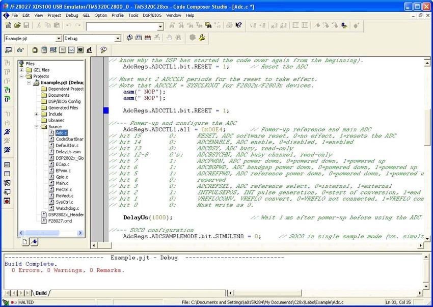
Workshop Topics

Workshop Topics
         Workshop Topics.........................................................................................................................................3
         Workshop Introduction ...............................................................................................................................4
         Architecture Overview ................................................................................................................................8
         Programming Development Environment.................................................................................................10
           Code Composer Studio.........................................................................................................................10
           Linking Sections in Memory ................................................................................................................12
         Lab 1: Linker Command File....................................................................................................................15
         Peripheral Register Header Files .............................................................................................................19
         Reset, Interrupts and System Initialization ...............................................................................................26
           Reset .....................................................................................................................................................26
           Interrupts ..............................................................................................................................................28
           Peripheral Interrupt Expansion (PIE) ...................................................................................................30
           Oscillator / PLL Clock Module ............................................................................................................32
           Watchdog Timer Module......................................................................................................................33
           GPIO.....................................................................................................................................................34
         Lab 2: System Initialization ......................................................................................................................36
         Control Peripherals ..................................................................................................................................40
           ADC Module ........................................................................................................................................40
           Pulse Width Modulation.......................................................................................................................42
           ePWM...................................................................................................................................................43
           eCAP ....................................................................................................................................................56
           eQEP.....................................................................................................................................................57
         Lab 3: Control Peripherals.......................................................................................................................59
         Flash Programming ..................................................................................................................................65
           Flash Programming Basics ...................................................................................................................65
           Programming Utilities and CCS Plug-in ..............................................................................................66
           Code Security Module and Password ...................................................................................................67
         Lab 4: Programming the Flash.................................................................................................................69
         The Next Step….........................................................................................................................................76
           Training ................................................................................................................................................76
           Development Tools...............................................................................................................................77
           Development Support ...........................................................................................................................79

C2000 Piccolo 1-Day Workshop                                                                                                                                         3
Workshop Introduction
Workshop Introduction
C2000™ Piccolo™ 1-Day Workshop
Texas Instruments
Technical Training
T TO
Technical Training
Organization C2000 and Piccolo are trademarks of Texas Instruments. Copyright © 2009 Texas Instruments. All rights reserved.
C2000 Piccolo 1-Day Workshop Outline
Workshop Introduction
Architecture Overview
Programming Development Environment
Lab: Linker command file
Peripheral Register Header Files
Reset, Interrupts and System Initialization
Lab: Watchdog and interrupts
Control Peripherals
Lab: Generate and graph a PWM waveform
Flash Programming
Lab: Run the code from flash memory
The Next Step…
4 C2000 Piccolo 1-Day Workshop
Workshop Introduction
Introductions
Name
Company
Project Responsibilities
Microcontroller Experience
TMS320 Processor Experience
Hardware / Software - Assembly / C
Interests
C2000 Portfolio Expanding with
Price/Performance Optimized Derivatives
High-end
High-Precision Control Derivatives
F2834x
300 MIPS
Control Performance
F2833x/23x
150 MIPS
F281x
Multi-Function, 150 MIPS
Appliance & F280x/xx F2803x/2x
100 MIPS 60 MIPS
Consumer Control
F24xx
40 MIPS Cost
optimized
versions
C2000 Piccolo 1-Day Workshop 5
Workshop Introduction

                                Broad C2000 Application Base

                                        Renewable                     Telecom                   AC Drives, Industrial
                                         Energy                     Digital Power                & Consumer Motor
                                        Generation                                                    Control

                                      Automotive
                                    Radar, Electric
                                    Power Steering                                                      Power Line
                                    & Digital Power                                                   Communications

                                                                                                      LED Lighting
                                                              Consumer,
                                                               Medical &
                                                             Non-traditional

                  C2000 Piccolo™ Microcontroller Family
                                                         F2802x / F2803x
                                      Flash     RAM              Analog       ADC*           PWM          C Q
                              MHz                        CLA                                              A E Communication Ports
                                      (x16)     (x16)            Comp*        (ch)          / (HR)*       P P
                  F28020       40     16Kw      3Kw       No       1/2        7 / 13         8 (0)        1    0         SPI, SCI, I2C
                  F28021       40     32Kw      5Kw       No       1/2        7 / 13         8 (0)        1    0         SPI, SCI, I2C
                  F28022       40     16Kw      6Kw       No       1/2        7 / 13         8 (4)        1    0         SPI, SCI, I2C
                  F28023       40     32Kw      6Kw       No       1/2        7 / 13         8 (4)        1    0         SPI, SCI, I2C
                  F28026       60     16Kw      6Kw       No       1/2        7 / 13         8 (4)        1    0         SPI, SCI, I2C
                  F28027       60     32Kw      6Kw       No       1/2        7 / 13         8 (4)        1    0         SPI, SCI, I2C

                  F28032       60     32Kw     10Kw       No         3       14 / 16     12(6) / 14(7)    1    1   SPI,SCI,I2C,LIN,eCAN
                  F28033       60     32Kw     10Kw      Yes         3       14 / 16     12(6) / 14(7)    1    1   SPI,SCI,I2C,LIN,eCAN
                  F28034       60     64Kw     10Kw       No         3       14 / 16     12(6) / 14(7)    1    1   SPI,SCI,I2C,LIN,eCAN
                  F28035       60     64Kw     10Kw      Yes         3       14 / 16     12(6) / 14(7)    1    1   SPI,SCI,I2C,LIN,eCAN
                  * number dependent on package type: F2802x – 38/48 pins, F2803x – 64/80 pins

                   • All devices have VREG, POR/BOR, Watchdog, OTP, CPU Timers

                For details and information on other C2000 family members refer to the “Embedded Proc essing Guide” and specific “Data Manuals”

6                                                                                                          C2000 Piccolo 1-Day Workshop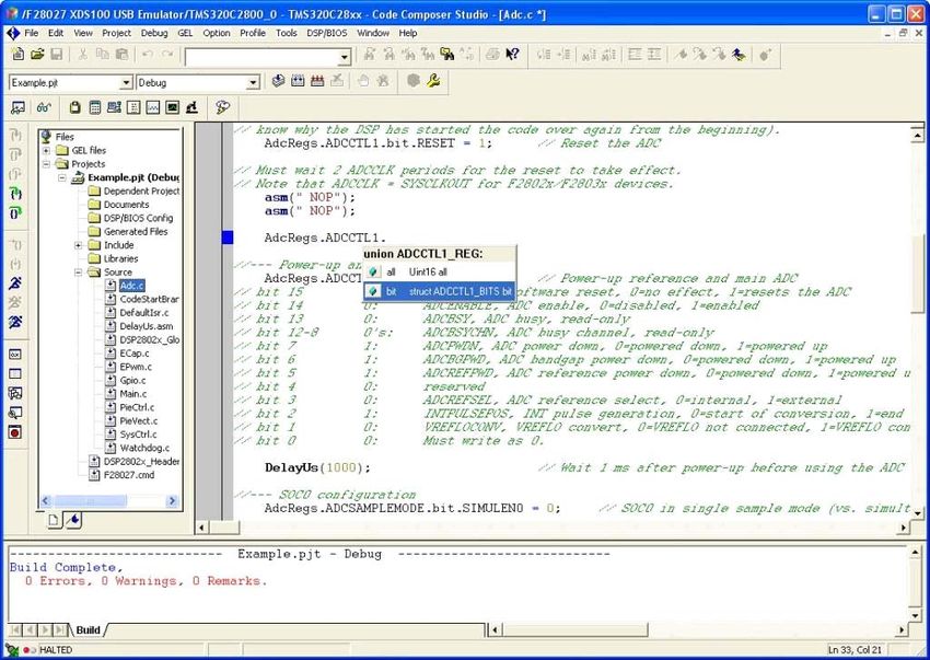
Workshop Introduction

                               Piccolo™ ControlSTICK

                                LED LD1        LED LD2     TMS320F28027
                                 (Power)       (GPIO34)    48-Pin Package

                               USB JTAG          On-board USB     Peripheral
                           Interface & Power    JTAG Emulation    Header Pins

C2000 Piccolo 1-Day Workshop                                                                   7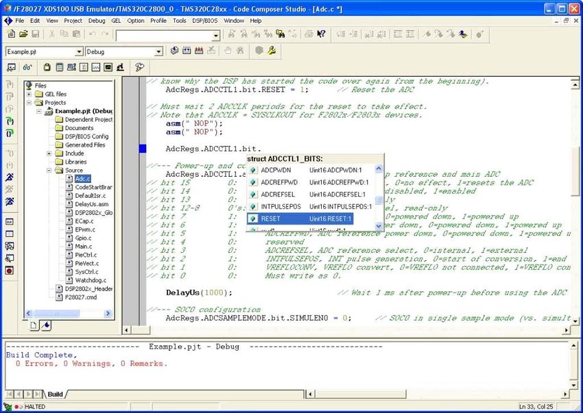
Architecture Overview

Architecture Overview
                          TMS320F2802x/3x Block Diagram
                                                      Program Bus
                                                                                                        ePWM

                                                                           Boot                          eCAP
                                    Sectored              RAM
                                                                           ROM
                                      Flash                                                             eQEP
                                                                 CLA Bus
                                                                                                      12-bit ADC

                                                                                                      Watchdog

                                                                                PIE
                                   32-bit              R-M-W                 Interrupt                CAN 2.0B
                                            32x32 bit                        Manager
                                  Auxiliary            Atomic         CLA
                                            Multiplier                                                   I2C
                                  Registers             ALU
                                                                                  3
                 Real-Time                                                                               SCI
                                                                              32-bit
                   JTAG                    Register Bus                       Timers                     SPI
                 Emulation                       CPU
                                                                                                            LIN
                                                           Data Bus
                                                                                                         GPIO
                        Available only on TMS320F2803x devices: CLA, QEP, CAN, LIN

                               TMS320F28027 Memory Map
                                              Data     Program
                             0x000000
                                           M0 SARAM (1Kw)
                             0x000400                                 0x3D7C80
                                           M1 SARAM (1Kw)                             ADC / OSC cal. data
                             0x000800                                 0x3D8000
                                                                                           reserved
                             0x000D00   PIE Vectors
                                                                      0x3F0000
                                          (256 w )
                             0x000E00              reserved                             FLASH (32Kw)
                                      PF 0 (6Kw)
                             0x002000                                 0x3F7FF8
                                                                                        PASSWORDS (8w)
                             0x006000                                 0x3F8000
                                      PF 1 (4Kw)                                       L0 SARAM (4Kw)
                             0x007000                                 0x3F9000
                                      PF 2 (4Kw)                                           reserved
                             0x008000                                 0x3FE000
                                        L0 SARAM (4Kw)                                 Boot ROM (8Kw)
                             0x009000
                                             reserved                 0x3FFFC0
                             0x3D7800                                 0x3FFFFF         BROM Vectors (64w)
                                         User OTP (1Kw)
                             0x3D7C00                                                   Data     Program
                                             reserved
                             0x3D7C80
                                                                                       Dual Mapped: L0

                                                                                        CSM Protected:
                                                                                            L0, OTP
                                                                                       FLASH, ADC CAL,
                                                                                       Flash Regs in PF0

8                                                                                         C2000 Piccolo 1-Day Workshop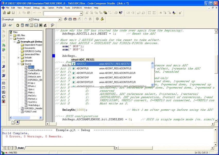
Architecture Overview
F28x Fast Interrupt Response Manager
96 dedicated PIE
vectors
PIE module
No software decision
Peripheral Interrupts 12x8 = 96
For 96 28x CPU Interrupt logic
interrupts
making required
INT1 to
Direct access to RAM INT12
vectors 96 12 interrupts IFR IER
28x
PIE INTM CPU
Auto flags update Register
Concurrent auto Map
context save
Auto Context Save
T ST0
AH AL
PH PL
AR1 (L) AR0 (L)
DP ST1
DBSTAT IER
PC(msw) PC(lsw)
C2000 Piccolo 1-Day Workshop 9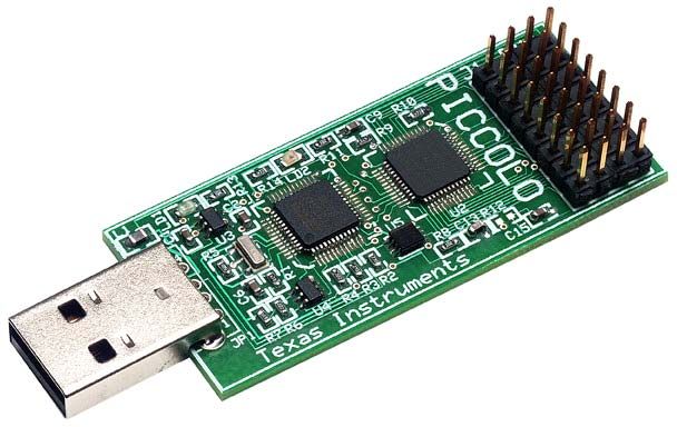
Programming Development Environment
Programming Development Environment
Code Composer Studio
Code Composer Studio: IDE
Integrates: edit, code generation,
and debug
Single-click access using buttons
Powerful graphing/profiling tools
Automated tasks using GEL scripts
and CCS scripting
Built-in access to BIOS functions
Supports TI and 3 rd party plug-ins
The CCS Project
Project (.pjt) files contain:
List of files:
Source (C, assembly)
Libraries
DSP/BIOS configuration file
Linker command files
Project settings:
Build options (compiler,
Linker, assembler, and
DSP/BIOS)
Build configurations
10 C2000 Piccolo 1-Day WorkshopProgramming Development Environment
Build Options GUI - Compiler
GUI has 8 pages of categories for code
generation tools
Controls many aspects of the build process,
such as:
Optimization level
Target device
Compiler/assembly/link options
Build Options GUI - Linker
GUI has 3 categories
for linking
Specify various link
options
.\Debug
means the directory
called Debug one
level below the .pjt
file directory
$(Proj_dir)\Debug
is an equivalent
expression
C2000 Piccolo 1-Day Workshop 11Programming Development Environment
Linking Sections in Memory
Sections
Global vars (.ebss) Init values (.cinit)
All code consists of
int x = 2; different parts called
int y = 7; sections
All default section
names begin with “.”
void main(void) The compiler has
{ default section
names for initialized
long z; and uninitialized
z = x + y; sections
}
Local vars (.stack) Code (.text)
Compiler Section Names
Initialized Sections
Name Description Link Location
.text code FLASH
.cinit initialization values for FLASH
global and static variables
.econst constants (e.g. const int k = 3;) FLASH
.switch tables for switch statements FLASH
.pinit tables for global constructors (C++) FLASH
Uninitialized Sections
Name Description Link Location
.ebss global and static variables RAM
.stack stack space low 64Kw RAM
.esysmem memory for far malloc functions RAM
Note: During development initialized sections could be linked to RAM since
the emulator can be used to load the RAM
12 C2000 Piccolo 1-Day WorkshopProgramming Development Environment
Placing Sections in Memory
Memory
Sections
0x00 0000 M0SARAM
(0x400)
.ebss
0x00 0400 M1SARAM
(0x400)
.stack
0x3F 0000 FLASH .cinit
(0x8000)
.text
Linking
z Memory description
z How to place s/w into h/w
Link.cmd
.obj Linker .out
.map
C2000 Piccolo 1-Day Workshop 13Programming Development Environment
Linker Command File
MEMORY
{
PAGE 0: /* Program Memory */
FLASH: origin = 0x3F0000, length = 0x8000
PAGE 1: /* Data Memory */
M0SARAM: origin = 0x000000, length = 0x400
M1SARAM: origin = 0x000400, length = 0x400
}
SECTIONS
{
.text:> FLASH PAGE = 0
.ebss:> M0SARAM PAGE = 1
.cinit:> FLASH PAGE = 0
.stack:> M1SARAM PAGE = 1
}
14 C2000 Piccolo 1-Day WorkshopLab 1: Linker Command File
Lab 1: Linker Command File
¾ Objective
Use a linker command file to link the C program file (Lab1.c) into the system described below.
Lab 1: Linker Command File
Memory 0x00 0000 M0SARAM
(0x400)
on-chip
0x00 0400 M1SARAM
memory
(0x400)
0x00 8000 L0SARAM
F28027 (0x1000)
System Description:
• TMS320F28027
• All internal RAM
blocks allocated
Placement of Sections:
• .text into RAM Block L0SARAM on PAGE 0 (program memory)
• .cinit into RAM Block L0SARAM on PAGE 0 (program memory)
• .ebss into RAM Block M0SARAM on PAGE 1 (data memory)
• .stack into RAM Block M1SARAM on PAGE 1 (data memory)
System Description
• TMS320F28027
• All internal RAM blocks allocated
Placement of Sections:
• .text into RAM Block L0SARAM on PAGE 0 (program memory)
• .cinit into RAM Block L0SARAM on PAGE 0 (program memory)
• .ebss into RAM Block M0SARAM on PAGE 1 (data memory)
• .stack into RAM Block M1SARAM on PAGE 1 (data memory)
¾ Procedure
Open a Project
1. Double click on the Code Composer Studio icon on the desktop. Maximize Code
Composer Studio to fill your screen. Code Composer Studio has a Connect/Disconnect
feature which allows the target to be dynamically connected and disconnected. This will
reset the JTAG link and also enable “hot swapping” a target board.
C2000 Piccolo 1-Day Workshop 15Lab 1: Linker Command File
2. Connect to the target.
Click: Debug Æ Connect
The menu bar (at the top) lists File ... Help. Note the horizontal tool bar below the menu
bar and the vertical tool bar on the left-hand side. The window on the left is the project
window and the large right-hand window is your workspace.
3. A project contains all the files you will need to develop an executable output file (.out)
which can be run on the MCU hardware. A project named Lab1.pjt has been created
for this lab. Open the project by clicking:
Project Æ Open…
and look in C:\C28x\LABS\LAB1. This .pjt file will invoke all the necessary tools
(compiler, assembler, linker) to build the project. It will also create a debug folder that
will hold immediate output files.
4. In the project window on the left, click the plus sign (+) to the left of Project. Now,
click on the plus sign next to Lab1.pjt. Notice that the Lab1.cmd file is listed.
5. Click on the plus sign next to Source to see the current source file list (i.e. Lab1.c).
A test file named Lab1.c has been added to the project. This file will be used in this
exercise to demonstrate some features of Code Composer Studio.
Project Build Options
6. There are numerous build options in the project. The default option settings are sufficient
for getting started. We will inspect a couple of the default linker options at this time.
Click: Project Æ Build Options…
7. Select the Linker tab. Notice that .out and .map files are being created. The .out file is
the executable code that will be loaded into the MCU. The .map file will contain a linker
report showing memory usage and section addresses in memory. The Stack Size has
been set to 0x200.
8. Select OK and the Build Options window will close.
Linker Command File – Lab1.cmd
9. Open and inspect Lab1.cmd by double clicking on the filename in the project window.
Notice that the Memory{} declaration describes the system memory shown on the
“Lab1: Linker Command File” slide in the objective section of this lab exercise.
Memory block L0SARAM has been placed in program memory on page 0, and the other
memory blocks have been placed in data memory on page 1.
10. In the Sections{} area notice that the sections defined on the slide have been “linked”
into the appropriate memories. Also, notice that a section called .reset has been allocated.
The .reset section is part of the rts2800_ml.lib, and is not needed. By putting the TYPE =
16 C2000 Piccolo 1-Day WorkshopLab 1: Linker Command File
DSECT modifier after its allocation, the linker will ignore this section and not allocate it.
Close the inspected file.
Build and Load the Project
11. The top four buttons on the horizontal toolbar control code generation. Hover your
mouse over each button as you read the following descriptions:
Button Name Description
1 Compile File Compile, assemble the current open file
2 Incremental Build Compile, assemble only changed files, then link
3 Rebuild All Compile, assemble all files, then link
4 Stop Build Stop code generation
12. Code Composer Studio can automatically load the output file after a successful build. On
the menu bar click: Option Æ Customize… and select the
“Program/Project/CIO” tab, then check “Load Program After Build”.
Also, Code Composer Studio can automatically connect to the target when started. Select
the “Debug Properties” tab, check “Connect to the target at
startup”, then click OK.
13. Click the “Build” button and watch the tools run in the build window. Check for
errors (we have deliberately put an error in Lab1.c). When you get an error, scroll the
build window at the bottom of the Code Composer Studio screen until you see the error
message (in red), and simply double-click the error message. The editor will
automatically open the source file containing the error, and position the mouse cursor at
the correct code line.
14. Fix the error by adding a semicolon at the end of the "z = x + y" statement. For
future knowlege, realize that a single code error can sometimes generate multiple error
messages at build time. This was not the case here.
15. Rebuild the project (there should be no errors this time). The output file should
automatically load. The Program Counter should be pointing to _c_int00 in the
Disassembly Window.
16. Under Debug on the menu bar click “Go Main”. This will run through the
C-environment initialization routine and stop at main() in Lab1.c.
Debug Enviroment Windows
It is standard debug practice to watch local and global variables while debugging code. There
are various methods for doing this in Code Composer Studio. We will examine two of them
here: memory windows, and watch windows.
17. Open a memory window to view the global variable “z”.
Click: View Æ Memory… on the menu bar.
C2000 Piccolo 1-Day Workshop 17Lab 1: Linker Command File
Type “&z” into the address field and then enter. Note that you must use the ampersand
(meaning “address of”) when using a symbol in a memory window address box. Also
note that Code Composer Studio is case sensitive.
Set the properties format to “Hex 16 Bit – TI style” at the bottom of the window. This
will give you more viewable data in the window. You can change the contents of any
address in the memory window by double-clicking on its value. This is useful during
debug.
18. Open the watch window to view the local variables x and y.
Click: View Æ Watch Window on the menu bar.
Click the “Watch Locals” tab and notice that the local variables x and y are already
present. The watch window will always contain the local variables for the code function
currently being executed.
(Note that local variables actually live on the stack. You can also view local variables in
a memory window by setting the address to “SP” after the code function has been
entered).
19. We can also add global variables to the watch window if desired. Let's add the global
variable “z”.
Click the “Watch 1” tab at the bottom of the watch window. In the empty box in the
“Name” column, type “z” and then enter. An ampersand is not used here. The watch
window knows you are specifying a symbol.
Check that the watch window and memory window both report the same value for “z”.
Trying changing the value in one window, and notice that the value also changes in the
other window.
Single-stepping the Code
20. Click the “Watch Locals” tab at the bottom of the watch window. Single-step through
main() by using the key (or you can use the Single Step button on the
vertical toolbar). Check to see if the program is working as expected. What is the value
for “z” when you get to the end of the program?
End of Exercise
18 C2000 Piccolo 1-Day WorkshopPeripheral Register Header Files
Peripheral Register Header Files
Traditional Approach to C Coding
#define ADCCTL1 (volatile unsigned int *)0x00007100
...
void main(void)
{
*ADCCTL1 = 0x1234; //write entire register
*ADCCTL1 |= 0x4000; //enable ADC module
}
Advantages - Simple, fast and easy to type
- Variable names exactly match register names (easy
to remember)
Disadvantages - Requires individual masks to be generated to
manipulate individual bits
- Cannot easily display bit fields in Watch window
- Will generate less efficient code in many cases
Structure Approach to C Coding
void main(void)
{
AdcRegs.ADCCTL1.all = 0x1234; //write entire register
AdcRegs.ADCCTL1.bit.ADCENABLE = 1; //enable ADC module
}
Advantages - Easy to manipulate individual bits.
- Watch window is amazing! (next slide)
- Generates most efficient code (on C28x)
Disadvantages - Can be difficult to remember the structure names
(Editor Auto Complete feature to the rescue!)
- More to type (again, Editor Auto Complete feature
to the rescue)
C2000 Piccolo 1-Day Workshop 19Peripheral Register Header Files
The CCS Watch Window using #define
The CCS Watch Window using Structures
20 C2000 Piccolo 1-Day WorkshopPeripheral Register Header Files
Structure Naming Conventions
The DSP2802x header files define:
All of the peripheral structures
All of the register names
All of the bit field names
All of the register addresses
PeripheralName.RegisterName.all // Access full 16 or 32-bit register
PeripheralName.RegisterName.half.LSW // Access low 16-bits of 32-bit register
PeripheralName.RegisterName.half.MSW // Access high 16-bits of 32-bit register
PeripheralName.RegisterName.bit.FieldName // Access specified bit fields of register
Notes: [1] “PeripheralName” are assigned by TI and found in the DSP2802x header files.
They are a combination of capital and small letters (i.e. CpuTimer0Regs).
[2] “RegisterName” are the same names as used in the data sheet.
They are always in capital letters (i.e. TCR, TIM, TPR,..).
[3] “FieldName” are the same names as used in the data sheet.
They are always in capital letters (i.e. POL, TOG, TSS,..).
Editor Auto Complete to the Rescue!
C2000 Piccolo 1-Day Workshop 21Peripheral Register Header Files
DSP2802x Header File Package
(http://www.ti.com, literature # SPRC832)
Contains everything needed to use the
structure approach
Defines all peripheral register bits and
register addresses
Header file package includes:
\DSP2802x_headers\include Æ .h files
\DSP2802x_headers\cmd Æ linker .cmd files
\DSP2802x_headers\gel Æ .gel files for CCS
\DSP2802x_examples Æ CCS3 examples
\DSP2802x_examples_ccsv4 Æ CCS4 examples
\doc Æ documentation
Peripheral Structure .h files (1 of 2)
Contain bits field structure definitions for each peripheral register
DSP2802x_Adc.h
// ADC Individual Register Bit Definitions:
struct ADCCTL1_BITS { // bits description
Uint16 TEMPCONV:1; // 0 Temperature sensor connection
Uint16 VREFLOCONV:1; // 1 VSSA connection
Your C-source file (e.g., Adc.c) Uint16 INTPULSEPOS:1; // 2 INT pulse generation control
Uint16 ADCREFSEL:1; // 3 Internal/external reference select
#include "DSP2802x_Device.h"
Uint16 rsvd1:1; // 4 reserved
Uint16 ADCREFPWD:1; // 5 Reference buffers powerdown
Void InitAdc(void)
Uint16 ADCBGPWD:1; // 6 ADC bandgap powerdow n
{
Uint16 ADCPWDN:1; // 7 ADC powerdown
/* Reset the ADC m odule */
Uint16 ADCBSYCHN:5; // 12:8 ADC busy on a channel
AdcRegs.ADCCTL1.bit.RESET = 1;
Uint16 ADCBSY:1; // 13 ADC busy signal
Uint16 ADCENABLE:1; // 14 ADC enable
/* configure the ADC register */
Uint16 RESET:1; // 15 ADC master reset
AdcRegs.ADCCTL1.all = 0x00E4;
};
};
// Allow access to the bit fields or entire register:
union ADCCTL1_REG {
Uint16 all;
struct ADCCTL1_BITS bit;
};
// ADC External References & Function Declarations:
extern volatile struct ADC_REGS AdcRegs;
22 C2000 Piccolo 1-Day WorkshopPeripheral Register Header Files
Peripheral Structure .h files (2 of 2)
The header file package contains a .h file
for each peripheral in the device
DSP2802x_Adc.h DSP2802x_BootVars.h DSP2802x_Comp.h
DSP2802x_CpuTimers.h DSP2802x_DevEmu.h DSP2802x_Device.h
DSP2802x_ECap.h DSP2802x_EPwm.h DSP2802x_Gpio.h
DSP2802x_I2c.h DSP2802x_NmiIntrupt.h DSP2802x_PieCtrl.h
DSP2802x_PieVect.h DSP2802x_Sci.h DSP2802x_Spi.h
DSP2802x_SysCtrl.h DSP2802x_XIntrupt.h
DSP2802x_Device.h
Main include file
Will include all other .h files
Include this file (directly or indirectly)
in each source file:
#include “DSP2802x_Device.h”
Global Variable Definitions File
DSP2802x_GlobalVariableDefs.c
Declares a global instantiation of the structure
for each peripheral
Each structure is placed in its own section
using a DATA_SECTION pragma to allow
linking to the correct memory (see next slide)
DSP2802x_GlobalVariableDefs.c
#include "DSP2802x_Device.h"
…
#pragma DATA_SECTION(AdcRegs,"AdcRegsFile");
volatile struct ADC_REGS AdcRegs;
…
Add this file to your CCS project:
DSP2802x_GlobalVariableDefs.c
C2000 Piccolo 1-Day Workshop 23Peripheral Register Header Files
Linker Command Files for the Structures
DSP2802x_nonBIOS.cmd
DSP2802x_GlobalVariableDefs.c
#include "DSP2802x_Device.h" Links each structure to
…
the address of the
peripheral using the
#pragma DATA_SECTION(AdcRegs,"AdcRegsFile");
structures named
volatile struct ADC_REGS AdcRegs; section
…
DSP2802x_Headers_nonBIOS.cmd
MEMORY Add this file to your
{ CCS project:
PAGE1:
... DSP2802x_nonBIOS.cmd
ADC: origin=0x007100, length=0x000080
...
}
SECTIONS
{
...
AdcRegsFile: > ADC PAGE = 1
...
}
Peripheral Specific Examples
Example projects for each peripheral
Helpful to get you started
24 C2000 Piccolo 1-Day WorkshopPeripheral Register Header Files
Peripheral Register Header Files
Summary
Easier code development
Easy to use
Generates most efficient code
Increases effectiveness of CCS watch window
TI has already done all the work!
Use the correct header file package for your device:
F2802x # SPRC832
F2803x # SPRC892
F2833x and F2823x # SPRC530
F280x and F2801x # SPRC191
F2804x # SPRC324
F281x # SPRC097
Go to http://www.ti.com and enter the literature number in the keyword search box
C2000 Piccolo 1-Day Workshop 25Reset, Interrupts and System Initialization
Reset, Interrupts and System Initialization
Reset
Reset Sources
Missing Clock Detect C28x core
Watchdog Timer
Power-on Reset XRS
Brown-out Reset
XRS pin active
To XRS pin
Logic shown is functional representation, not actual implementation
POR – Power-On Rest generates a device reset during
power-up conditions
BOR – Brown-Out Reset generates a device reset if the
power supply drops below specification for the device
Note: Devices support an on-chip regulator (VREG) to generate
the core voltage
Reset – Bootloader
Reset Reset vector
OBJMODE = 0 fetched from Bootloader sets
AMODE = 0 boot ROM OBJMODE = 1
ENPIE = 0 AMODE = 0
0x3F FFC0
INTM = 1
YES Emulator NO
TRST = 1 Connected ? TRST = 0
Emulation Boot Stand-alone Boot
Boot determined by Boot determined by
2 RAM locations: 2 GPIO pins and
EMU_KEY and EMU_BMODE 2 OTP locations:
OTP_KEY and OTP_BMODE
TRST = JTAG Test Reset EMU_KEY & EMU_BMODE located in PIE at 0x0D00 & 0x0D01, respectively
OPT_KEY & OTP_BMODE located in OTP at 0x3D78FE & 0x3D78FF, respectively
26 C2000 Piccolo 1-Day WorkshopReset, Interrupts and System Initialization
Emulation Boot Mode (TRST = 1)
Emulator Connected
Emulation Boot If either EMU_KEY or EMU_BMODE
are invalid, the “wait” boot mode is
Boot determined by used. These values can then be
2 RAM locations: modified using the debugger and a
EMU_KEY and EMU_BMODE reset issued to restart the boot process
NO Boot Mode
EMU_KEY = 0x55AA ?
Wait
YES
EMU_BMODE = Boot Mode NO Boot Mode
0x0000 Parallel I/O OTP_KEY = 0x55AA ?
FLASH
0x0001 SCI
YES
0x0002 Wait
0x0003 GetMode OTP_BMODE = Boot Mode
0x0004 SPI 0x0001 SCI
0x0005 I2C 0x0003 FLASH
0x0006 OTP 0x0004 SPI
0x000A M0 SARAM 0x0005 I2C
0x000B FLASH 0x0006 OTP
other Wait other FLASH
Stand-Alone Boot Mode (TRST = 0)
Emulator Not Connected
Note that the boot behavior for
Stand-alone Boot unprogrammed OTP is the
“FLASH” boot mode
Boot determined by
2 GPIO pins and
2 OTP locations:
OTP_KEY and OTP_BMODE
NO Boot Mode
OTP_KEY = 0x55AA ?
FLASH
YES
GPIO GPIO
37 34 Boot Mode OTP_BMODE = Boot Mode
0 0 Parallel I/O 0x0001 SCI
0 1 SCI 0x0003 FLASH
1 0 Wait 0x0004 SPI
1 1 GetMode 0x0005 I2C
0x0006 OTP
other FLASH
C2000 Piccolo 1-Day Workshop 27Reset, Interrupts and System Initialization
Reset Code Flow - Summary
0x000000 0x000000
M0 SARAM (1Kw)
0x3D7800 0x3D7800
OTP (1Kw)
0x3F0000
FLASH (32Kw)
0x3F7FF6
0x3FE000 Boot ROM (8Kw) Execution Entry
determined by
Boot Code Emulation Boot Mode or
0x3FF7BB Stand-Alone Boot Mode
• •
• •
BROM vector (64w)
RESET 0x3FFFC0 0x3FF7BB Bootloading
Routines
(SCI, SPI, I2C,
Parallel I/O)
Interrupts
Interrupt Sources
Internal Sources
TINT2
TINT1 F28x CORE
TINT0 XRS
NMI
ePWM, eCAP, PIE INT1
ADC, SCI, SPI, (Peripheral
I2C, WD Interrupt INT2
Expansion) INT3
•
•
•
External Sources
INT12
INT13
XINT1 – XINT3
INT14
TZx
XRS
28 C2000 Piccolo 1-Day WorkshopReset, Interrupts and System Initialization
Maskable Interrupt Processing
Conceptual Core Overview
Core (IFR) (IER) (INTM)
Interrupt “Latch” “Switch” “Global Switch”
INT1 1
INT2 0 C28x
Core
INT14 1
A valid signal on a specific interrupt line causes the latch
to display a “1” in the appropriate bit
If the individual and global switches are turned “on” the
interrupt reaches the core
Core Interrupt Registers
Interrupt Flag Register (IFR) (pending = 1 / absent = 0)
15 14 13 12 11 10 9 8
RTOSINT DLOGINT INT14 INT13 INT12 INT11 INT10 INT9
INT8 INT7 INT6 INT5 INT4 INT3 INT2 INT1
7 6 5 4 3 2 1 0
Interrupt Enable Register (IER) (enable = 1 / disable = 0)
15 14 13 12 11 10 9 8
RTOSINT DLOGINT INT14 INT13 INT12 INT11 INT10 INT9
INT8 INT7 INT6 INT5 INT4 INT3 INT2 INT1
7 6 5 4 3 2 1 0
Interrupt Global Mask Bit (INTM) Bit 0
ST1 INTM (enable = 0 / disable = 1)
/*** Interrupt Enable Register ***/
extern cregister volatile unsigned int IER;
IER |= 0x0008; //enable INT4 in IER
IER &= 0xFFF7; //disable INT4 in IER
/*** Global Interrupts ***/
asm(“ CLRC INTM”); //enable global interrupts
asm(“ SETC INTM”); //disable global interrupts
C2000 Piccolo 1-Day Workshop 29Reset, Interrupts and System Initialization
Peripheral Interrupt Expansion (PIE)
Peripheral Interrupt Expansion - PIE
Interrupt Group 1
PIE module for 96 Interrupts
Peripheral Interrupts 12x8 = 96 PIEIFR1 PIEIER1
INT1.x interrupt group INT1.1 1
INT2.x interrupt group
INT1.2 0
INT3.x interrupt group INT1
• •
INT4.x interrupt group • •
• •
INT5.x interrupt group INT1.8 1
INT6.x interrupt group
96
INT7.x interrupt group
28x Core Interrupt logic
INT8.x interrupt group
INT1 – INT12
INT9.x interrupt group
INTM
28x
IER
INT10.x interrupt group
IFR
12 Interrupts
INT11.x interrupt group Core
INT12.x interrupt group
(TINT1)
(TINT2)
F2802x PIE Interrupt Assignment Table
INTx.8 INTx.7 INTx.6 INTx.5 INTx.4 INTx.3 INTx.2 INTx.1
INT1 WAKEINT TINT0 ADCINT9 XINT2 XINT1 ADCINT2 ADCINT1
EPWM4 EPWM3 EPWM2 EPWM1
INT2 _TZINT _TZINT _TZINT _TZINT
EPWM4 EPWM3 EPWM2 EPWM1
INT3 _INT _INT _INT _INT
INT4 ECAP1
_INT
INT5
INT6 SPITX SPIRX
INTA INTA
INT7
INT8 I2CINT2A I2CINT1A
SCITX SCIRX
INT9 INTA INTA
INT10 ADCINT8 ADCINT7 ADCINT6 ADCINT5 ADCINT4 ADCINT3 ADCINT2 ADCINT1
INT11
INT12 XINT3
30 C2000 Piccolo 1-Day WorkshopReset, Interrupts and System Initialization
PIE Registers
PIEIFRx register (x = 1 to 12)
15 - 8 7 6 5 4 3 2 1 0
reserved INTx.8 INTx.7 INTx.6 INTx.5 INTx.4 INTx.3 INTx.2 INTx.1
PIEIERx register (x = 1 to 12)
15 - 8 7 6 5 4 3 2 1 0
reserved INTx.8 INTx.7 INTx.6 INTx.5 INTx.4 INTx.3 INTx.2 INTx.1
PIE Interrupt Acknowledge Register (PIEACK)
15 - 12 11 10 9 8 7 6 5 4 3 2 1 0
reserved PIEACKx
PIECTRL register 15 - 1 0
PIEVECT ENPIE
#include “DSP2802x_Device.h”
PieCtrlRegs.PIEIFR1.bit.INTx4 = 1; //manually set IFR for XINT1 in PIE group 1
PieCtrlRegs.PIEIER3.bit.INTx2 = 1; //enable EPWM2_INT in PIE group 3
PieCtrlRegs.PIEACK.all = 0x0004; //acknowledge the PIE group 3
PieCtrlRegs.PIECTRL.bit.ENPIE = 1; //enable the PIE
Default Interrupt Vector Table at Reset
Vector Offset
RESET 00 Default Vector Table
INT1 02 Re-mapped when
INT2 04 ENPIE = 1
INT3 06 Memory
INT4 08 0
INT5 0A
INT6 0C
INT7 0E
INT8 10
INT9 12 0x00 0D00
INT10 14
PIE Vectors
256w
INT11 16
INT12 18
INT13 1A
INT14 1C BROM Vectors 0x3F FFC0
DATALOG 1E 64w
20 ENPIE = 0
RTOSINT 0x3F FFFF
EMUINT 22
NMI 24
PieVectTableInit{ }
ILLEGAL 26
Used to initialize PIE vectors
USER 1-12 28-3E
C2000 Piccolo 1-Day Workshop 31Reset, Interrupts and System Initialization
Oscillator / PLL Clock Module
F2802x Oscillator / PLL Clock Module
(lab file: SysCtrl.c)
WDCLKSRCSEL
Internal OSC1CLK
OSC 1 0* WDCLK Watchdog
(10 MHz) 1 Module
OSCCLKSRCSEL
OSCCLKSRC2
Internal OSC2CLK 0* OSCCLK DIVSEL
OSC 2 1 (PLL bypass)
(10 MHz) 1
MUX
0* CLKIN
1/n C28x
VCOCLK Core
PLL
XCLKINOFF SYSCLKOUT
XCLKIN DIV
0*
EXTCLK LOSPCP
0 1 TMR2CLKSRCSEL
X1
XTAL OSC
10 LSPCLK
11 CPUTMR2CLK
XTAL
SCI, SPI
01 All other peripherals
SYSCLKOUT 00* CPU clocked by SYSCLKOUT
X2 Timer 2
* = default
F2802x PLL and LOSPCP
(lab file: SysCtrl.c)
SysCtrlRegs.PLLSTS.bit.DIVSEL
OSCCLK
(PLL bypass)
C28x
MUX
CLKIN SYSCLKOUT
1/n Core
LSPCLK
VCOCLK LOSPCP
PLL
SysCtrlRegs.LOSPCP.bit.LSPCLK
SysCtrlRegs.PLLCR.bit.DIV
LSPCLK Peripheral Clk Freq
DIV CLKIN DIVSEL n 000 SYSCLKOUT / 1
0 00 0 OSCCLK / n * (PLL bypass) 0x /4 * 001 SYSCLKOUT / 2
0 00 1 OSCCLK x 1 / n 010 SYSCLKOUT / 4 *
10 /2
011 SYSCLKOUT / 6
0 01 0 OSCCLK x 2 / n 11 /1
0 01 1 OSCCLK x 3 / n 100 SYSCLKOUT / 8
* default 101 SYSCLKOUT / 10
0 10 0 OSCCLK x 4 / n Note: /1 mode can
0 10 1 OSCCLK x 5 / n 110 SYSCLKOUT / 12
only be used when 111 SYSCLKOUT / 14
0 11 0 OSCCLK x 6 / n PLL is bypassed
0 11 1 OSCCLK x 7 / n
1 00 0 OSCCLK x 8 / n
Input Clock Fail Detect Circuitry
1 00 1 OSCCLK x 9 / n
1 01 0 OSCCLK x 10 / n PLL will issue a “limp mode” clock (1-4 MHz) if input
1 01 1 OSCCLK x 11 / n clock is removed after PLL has locked.
1 10 0 OSCCLK x 12 / n An internal device reset will also be issued (XRSn
pin not driven).
32 C2000 Piccolo 1-Day WorkshopReset, Interrupts and System Initialization
Watchdog Timer Module
Watchdog Timer
Resets the C28x if the CPU crashes
Watchdog counter runs independent of CPU
If counter overflows, a reset or interrupt is
triggered (user selectable)
CPU must write correct data key sequence to
reset the counter before overflow
Watchdog must be serviced or disabled
within 131,072 WDCLK cycles after reset
This translates to 13.11 ms with a 10 MHz
WDCLK
Watchdog Timer Module
(lab file: Watchdog.c)
WDOVERRIDE
WDPS
WDCLK
Watchdog
/512 Prescaler WDDIS
8-bit Watchdog
Counter
CLR
WDRST
System
Reset Output
Pulse
WDCHK 2-0 WDINT
55 + AA
Detector Good Key 3
/
/ Bad WDCHK Key
3
Watchdog 1 0 1
Reset Key
Register
C2000 Piccolo 1-Day Workshop 33Reset, Interrupts and System Initialization
GPIO
F2802x GPIO Grouping Overview
GPIO Port A Mux1
Input
GPIO Port A
Register (GPAMUX1)
[GPIO 0 to 15] GPIO Port A
Direction Register Qual
(GPADIR)
GPIO Port A Mux2 [GPIO 0 to 31]
Register (GPAMUX2)
[GPIO 16 to 31]
Input
Internal Bus
GPIO Port B
GPIO Port B
GPIO Port B Mux1 Direction Register Qual
Register (GPBMUX1) (GPBDIR)
[GPIO 32 to 38] [GPIO 32 to 38]
ANALOG Port
ANALOG I/O Mux1 ANALOG Port
Register (AIOMUX1) Direction Register
(AIODIR)
[AIO 0 to 15] [AIO 0 to 15]
F2802x GPIO Pin Block Diagram
Peripheral Peripheral Peripheral
I/O DIR Bit 1 2 3
GPxSET 0 = Input
GPxCLEAR 1 = Output
GPxTOGGLE
GPxDIR
GPxDAT
Out
01• • 10 GPxMUX1
00• •11 GPxMUX2
I/O DAT
Bit (R/W) In MUX Control Bits *
00 = GPIO
01 = Peripheral 1
10 = Peripheral 2
11 = Peripheral 3
Input
Qualification
GPxPUD
• (GPIO 0-38)
GPxQSEL1
GPxQSEL2
Internal Pull-Up GPxCTRL
0 = enable (default GPIO 12-38)
1 = disable (default GPIO 0-11)
Pin
* See device datasheet for pin function selection matrices
34 C2000 Piccolo 1-Day WorkshopReset, Interrupts and System Initialization
F2802x GPIO Input Qualification
Input to GPIO and
pin peripheral
Qualification modules
SYSCLKOUT
Qualification available on ports A & B (GPIO 0 - 38) only
Individually selectable per pin samples taken
no qualification (peripherals only)
sync to SYSCLKOUT only
qualify 3 samples
qualify 6 samples
AIO pins are fixed as T T T
‘sync to SYSCLKOUT’ T = qual period
Lab 2: System Initialization
LAB2 files have been provided
LAB2 consists of two parts:
Part 1
Test behavior of watchdog when disabled and enabled
Part 2
Initialize peripheral interrupt expansion (PIE) vectors
and use watchdog to generate an interrupt
Modify, build, and test code using Code
Composer Studio
C2000 Piccolo 1-Day Workshop 35Lab 2: System Initialization
Lab 2: System Initialization
¾ Objective
The objective of this lab is to perform the processor system initialization. Additionally, the
peripheral interrupt expansion (PIE) vectors will be initialized and tested. The system
initialization for this lab will consist of the following:
• Setup the clock module – PLL, LOSPCP = /4, low-power modes to default values, enable
all module clocks
• Disable the watchdog – clear WD flag, disable watchdog, WD prescale = 1
• Setup watchdog system control register – DO NOT clear WD OVERRIDE bit, WD
generate a CPU reset
• Setup shared I/O pins – set all GPIO pins to GPIO function (e.g. a "00" setting for GPIO
function, and a “01”, “10”, or “11” setting for peripheral function.)
The first part of the lab exercise will setup the system initialization and test the watchdog
operation by having the watchdog cause a reset. In the second part of the lab exercise the PIE
vectors will be tested by using the watchdog to generate an interrupt. This lab will make use of
the DSP2802x C-code header files to simplify the programming of the device, as well as take care
of the register definitions and addresses. Please review these files, and make use of them in the
future, as needed.
¾ Procedure
Project File
1. A project named Lab2.pjt has been created for this lab. Open the project by clicking
on Project Æ Open… and look in C:\C28x\LABS\LAB2. All Build Options
have been configured. The files used in this lab are:
CodeStartBranch.asm Lab_2_3.cmd
DefaultIsr_2.c Main_2.c
DelayUs.asm PieCtrl.c
DSP2802x_GlobalVariableDefs.c PieVect.c
DSP2802x_Headers_nonBIOS.cmd SysCtrl.c
Gpio.c Watchdog.c
Note that include files, such as DSP2802x_Device.h and Lab.h, are automatically
added at project build time. (Also, DSP2802x_DefaultIsr.h is automatically
added and will be used with the interrupts in the second part of this lab exercise).
36 C2000 Piccolo 1-Day WorkshopLab 2: System Initialization
Modified Memory Configuration
2. Open and inspect the linker command file Lab_2_3.cmd. Notice that the user defined
section “codestart” is being linked to a memory block named BEGIN_M0. The
codestart section contains code that branches to the code entry point of the project. The
bootloader must branch to the codestart section at the end of the boot process. Recall that
the emulation boot mode "M0 SARAM" branches to address 0x000000 upon bootloader
completion.
The linker command file (Lab_2_3.cmd) has a new memory block named BEGIN_M0:
origin = 0x000000, length = 0x0002, in program memory. Additionally, the existing
memory block M0SARAM in data memory has been modified to avoid overlaps with this
new memory block.
System Initialization
3. Open and inspect SysCtrl.c. Notice that the PLL and module clocks have been
enabled.
4. Open and inspect Watchdog.c. Notice that watchdog control register (WDCR) is
configured to disable the watchdog, and the system control and status register (SCSR) is
configured to generate a reset.
5. Open and inspect Gpio.c. Notice that the shared I/O pins have been set to the GPIO
function, except for GPIO0 which will be used in the next lab exercise. Close the
inspected files.
Build and Load
6. Click the “Build” button and watch the tools run in the build window. The output file
should automatically load.
7. Under Debug on the menu bar click Reset CPU.
8. Under GEL on the menu bar click:
EMU Boot Mode Select Æ EMU_BOOT_SARAM.
This has the debugger load values into EMU_KEY and EMU_BMODE so that the
bootloader will jump to "M0 SARAM" at 0x000000.
9. Under Debug on the menu bar click Go Main. You should now be at the start of
Main().
Run the Code – Watchdog Reset
10. Place the cursor in the “main loop” section (on the asm(“ NOP”); instruction line)
and right click the mouse key and select Run To Cursor. This is the same as setting
a breakpoint on the selected line, running to that breakpoint, and then removing the
breakpoint.
C2000 Piccolo 1-Day Workshop 37Lab 2: System Initialization
11. Place the cursor on the first line of code in main() and set a breakpoint by right
clicking the mouse key and select Toggle Software Breakpoint. Notice that
line is highlighted with a red dot indicating that the breakpoint has been set. Alternately,
you can double-click in the gray field to the left of the code line to set the breakpoint.
The breakpoint is set to prove that the watchdog is disabled. If the watchdog causes a
reset, code execution will stop at this breakpoint.
12. Run your code for a few seconds by using the key, or using the Run button on the
vertical toolbar, or using Debug Æ Run on the menu bar. After a few seconds halt
your code by using Shift , or the Halt button on the vertical toolbar. Where did your
code stop? Are the results as expected? If things went as expected, your code should be
in the “main loop”.
13. Modify the InitWatchdog() function to enable the watchdog – in Watchdog.c
change the WDCR register value to 0x00A8. This will enable the watchdog to function
and cause a reset. Save the file and click the “Build” button.
14. Reset the CPU by performing the following steps:
Click on Debug Æ Reset CPU
Finally click Debug Æ Go Main
15. Like before, place the cursor in the “main loop” section (on the asm(“ NOP”);
instruction line) and right click the mouse key and select Run To Cursor.
16. Run your code. Where did your code stop? Are the results as expected? If things went
as expected, your code should have stopped at the breakpoint. What happened is as
follows. While the code was running, the watchdog timed out and reset the processor.
The reset vector was then fetched and the ROM bootloader began execution. Since the
device is in emulation boot mode (i.e. the emulator is connected) the bootloader read the
EMU_KEY and EMU_BMODE values from the PIE RAM. These values were
previously set for boot to M0 SARAM bootmode when we invoked the
EMU_BOOT_SARAM GEL function earlier in this lab. Since these values did not change
and are not affected by reset, the bootloader transferred execution to the beginning of our
code at address 0x000000 in the M0SARAM, and execution continued until the
breakpoint was hit in main().
Setup PIE Vector for Watchdog Interrupt
The first part of this lab exercise used the watchdog to generate a CPU reset. This was tested
using a breakpoint set at the beginning of main(). Next, we are going to use the watchdog
to generate an interrupt. This part will demonstrate the interrupt concepts learned in this
module.
17. Notice that the following files are included in the project:
DefaultIsr_2.c
PieCtrl.c
PieVect.c
18. In Main_2.c, uncomment the code used to call the InitPieCtrl() function. There
are no passed parameters or return values, so the call code is simply:
38 C2000 Piccolo 1-Day WorkshopLab 2: System Initialization
InitPieCtrl();
19. Using the “PIE Interrupt Assignment Table” shown in the slides find the location for the
watchdog interrupt, “WAKEINT”. This is used in the next step.
PIE group #: # within group:
20. In main() notice the code used to enable global interrupts (INTM bit), and in
InitWatchdog() the code used to enable the "WAKEINT" interrupt in the PIE
(using the PieCtrlRegs structure) and to enable core INT1 (IER register).
21. Modify the system control and status register (SCSR) to cause the watchdog to generate
a WAKEINT rather than a reset – in Watchdog.c change the SCSR register value to
0x0002. Save this modified file.
22. Open and inspect DefaultIsr_2.c. This file contains interrupt service routines. The
ISR for WAKEINT has been trapped by an emulation breakpoint contained in an inline
assembly statement using “ESTOP0”. This gives the same results as placing a breakpoint
in the ISR. We will run the lab exercise as before, except this time the watchdog will
generate an interrupt. If the registers have been configured properly, the code will be
trapped in the ISR.
23. Open and inspect PieCtrl.c. This file is used to initialize the PIE RAM and enable
the PIE. The interrupt vector table located in PieVect.c is copied to the PIE RAM to
setup the vectors for the interrupts. Close the modified and inspected files.
Build and Load
24. Click the “Build” button. Next reset the CPU, and then “Go Main”.
Run the Code – Watchdog Interrupt
25. Place the cursor in the “main loop” section, right click the mouse key and select
Run To Cursor.
26. Run your code. Where did your code stop? Are the results as expected? If things went
as expected, your code should stop at the “ESTOP0” instruction in the WAKEINT ISR.
End of Exercise
Note: By default, the watchdog timer is enabled out of reset. Code in the file
CodeStartBranch.asm has been configured to disable the watchdog. This can be
important for large C code projects (ask your instructor if this has not already been
explained). During this lab exercise, the watchdog was actually re-enabled (or disabled
again) in the file Watchdog.c.
C2000 Piccolo 1-Day Workshop 39Control Peripherals
Control Peripherals
ADC Module
ADC Module Block Diagram
ADCINA0
ADCINA1 MUX S/H RESULT0
A A RESULT1
ADCINA7 12-bit A/D Result
MUX
RESULT2
Converter MUX
ADCINB0
ADCINB1 MUX S/H SOC RESULT15
B B
ADCINB7
CHSEL ADC EOCx ADC ADCINT1-9
ADC full-scale Generation Interrupt
input range is Logic Logic
0 to 3.3V
SOCx Signal ADCINT1
ADCINT2
SOC0 TRIGSEL CHSEL ACQPS
SOCx Triggers
SOC1 TRIGSEL CHSEL ACQPS
SOC2 TRIGSEL CHSEL ACQPS Software
SOC3 TRIGSEL CHSEL ACQPS CPU Timer (0,1,2)
EPWMxSOCA (x = 1 to 7)
EPWMxSOCB (x = 1 to 7)
SOC15 TRIGSEL CHSEL ACQPS External Pin
SOCx Configuration Registers (GPIO/XINT2_ADCSOC)
Example – ADC Triggering (1 of 2)
Sample A2 Æ B3 Æ A7 when ePWM1 SOCB is generated and then generate ADCINT1n:
SOC0 Channel Sample
SOCB (ETPWM1)
A2 7 cycles Result0 no interrupt
SOC1 Channel Sample
B3 10 cycles Result1 no interrupt
SOC2 Channel Sample
A7 4 cycles Result2 ADCINT1n
As above, but also sample A0 Æ B0 Æ A5 continuously and generate ADCINT2n:
SOC0 Channel Sample no interrupt
SOCB (ETPWM1)
A2 7 cycles Result0
SOC1 Channel Sample
B3 10 cycles Result1 no interrupt
SOC2 Channel Sample Result2 ADCINT1n
Software Trigger A7 4 cycles
SOC3 Channel Sample no interrupt
A0 10 cycles Result3
SOC4 Channel Sample
ADCINT2n B0 15 cycles Result4 no interrupt
SOC5 Channel Sample
A5 12 cycles Result5 ADCINT2n
40 C2000 Piccolo 1-Day WorkshopControl Peripherals
Example – ADC Triggering (2 of 2)
Sample all channels continuously and provide Ping-Pong interrupts to CPU/system:
Software Trigger SOC0 Channel Sample Result0 no interrupt
ADCINT2n A0:B0 7 cycles Result1
SOC2 Channel Sample Result2 no interrupt
A1:B1 7cycles Result3
SOC4 Channel Sample Result4 no interrupt
A2:B2 7 cycles Result5
SOC6 Channel Sample Result6
ADCINT1n
A3:B3 7 cycles Result7
SOC8 Channel Sample Result8 no interrupt
A4:B4 7 cycles Result9
SOC10 Channel Sample Result10 no interrupt
A5:B5 7 cycles Result11
SOC12 Channel Sample Result12 no interrupt
A6:B6 7 cycles Result13
SOC14 Channel Sample Result14
A7:B7 7 cycles ADCINT2n
Result15
Comparator
A0
B0
A1
B1
A2
AIO2 10-bit COMP1OUT
COMP1
AIO10 DAC
B2
A3
B3
A4 ADC
AIO4 10-bit COMP2OUT
COMP2
AIO12 DAC
B4
A5
B5
A6
AIO6 10-bit COMP3OUT
COMP3
AIO14 DAC
B6
A7
B7
Comparator 3 available only on TMS320F2803x devices
C2000 Piccolo 1-Day Workshop 41Control Peripherals
ADC Control Registers (file: Adc.c)
ADCTRL1 (ADC Control Register 1)
module reset, ADC enable
busy/busy channel
reference select
Interrupt generation control
ADCSOCxCTL (SOC0 to SOC15 Control Registers)
trigger source
channel
acquisition sampling window
ADCINTSOCSELx (Interrupt SOC Selection 1 and 2 Registers)
selects ADCINT1 / ADCINT2 trigger for SOCx
ADCSAMPLEMODE (Sampling Mode Register)
sequential sampling / simultaneous sampling
INTSELxNy (Interrupt x and y Selection Registers)
EOC0 – EOC15 source select for ADCINT1-9
ADCRESULTx (ADC Result 0 to 15 Registers)
Note: refer to the reference guide for a complete listing of registers
Pulse Width Modulation
What is Pulse Width Modulation?
PWM is a scheme to represent a
signal as a sequence of pulses
fixed carrier frequency
fixed pulse amplitude
pulse width proportional to
instantaneous signal amplitude
PWM energy ≈ original signal energy
t t
T
Original Signal PWM representation
42 C2000 Piccolo 1-Day WorkshopControl Peripherals
Why use PWM with Power
Switching Devices?
Desired output currents or voltages are known
Power switching devices are transistors
Difficult to control in proportional region
Easy to control in saturated region
PWM is a digital signal ⇒ easy for DSP to output
DC Supply DC Supply
? PWM
Desired PWM approx.
signal to of desired
system signal
Unknown Gate Signal Gate Signal Known with PWM
ePWM
ePWM Module Signals and Connections
ePWMx -1
EPWMxSYNCI EPWMxTZINT
GPIO TZ1 – TZ3
EPWMxINT PIE
MUX
EQEP1ERR – TZ4 EPWMxA
eQEP1
GPIO
SYSCTRL
CLOCKFAIL – TZ5 ePWMx EPWMxB
EMUSTOP – TZ6
MUX
CPU
EPWMxSOCA
COMPxOUT EPWMxSOCB ADC
COMP
EPWMxSYNCO
ePWMx+1
C2000 Piccolo 1-Day Workshop 43Control Peripherals
ePWM Block Diagram
Shadowed Shadowed
Clock Compare Compare
Prescaler Register Register
16-Bit
Compare Action Dead
Time-Base
TBCLK Logic Qualifier Band
Counter
EPWMxSYNCI EPWMxSYNCO
Period
Register EPWMxA
PWM Trip
Shadowed
Chopper Zone
SYSCLKOUT EPWMxB
TZy
Digital TZ1-TZ3
Compare COMPxOUT
ePWM Time-Base Sub-Module
Shadowed Shadowed
Clock Compare Compare
Prescaler Register Register
16-Bit
Compare Action Dead
Time-Base
TBCLK Logic Qualifier Band
Counter
EPWMxSYNCI EPWMxSYNCO
Period
Register EPWMxA
PWM Trip
Shadowed
Chopper Zone
SYSCLKOUT EPWMxB
TZy
Digital TZ1-TZ3
Compare COMPxOUT
44 C2000 Piccolo 1-Day WorkshopControl Peripherals
ePWM Time-Base Count Modes
TBCTR
TBPRD
Asymmetrical
Waveform
Count Up Mode
TBCTR
TBPRD
Asymmetrical
Waveform
Count Down Mode
TBCTR
TBPRD
Symmetrical
Waveform
Count Up and Down Mode
ePWM Phase Synchronization
Ext. SyncIn
(optional)
Phase
φ=0°
En
o o .o
SyncIn
EPWM1A
CTR=zero o
CTR=CMPB o o EPWM1B
X o
SyncOut
To eCAP1
SyncIn
Phase
φ=120°
En
o o .o
SyncIn
EPWM2A φ=120°
CTR=zero o
CTR=CMPB o o EPWM2B
X o
SyncOut
Phase
φ=240°
En
o o .
SyncIn
EPWM3A
φ=120°
o
CTR=zero o
CTR=CMPB o o EPWM3B
X o
SyncOut φ=240°
C2000 Piccolo 1-Day Workshop 45Control Peripherals
ePWM Compare Sub-Module
Shadowed Shadowed
Clock Compare Compare
Prescaler Register Register
16-Bit
Compare Action Dead
Time-Base
TBCLK Logic Qualifier Band
Counter
EPWMxSYNCI EPWMxSYNCO
Period
Register EPWMxA
PWM Trip
Shadowed
Chopper Zone
SYSCLKOUT EPWMxB
TZy
Digital TZ1-TZ3
Compare COMPxOUT
ePWM Compare Event Waveforms
TBCTR . = compare events are fed to the Action Qualifier Sub-Module
.. .. ..
TBPRD
CMPA Asymmetrical
CMPB Waveform
Count Up Mode
TBCTR
TBPRD
CMPA
CMPB
.. .. .. Asymmetrical
Waveform
Count Down Mode
TBCTR
.. .. .. ..
TBPRD
CMPA Symmetrical
CMPB Waveform
Count Up and Down Mode
46 C2000 Piccolo 1-Day WorkshopControl Peripherals
ePWM Action Qualifier Sub-Module
Shadowed Shadowed
Clock Compare Compare
Prescaler Register Register
16-Bit
Compare Action Dead
Time-Base
TBCLK Logic Qualifier Band
Counter
EPWMxSYNCI EPWMxSYNCO
Period
Register EPWMxA
PWM Trip
Shadowed
Chopper Zone
SYSCLKOUT EPWMxB
TZy
Digital TZ1-TZ3
Compare COMPxOUT
ePWM Action Qualifier Actions
for EPWMA and EPWMB
Time-Base Counter equals: EPWM
S/W Output
Force Actions
Zero CMPA CMPB TBPRD
SW Z CA CB P Do Nothing
X X X X X
SW Z CA CB P Clear Low
↓ ↓ ↓ ↓ ↓
SW Z CA CB P Set High
↑ ↑ ↑ ↑ ↑
SW Z CA CB P Toggle
T T T T T
C2000 Piccolo 1-Day Workshop 47You can also read