Comparing Technologies: MRAM vs. FRAM
←
→
Page content transcription
If your browser does not render page correctly, please read the page content below
Comparing Technologies: MRAM vs. FRAM
MRAM TECHNOLOGY
MRAM or Magnetic Random Access Memory uses a 1 transistor – 1 magnetic tunnel junction
(1T-1MTJ) architecture with the magnetic “state” of a ferromagnetic material as the data
storage element. Because MRAM uses a magnetic state for storage (rather than charge which
can “leak away” with time), MRAM offers significantly long Data Retention (+20 years) and
unlimited endurance. Switching the magnetic polarization (Write Cycle) is the result of pulsing
current in conductive lines above and below a Magnetic Tunnel Junction (MTJ) (see figure 1).
The associated H-field from the current pulses changes the polarization of the Free Layer of a
ferromagnetic material. Such magnetic switching requires no displacement of atoms or
electrons which means there is no wear-out mechanism associated with MRAM. The Magnetic
moment of the Free Layer relative to the Fixed Layer changes the impedance of the MTJ (see
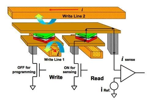
figure 2). This change in impedance represents the state of the data (“1” or “0”). Sensing
(Read Cycle) is accomplished by measuring the impedance of the MTJ (figure 3). Read cycles in
MRAM devices are non-destructive and relatively fast (35ns). Read operations are
accomplished with a very low voltage across the MTJ, supporting unlimited operation over the
part lifetime.
Magnetic Tunnel Junction
Figure 1: Magnetic Tunnel Junction (MTJ)
Copyright © 2013 Everspin Technologies, Inc. 1 Application Note 02130 3/2013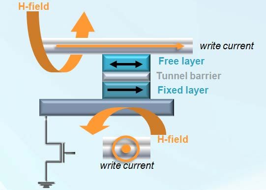
Comparing Technologies: MRAM vs. FRAM

              Figure 2: MRAM Magnetic Tunnel Junction (MTJ) Storage Element

                                Figure 3: MRAM Write/Read cycle

FRAM TECHNOLOGY
FRAM or Ferroelectric Random Access Memory uses a 1 transistor – 1 ferroelectric capacitor
(1T-1FC) architecture that employs ferroelectric materials as storage devices. These materials
have an intrinsic electric dipole switched into opposite polarities with an external electric field.
                                                                                             4+
Switching the ferroelectric polarization states requires the movement of the dipole (Ti           ion
Copyright © 2013 Everspin Technologies, Inc.       2               Application Note 02130 3/2013
Comparing Technologies: MRAM vs. FRAM
located within an oxygen octahedron (in the case of Pb(Zr,Ti)O3) in response to an electric field
(figure 4). This movement can be impeded by a free electric charge or other ionic defects built-
up over time and temperature. Such defects cause the dipoles to relax over time leading to
fatigue.
Figure 3: FRAM Atomic Structure Figure 4: FRAM Data States
A read operation in a FRAM is destructive because it requires switching the polarization state in
order to sense its state. The read operation has to restore the polarization to its original state
after the initial read which adds cycle time to the read operation.
Figure 5: FRAM Write/Read cycle
Copyright © 2013 Everspin Technologies, Inc. 3 Application Note 02130 3/2013Comparing Technologies: MRAM vs. FRAM
FRAM Read and Write cycles require an initial “Pre-charge” time which can increase the initial
access time.
FATIGUE
As mentioned earlier, MRAM technology uses magnetic states for data storage. Switching the
magnetic polarization between the two states does not require the motion of atoms and
therefore, there is no wear-out mechanism for a MRAM device. Bit storage in an FRAM
4+
requires the movement of its inherent electric dipole (Ti ion within the oxygen octahedron in
the case of Pb(Zr,Ti)O3) in response to an electric field. Over time, dipole movement will be
increasingly impeded by buildup of free electric charge in the capacitor and other ionic defects.
Furthermore, hydrogen bonding with the ferroelectric dipole is a known wear-out mechanism,
which is why H2 contamination is a concern in the CMOS BEOL manufacturing of FRAM.
IMPRINT/OPPOSITE STATE RETENTION
FRAM technology has an inherent asymmetry in the hysteresis behavior of the memory
elements. The bottom electrode has a higher thermal budget compared to the top electrode,
causing a preferred dipole orientation of the ferroelectric element. Over time, this preferred
orientation will eventually become so dominant that the external programming voltage will no
longer be able to reorient the dipole out of the preferred orientation. The memory cell
becomes locked into its preferred orientation causing a memory bit failure.
Another concern of FRAM technology is the reduction in polarization (signal) in response to
lower read voltages. Full supply voltage is applied to the capacitor during write operations
however, during read operations only part of the voltage is applied to the ferroelectric element
because the Read voltage is divided between parasitic capacitance and ferroelectric
capacitance. As a consequence, subsequent reads the voltage margin between states decreases
and can eventually lead to an inability to differentiate between states.
HIGH TEMPERATURE DATA RETENTION
Ambient operating temperatures above 85°C accelerate wear-out of FRAM due to build-up of
free electric charge resulting in imprint.
Everspin MRAM has been demonstrated in carefully designed experiments to retain data for up
to 20 years at 125°C.
Copyright © 2013 Everspin Technologies, Inc. 4 Application Note 02130 3/2013Comparing Technologies: MRAM vs. FRAM EXTENDED TEMPERATURE Extended temperature FRAM (Industrial and Automotive (AEC-Q100 Grade 1)) typically requires the use of a 2T-2FC architecture. This architecture allows for a self-reference read compensating for a weakening polarization (signal margin) at higher operating temperatures. Everspin MRAM requires no additional architecture changes to meet Industrial and Automotive temperature demands. MANUFACTURING Everspin MRAM products are fabricated using standard commercial CMOS fabrication technology. The magnetic elements are built between two Cu metal layers, typically the last and next-to-last metal layers. There is no deviation from standard BEOL CMOS processing except for the addition of magnetic cladding layers in the metal trenches. FRAM products are integrated on the W plug before the first BEOL metal layer. At the High temperatures of the FRAM process (650C required to deposit the PZT films) the W-plug is prone to oxidation making defect control a challenge. Before returning to standard BEOL CMOS processing, the ferroelectric capacitors must be encapsulated in AlOx to prevent diffusion of H2 into the other ferroelectric elements. SCALABILITY At fabrication nodes of 65nm or smaller, 3D architecture will be required to build the ferroelectric (FRAM) elements. As the feature size decreases, the risk of Imprint, or non- preferred orientation of ferroelectric dipoles increases. Everspin MRAM uses standard CMOS technology and has greater scalability with decreasing feature size without a significant cost premium. Copyright © 2013 Everspin Technologies, Inc. 5 Application Note 02130 3/2013
Comparing Technologies: MRAM vs. FRAM

Comparing FRAM and MRAM (MR0A08A vs. FM28V100, 2.7V to 3.6V)

          Attribute      FRAM                             MRAM

          Technology     1 transistor – 1 ferroelectric   1 transistor – 1 magnetic tunnel
                         capacitor (1T – 1FRC)            junction (1T – MTJ)
                 Read    Destructive                      Non-destructive
    Read Cycle Time      90ns                             35ns

   Read Access Time      60ns                             35 ns

    Write Cycle Time     90ns                             35ns

           Write (CE)    60ns                             35ns

                         Known wear-out mechanisms        No wear-out. Infinite Read /
              Fatigue
                         1014 Read / Write                Write

                         Increases with temperature
              Imprint    and decreasing operating         No Imprint
                         voltage
  High Temperature
                         Degrades above 85°C              20 years at 125°C (continuous)
     Data Retention

                         Complex – O2 ambient >650°C      Standard BEOL CMOS
      Manufacturing
                         process, H2 sensitivity.         processing
                         Need 3D structures at 65nm.
           Scalability   Imprint becomes more of an       Fully Scalable
                         issue.

                         Table 1: Attribute Comparison MRAM and FRAM

 Copyright © 2013 Everspin Technologies, Inc.        6            Application Note 02130 3/2013
Comparing Technologies: MRAM vs. FRAM
How to Reach Us:
Everspin Technologies, Inc.
Home Page:
www.everspin.com Information in this document is provided solely to enable system and software
implementers to use Everspin Technologies, Inc. products. There are no express or implied
E-Mail: licenses granted hereunder to design or fabricate any integrated circuit or circuits based
support@everspin.com on the information in this document. Everspin Technologies, Inc. reserves the right to
orders@everspin.com make changes without further notice to any products herein. Everspin makes no
sales@everspin.com warranty, representation or guarantee regarding the suitability of its products for any
particular purpose, nor does Everspin Technologies, Inc. assume any liability arising out of
USA/Canada/South and Central America the application or use of any product or circuit, and specifically disclaims any and all
Everspin Technologies, Inc. liability, including without limitation consequential or incidental damages. “Typical”
1347 N. Alma School Road, Suite 220 parameters, which may be provided in Everspin Technologies, Inc. data sheets and/or
Chandler, Arizona 85224 specifications can and do vary in different applications and actual performance may vary
+1-877-347-MRAM (6726) over time. All operating parameters including “Typical” must be validated for each
+1-480-347-1111 customer application by `-customer’s technical experts. Everspin Technologies, Inc. does
not convey any license under its patent rights nor the rights of others. Everspin
Technologies, Inc. products are not designed, intended, or authorized for use as
Europe, Middle East and Africa
components in systems intended for surgical implant into the body, or other applications
support.europe@everspin.com
intended to support or sustain life, or for any other application in which the failure of the
Everspin Technologies, Inc. product could create a situation where personal injury or
Japan
death may occur. Should Buyer purchase or use Everspin Technologies, Inc. products for
support.japan@everspin.com
any such unintended or unauthorized application, Buyer shall indemnify and hold
Everspin Technologies, Inc. and its officers, employees, subsidiaries, affiliates, and
Asia Pacific
distributors harmless against all claims, costs, damages, and expenses, and reasonable
support.asia@everspin.com
attorney fees arising out of, directly or indirectly, any claim of personal injury or death
associated with such unintended or unauthorized use, even if such claim alleges that
Everspin Technologies, Inc. was negligent regarding the design or manufacture of the
part. Everspin™ and the Everspin logo are trademarks of Everspin Technologies, Inc., Inc. All other product or service names are the property of their respective owners.
Copyright © 2013 Everspin Technologies, Inc.
Comparing FRAM and MRAM
Author: Chuck Bohac, Manager Applications Engineering, Everspin Technologies, Inc. chuck.bohac@everspin.com, 480-347-
1161
Copyright © 2013 Everspin Technologies, Inc. 7 Application Note 02130 3/2013You can also read