CU3TATE4: SYNTHESIS, X-RAY DIFFRACTION, SCANNING ELECTRON MICROSCOPY, AND DIFFUSE REFLECTANCE MEASUREMENTS
←
→
Page content transcription
If your browser does not render page correctly, please read the page content below
Grima et al, Vol. 7, Nro. 20, 9–15, enero–abril, 2021.
 Article:

 Cu3TaTe4: Synthesis, X-ray Diffraction, Scanning Electron Microscopy,
               and Diffuse Reflectance Measurements
            P. Grima-Gallardo1,2,3∗ , L. Nieves1,2,3         , A. Velasquez1,2       , G.E. Delgado4
                           1
                             Centro Nacional de Tecnologı́as Ópticas, Mérida, Venezuela
                           2
                            Centro de Investigaciones de Astronomı́a, Mérida, Venezuela
              3
                Centro de Estudios en Semiconductores, Departamento de Fı́sica, Facultad de Ciencias
                                   Universidad de Los Andes, Mérida, Venezuela
                  4
                    Laboratorio de Cristalografı́a, Departamento de Quı́mica, Facultad de Ciencias
                                   Universidad de Los Andes, Mérida, Venezuela

Recibido: marzo 2021
Aceptado: abril 2021
Autor para correspondencia: P. Grima-G. e–mail: peg1952@gmail.com
DOI: https://doi.org/10.5281/zenodo.4968549

                                                     Abstract
        In the present investigation Polycrystalline samples of Cu3 TaTe4 were prepared by the melt and anneal
     method. X-Ray Diffraction (XRD) and Diffuse Reflectance Spectroscopy (DRS) measurements were
     performed to verify the crystal structure and calculate the indirect and direct band gaps. The results
     showed a lattice parameter a = 5.9082 Å, a stoichiometry with a Ta deficit of 17.8 %, indirect bandgap
     Egi = 0.38 eV, and a direct gap Egd = 2.38 eV. The analyzes confirm that Cu3 TaTe4 can be used as an
     p-type absorbent for thin film solar cells with the advantages that its elements have low toxicity and have
     lower costs than those used today.
     Key words: Cu3 TaTe4 ; diffuse reflectance; optical bandgap.

 Artı́culo:

     Cu3TaTe4: Medidas de sı́ntesis, difracción de rayos X, microscopı́a
               electrónica de barrido y reflectancia difusa
                                                     Resumen
        En la presente investigación fueron preparadas muestras policristalinas de Cu3 TaTe4 por el método de
     fusión y recocido. Se realizaron medidas de difracción de rayos X (DRX) y espectroscopı́a de reflectancia
     difusa (ERD) para verificar la estructura cristalina y calcular las brechas de energı́a directa e indirecta.
     Los resultados mostraron un parámetro de red a = 5, 9082 Å, una estequiometrı́a deficitaria en Ta del
     17,8 %, una brecha de energı́a indirecta Egi = 0, 38 eV y una brecha de energı́a directa Egd = 2, 38 eV. Los
     análisis confirman que el Cu3 TaTe4 puede ser empleado como absorbente p-tipo para células solares de
     pelı́culas finas con las ventajas de que sus elementos presentan baja toxicidad y tienen costos menores a
     los empleados en la actualidad.
     Palabras claves: Cu3 TaTe4 ; reflectancia difusa; brecha óptica de energı́a.

Ciencia en Revolución, ISSN–e: 2610–8216,          CNTQ, Mincyt                          Ciencia y tecnologı́a 9
Grima et al, Vol. 7, Nro. 20, 9–15, enero–abril, 2021.

1    Introduction                                          et al. (5.906 Å) [2], (6.033 Å) [9]. No experimental
                                                           data for optical properties, as the bandgap (Eg ),
The sulvanite family of compounds, with chem-              were found in the literature.
ical formula Cu3 -TM-VI4 , (TM is the transi-                 In this work, the measurement of the bandgap
tion metal V, Nb, or Ta and VI is S, Se,                   value for Cu3 TaTe4 is reported for the first
or Te), is composed of nine members; three                 time. The bandgap is essential for applications in
sulfides: Cu3 VS4 , Cu3 NbS4 , Cu3 TaS4 ; three se-        optoelectronic devices as light detectors and solar
lenides: Cu3 VSe4 , Cu3 NbSe4 , Cu3 TaSe4 ; and three      cells.
tellurides: Cu3 VTe4 , Cu3 NbTe4 , Cu3 TaTe4 . They
are all semiconductors. As-growth samples show p-
type electrical conductivity, high ionic mobility, low     2     Experimental procedure
hole effective mass, high optical absorption in the
visible and UV range, and optical bandgaps suitable        2.1   Synthesis
for their use as an absorber layer in thin-film solar
                                                  Polycrystalline samples of Cu3 TaTe4 have been
photovoltaic devices [1, 2].
                                                  produced by the melt and anneal method as is
   Sulvanites crystallize in the cubic structure, space
                                                  described below. Starting materials (Cu, Ta, and
group (N 215), consisting of Cu, TM and VI atoms
                                                  Te) with nominal purity of 99.99 wt. % in the
located at the atom-sites (Wyckoff coordinates): 3d
                                                  stoichiometric ratio were mixed in an evacuated
(0.5, 0, 0), 1a (0, 0, 0) and 4e (u, u, u), respectively
                                                  (10−4 Torr) and sealed the quartz tube with the
(Figure 1) [3, 4, 5], described for the first time by
                                                  inner walls previously carbonized to prevent the
Pauling and Hultgren [6] for the natural mineral,
                                                  chemical reaction of the elements with quartz. The
Cu3 VS4 .
                                                  quartz ampoule is heated until 723 K (melting
                                                  point of Te) keeping this temperature for 48 h and
                                                  shaking all the time using an electromechanical
                                                  motor. This procedure guarantees the formation of
                                                  binary species at low temperatures avoiding the
                                                  existence of free Te at high temperatures, which
                                                  could produce Te deficiency in the ingot. Then the
                                                  temperature was slowly increased until 1423 K, with
                                                  the mechanical shaker always connected for better
                                                  mixing of the components. After 24 h, the cooling
                                                  cycle begins until the anneal temperature (800 K)
                                                  with the mechanical shaker is disconnected. The
Figure 1: The unit cell of sulvanite Cu3 TaTe4 . ampoule is keeping at the annealing temperature
Image created using Diamond software version 3.2e for 30 days to assure thermal equilibrium. Then the
with lattice parameter a = 6.025 Å [7] and anion furnace is switching off, letting naturally cooling the
displacement u = 0.2558 [7]                       ampoule to room temperature.

                                                           2.2   X-Ray Diffraction (XRD)
   Although this semiconductor family has been
extensively studied by ab initio calculations [2]-[5],     X-ray powder diffraction data were collected
[7]-[17] experimental results are relatively scarce, in    employing a diffractometer (Siemens D5005)
particular for Cu3 TaTe4 . The experimental value          equipped with a graphite monochromator (CuKα
of the lattice parameter a for Cu3 TaTe4 has been          λ = 1.54059 Å) at 40 kV and 20 mA. Silicon powder
reported by Hulliger [18], Zitter et al. [19], and Li      was used as an external standard. The samples were
et al. [20] as 5.928 Å, 5.9283 Å, and 5.930(2) Å,       scanned from 10 − 100◦ 2θ, with a step size of 0.02◦
respectively; in good agreement with theoretical           and counting time of 20 s. The Bruker analytical
calculations of Hong et al. (6.01 Å) [13] and Kehoe       software was used to establish the positions of

Ciencia en Revolución, ISSN–e: 2610–8216,        CNTQ, Mincyt                        Ciencia y tecnologı́a 10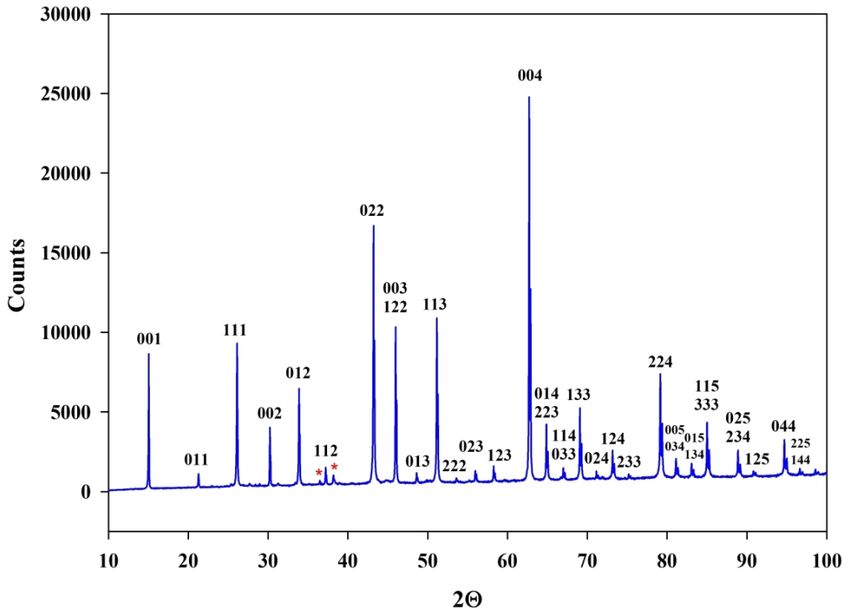
Grima et al, Vol. 7, Nro. 20, 9–15, enero–abril, 2021.

Figure 2: X-ray diffraction pattern of Cu3 TaTe4 . The numbers over the peaks correspond to the hkl-Miller
indices. Red asterisks signal two unidentified peaks

the peaks from the CuKα1 component and to             2.4   Diffuse     Reflectance        Spectroscopy
strip mathematically the CuKα2 components from              (DRS)
each reflection. The peak positions were extracted
employing a single-peak profile fitting carried out Optical absorbance has been measured in the
through the Bruker DIFFRACplus software. Each       energy range 0.5 to 6 eV using Diffuse Reflectance
reflection was modeled utilizing a pseudo-Voigt     Spectroscopy (DRS) technique using a UV-Visible-
function.                                           IR spectrophotometer equipped with a diffuse
                                                    reflectance accessory (integrating sphere) capable
                                                    of collecting the reflected flux. The sample was
2.3 Scanning           Electron       Microscopy ground in an agate mortar to obtain a fine powder
       (SEM)                                        (< 10 µm). Barium sulfate (Merck DIN 5033) was
                                                    used as an internal standard.
Stoichiometric relations were investigated by scan-
ning electron microscopy (SEM) technique, using
Hitachi S2500 equipment. The microchemical com- 3 Results and discussion
position was found by an energy-dispersive x-ray
spectrometer (EDS) coupled with a computer-based 3.1 X-ray diffraction
multichannel analyzer (MCA, Delta III analysis,
and Quantex software, Kevex). For the EDS anal- Figure 2 shown the X-ray diffraction pattern. Using
ysis, Kα lines were used. The accelerating voltage DIVOL06 software [21] the lattice parameter has
was 15 kV. The samples were tilted 35 degrees. A been calculated as a = 5.9082 Å in good agreement
standardless EDS analysis was made with a relative with previous reports [22]. Traces of a secondary
error of ±(5 − 10) % and detection limits of the phase, signaled by red asterisks in Figure 2, are also
order of 0.3 wt %, where the k-ratios are based on observed; however, this phase cannot be unambigu-
theoretical standards.                              ously identified with the present information.

Ciencia en Revolución, ISSN–e: 2610–8216,     CNTQ, Mincyt                       Ciencia y tecnologı́a 11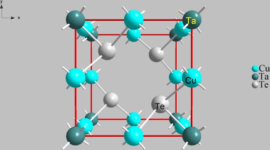
Grima et al, Vol. 7, Nro. 20, 9–15, enero–abril, 2021.

                  Table 1: Scanning Electron Microscopy (SEM) results for Cu3 TaTe4
                                 Weight Concentration %                       Atom Concentration %
                            Cu              Ta            Te             Cu           Ta             Te
       Cu3 TaTe4 pt1   23.35 ± 0.52 10.06 ± 0.25 66.59 ± 0.70       36.83 ± 0.83 10.85 ± 0.26 52.32 ± 0.55
       Cu3 TaTe4 pt2   23.19 ± 0.54    9.90 ± 0.25   66.91 ± 0.72   36.65 ± 0.85 10.70 ± 0.27 52.65 ± 0.57
       Cu3 TaTe4 pt3   24.31 ± 0.56    8.94 ± 0.23   66.76 ± 0.72   38.18 ± 0.88  9.60 ± 0.25   52.22 ± 0.57
       Cu3 TaTe4 pt4   23.48 ± 0.56    9.69 ± 0.17   66.83 ± 0.73   37.04 ± 0.88 10.45 ± 0.18 52.51 ± 0.58
       Cu3 TaTe4 pt5   23.05 ± 0.56    8.98 ± 0.16   67.97± 0.74    36.56 ± 0.88  9.75 ± 0.18   53.69 ± 0.58
       Mean values         23.48           9.51          67.01          37.05        10.27          52.68

3.2   Scanning         Electron          Microscopy K and S are the absorption and scattering
      (SEM)                                        coefficients of the sample, respectively; R∞ is
                                                   the reflectance, and F (R∞ ) is usually termed
To verify the stoichiometry SEM measurements
                                                   the remission or Kubelka-Munk (K-M) function.
were performed. Figure 3 display the corresponding
                                                   Figure 4 show the (K-M) function for Cu3 TaTe4 .
microphotography, indicating the five (5) points
where the experimental stoichiometry was mea-
sured. Table 1 present the obtained values. The
calculated nominal stoichiometry of Cu3 TaTe4 , in
atom concentration, is Cu = 37.5 %, Ta = 12.5 %,
and Te = 50.0 %; the porcentual deviations with
respect to the mean experimental values are
Cu = 1.2 %, Ta = 17.8 % and Te = 5.4 %.

                                                           Figure 4: Experimental absorbance for Cu3 TaTe4 .
                                                           The numbers correspond to the energies of the
                                                           absorption bands
Figure 3: Microphotography of Cu3 TaTe4 . The
numbers signal the points where the stoichiometry
was measured in correspondence with Table 1                   The experimental absorbance of Cu3 TaTe4 in
                                                           the energy interval 1 < E(eV ) < 6 shows several
                                                           structures or energy bands that, in the absence of
3.3   Diffuse reflectance                                  other experimental results, can be compared with
                                                           calculations of Kehoe et al. [2], Ali et al. [7] and
The optical absorption of Cu3 TaTe4 was measured
                                                           Espinoza et al. [8]. It is founding a relatively good
at ambient conditions using the diffuse reflectance
                                                           agreement because the off-stoichiometric character
technique [23] where the reflectance F (R∞ ) is given
                                                           of real samples is not properly represented in
by the Equation (1)
                                                           theoretical studies. It was postulated that intrinsic
            K   (1 − R∞ )2                                 defects within the material affect the bandgap
              =            = F (R∞ ) ,               (1)   as measured by optical spectroscopy, something
            S      2R∞

Ciencia en Revolución, ISSN–e: 2610–8216,         CNTQ, Mincyt                         Ciencia y tecnologı́a 12
Grima et al, Vol. 7, Nro. 20, 9–15, enero–abril, 2021.
that can be accounted for if excitonic effects were gen atom (S, Se, Te); and effectively, comparing
considered [1]. the direct bandgap of Cu3 TaTe4 (2.39 eV) (this
Concerning the energy gap, it is accepted work), Cu3 TaSe4 (2.43 eV) [22], and Cu3 TaSe4
that fundamental band gaps of all sulvanites (2.76 eV) [25], value of the present work accom-
are naturally indirect [9] because the conduction plished the empirical rule.
band minimum (CBM ) is located at X point of
the Brillouin Zone (BZ ) while the valence band Table 2: Comparative bandgaps values for
maximum (VBM ) is located at R point of the Cu3 TaTe4
BZ [7]. In consequence, indirect transitions are Egi [eV] Egd [eV] Reference
R → X type, whereas direct transitions (if they are 1.11 1.69 Kahoe et al. [2]
not forbidden) are at X point. 1.112, 1.837, 0.972 Ali et al. [7]
1.171, 1.323 Hong et al. [13]
0.38 2.39 This work
In Table 2, the experimental values are compared
with previous calculations.
4 Conclusion
Cu3 TaTe4 has been synthesized by the melt-anneal
method and characterized by DRX, SEM, and
Diffuse Absorption. DRX and SEM show a poly-
crystalline sample with a = 5.9082 Å in agreement
with previous reports and a stoichiometric deficit
Figure 5: Absorbance (left), indirect (center), and of Ta (17.8 %). The indirect and direct bandgaps
direct (right) optical energy gaps of Cu3 TaTe4 were measured as Egi = 0.38 eV and Egi = 2.39 eV,
respectively. These results confirm that Cu3 TaTe4
may be a good candidate as p-type absorber
In Figure 5, using the absorption of Figure 4 and material for thin-film solar cells with the advantages
Tauc’s plot method [24], direct (X) and indirect that their elements are not so toxic as Cd, less
(R → X) transitions values have been obtained expensive than Ga, and more abundant than the
founding Egi = 0.38 eV and Egd = 2.39 eV. The Egi rare In, materials that are extensively used in
results too much lower than those calculated theo- the actuality. Also, it can be used with window
retically. Usually, theoretical calculations produce materials, as CdS with a lattice mismatch of only
values that are lower than experimental [7] in 1.53 %.
consequence the disagreement must become from
the polycrystalline character of the sample. The
fingerprint of cationic disorder is the broad shoulder
References
in the direct gap curve of Figure 5. Defect states and [1] R. Prado-Rivera, C.-Y. Chang, M. Liu, C.-Y.
phonon absorption produce an additional optical Lai, and D.R. Radu. Sulvanites: The Promise
absorption at energies a little lower than the at the Nanoscale. Nanomaterials, 11:823, 2021.
bandgap. https://doi.org/10.3390/nano11030823.
The direct gap Egd value is higher than those
calculated as usually happens. However, the curve of [2] A. B. Kehoe, D. O. Scanlon, and G. W.
Egd fits very well with Tauc’s method clearly showing Watson. The Electronic Structure of Sulvanite
an absorption front. The bandgap of sulvanites Structured Semiconductors Cu3 MCh4 (M =
increases with the atomic number of the chalco- V, Nb, Ta; Ch = S, Se, Te): Prospects
Ciencia en Revolución, ISSN–e: 2610–8216, CNTQ, Mincyt Ciencia y tecnologı́a 13Grima et al, Vol. 7, Nro. 20, 9–15, enero–abril, 2021.
for Optoelectronic Applications. Journal of Absorbers Cu3 MCh4 (M = V, Nb, Ta; Ch =
Materials Chemistry C3, C3(12236), 2015. S, Se, Te) Using Density Functional. Jour-
https://doi.org/10.1039/c5tc02760h. nal Physics: Condensed Matter, 28:175801,
2016. https://doi.org/10.1088/0953-8984/28
[3] M. A. Ali, N. Jahan, and A. K. M. A. Islam. /17/175801.
Sulvanite Compounds Cu3 TMS4 (TM = V, Nb,
and Ta): Elastic, Electronic, Optical, and Ther- [10] X.-P. Liu, Z.-Z. Feng, S.-P. Guo, Y. Xia, and
mal Properties using First-principles Method. Y. Zhang. Promising Thermoelectric Materials
Journal Science Research, 6(3):407–419, 2014. of Cu3 VX4 (X = S, Se, Te): A Cu-V-X Frame-
http://dx.doi.org/10.3329/jsr.v6i3.19191. work Plus Void Tunnels. International Journal
of Modern Physics C, 30(8):1950045, 2019.
[4] W.F. Espinosa-Garcı́a, C.M.Ruiz-Tobón, and https://doi.org/10.1142/S0129183119500451.
J.M.Osorio-Guillén. The Elastic and
Bonding Properties of the Sulvanite Com- [11] J. Peralta and C. Valencia-B. Vibrational
pounds: A Girst-principles Study by Local Properties of Cu3 XY4 Sulvanites (X
and Semi-local Functionals. Physica B: = Nb, Ta, and V; and Y = S, and
Condensed Matter, 406(20):3788–3793, 2011. Se) by Ab initio Molecular Dynamics.
https://doi.org/10.1016/j.physb.2011.06.060. European Physic Journal B, 90(117), 2017.
https://doi.org/10.1140/epjb/e2017-80050-7.
[5] J.M. Osorio-G. and W.F. Espinosa-G. A
First-principles Study of the Electronic Struc- [12] K. Bougherara, F. Litimein, R. Khenata,
ture of the Sulvanite Compounds. Physica E. Uçgun, H.Y. Ocak, S. Uğur, G. Uğur,
B: Condensed Matter, 407(6):985–991, 2012. A.H. Reshak, F. Soyalp, and S.B Om-
https://doi.org/10.1016/j.physb.2011.12.126. ran. Structural, Elastic, Electronic, and
Optical Properties of Cu3 TMSe4 (TM = V,
[6] P. Linus and H. Ralph. The Crystal Structure Nb, and Ta) Sulvanite Compounds via
of Sulvanite, Cu3 VS4 . Zeitschrift für Kristallo- First-Principles Calculations. Science
graphie – Crystalline Materials, 84(1–6):204– of Advanced Materials, 5(1):97–106, 2019.
212, 1993. https://doi.org/10.1524/zkri. https://doi.org/10.1166/sam.2013.1435.
1933.84.1.204.
[13] A.J. Hong and C.L. Yuan and G. Gu and J.
[7] M.A. Ali, M. Roknuzzaman, M.T. Nasir, M. Liu. Novel p-type Thermoelectric Ma-
A.K.M.A. Islam, and S.H. Naqib. Struc- terials Cu3 MCh4 (M = V, Nb, Ta; Ch =
tural, Elastic, Electronic, and Optical Prop- Se, Te): High Band-degeneracy. Journal
erties of Cu3 MTe4 (M= Nb, Ta) Sulvan- Materials Chemistry A, 5:9785–9792, 2017.
ites, an Ab Initio Study. International https://doi.org/10.1039/C7TA02178J.
Journal Modern Physics B, 1650089, 2016.
https://doi.org/10.1142/S0217979216500892. [14] J. Li, H.-Y. Guo, D.M. Proserpio, and
A. Sironi. Exploring Tellurides: Synthesis
[8] W.F. Espinosa-G. and S. Pérez-W. and J.M. and Characterization of New Binary, Ternary,
Osorio-G. and C Moyses A. The and Quaternary Compounds. Journal of
Electronic and Optical Properties of Solid State Chemistry, 117(2):247–255, 1995.
the Sulvanite Compounds: A Many- https://doi.org/10.1006/jssc.1995.1270.
body Perturbation and Time-dependent
Density Functional Theory Study. Journal [15] Y. Liu, M. Liu, and M.T. Swihart. Plasmonic
Physics: Condensed Matter, 30:035502, 2018. Copper Sulfide-Based Materials: A Brief
https://doi.org/10.1088/1361-648X/aa9deb. Introduction to Their Synthesis, Doping,
Alloying, and Applications. Journal Physics
[9] A.B. Kehoe and D.O. Scanlon and G.W. Chemistry C, 121(25):13435–13447, 2017.
Watson. Modelling Potential Photovoltaic https://doi.org/10.1021/acs.jpcc.7b00894.
Ciencia en Revolución, ISSN–e: 2610–8216, CNTQ, Mincyt Ciencia y tecnologı́a 14Grima et al, Vol. 7, Nro. 20, 9–15, enero–abril, 2021.
[16] Y. Li, M. Wu, T. Zhang, X. Qi, G. Ming, Society of America, 38(5):448–457, 1948.
G. Wang, X. Quan, and D. Yang. Natu- https://doi.org/10.1364/JOSA.38.000448.
ral Sulvanite Cu3 MX4 (M = Nb, Ta; X = S,
Se): Promising Visible-light Photocatalysts for [24] J. Tauc. Optical Properties and Electronic
Water Splitting. Computational Materials Structure of Amorphous Ge and Si.
Science, 165:137–143, 2019. https://doi.org/ Materials Research Bulletin, 3:37, 1968.
10.1016/j.commatsci.2019.04.042. https://doi.org/10.1016/0025-5408(68)90023-
8.
[17] W.F. Espinosa-G., C. Valencia-B., and J.M.
Osorio-G. Phononic and thermodynamic [25] P.F. Newhouse, P.A. Hersh, A. Zakutayev,
properties of the sulvanite compounds: A first- A. Richard, H.A.S. Platt, D.A. Keszler,
principles study. Computational Materials and J. Tate. Thin-film Preparation and
Science, 113:275–279, 2016. https://doi.org/ Characterization of Wide Bandgap Cu3 TaQ4
10.1016/j.commatsci.2015.10.036. (Q = S or Se) p-type Semiconductors.
Thin Solid Films, 517:2473–2476, 2009.
[18] F. Hulliger. New semiconductor compounds https://doi.org/10.1016/j.tsf.2008.11.020.
of the sulvanite type. Helvetica Physics Acta,
34:379–382, 1961.
[19] K. Zitter, J. Schmand, K. Wagner, and
R. Schöllhorn. Isomer shifts of the 6.2 keV
nuclear transition of Ta-181 in sulvanite
type ternary phases Cu3 TaX4 (X = S, Se,
Te). Material Research Bulletin, 19:801–
805, 1984. https://doi.org/10.1016/0025-
5408(84)90038-2.
[20] J. Li, H.-Y. Guo, D.M. Proserpio, and
A. Sironi. Exploring Tellurides: Synthe-
sis and Characterization of New Binary,
Ternary, and Quaternary Compounds. Jour-
nal Solid State Chemistry, 117:247–255, 1995.
https://doi.org/10.1006/jssc.1995.1270.
[21] A Boultif and D. Louer. Powder Pattern
Indexing with the Dichotomy Method. Journal
of Applied Crystallography, 37:724–731, 2004.
https://doi.org/10.1107/S0021889804014876.
[22] P. Grima-G., M. Salas, O. Contreras, Ch.
Power, M. Quintero, H. Cabrera, I. Zumeta-D.,
A. Rodrı́guez, J.A. Aitken, and W. Brämer-
E. Cu3 TaSe4 and Cu3 NbSe4 : X-ray Diffrac-
tion, Differential Thermal Analysis, Optical
Absorption, and Raman Scattering. Journal
of Alloys and Compounds, 658:749–756, 2016.
https://doi.org/10.1016/j.jallcom.2015.10.283.
[23] P. Kubelka. New Contributions to the
Optics of Intensely Light-Scattering Mate-
rials. Part I. Journal of the Optical
Ciencia en Revolución, ISSN–e: 2610–8216, CNTQ, Mincyt Ciencia y tecnologı́a 15You can also read