Deep Neural Network Acceleration in Non-Volatile Memory: A Digital Approach

Page created by Rose Romero
 
CONTINUE READING
Deep Neural Network Acceleration in Non-Volatile Memory: A Digital Approach
Deep Neural Network Acceleration in Non-Volatile
          Memory: A Digital Approach
                                               Shaahin Angizi and Deliang Fan
           Department of Electrical and Computer Engineering, University of Central Florida, Orlando, FL 32816
                                       Email: angizi@knights.ucf.edu, dfan@ucf.edu

   Abstract—Latest algorithmic development has brought com-         utilizing the inherent memory parallelism and huge internal
petitive classification accuracy for neural networks despite        memory bandwidth. Such mechanism is expected to bring
constraining the network parameters to ternary or binary
representations. These findings show significant optimization
                                                                    significant efficiency in the off-chip data transfer latency
opportunities to replace computationally-intensive convolution      and energy. Meanwhile, a lot of research efforts have been
operations (based on multiplication) with more efficient and less   carried out in emerging technology based on Non-Volatile
complex operations such as addition. In hardware implemen-          Memory (NVM), such as resistive RAM (ReRAM) [4], Mag-
tation domain, processing-in-memory architecture is becoming        netic RAM (MRAM) and etc. Spin-Transfer Torque Magnetic
a promising solution to alleviate enormous energy-hungry data
communication between memory and processing units, bringing
                                                                    Random Access Memory (STT-MRAM) [14] and Spin-Orbit
considerable improvement for system performance and energy          Torque Magnetic Random Access Memory (SOT-MRAM) [5]
efficiency while running such large networks. In this paper,        are energy-efficient and high performance candidates, mainly
we review several of our recent works regarding Processing-in-      owning to superior endurance, low switching energy, CMOS
Memory (PIM) accelerator based on Magnetic Random Access            technology compatibility, etc. By leveraging such intrinsic
Memory computational sub-arrays to accelerate the inference
mode of quantized neural networks using digital non-volatile
                                                                    resistive property, the bulk bit-wise in-memory operations such
memory rather than using analog crossbar operation. In this         as AND/OR/XOR have been implemented through the method
way, we investigate the performance of two distinct in-memory       of routed sensing [15]–[17], that opens a novel route to realize
addition schemes compared to other digital methods based on         efficient PIM platforms. Although, this effort has been limited
processing-in-DRAM/GPU/ASIC design to tackle DNN power              to fundamental logic operations so far. Such functions are
and memory wall bottleneck.
                                                                    not necessarily applicable to many tasks except by imposing
   Index Terms—Depp Neural network acceleration, In-memory
computing, Magnetic Random Access Memory                            multi-cycle operations [16], [18] to implement more complex
                                                                    combinational logics such as addition.
                      I. I NTRODUCTION                                 In this paper, we review several of our recent works about
                                                                    acceleration of in-memory addition operations that could be
   To reduce the massive MAC operations and memory re-              used in Binary-Weight DNNs (BWNNs) in an SOT-MRAM
quirement in Deep Convolutional Neural Networks (DNN), re-          based in-memory computing platform, based on set of mi-
searchers have proposed various quantized/binarized DNNs by         croarchitectural and circuit-level designs.
limiting inputs, weights or gradients to be quantized/ binarized
specifically in forward propagation [1], [2].The DoReFa-Net                  II. B INARY-W EIGHT N EURAL N ETWORKS
achieves high accuracy over both SVHN and ImageNet data-               DNN performs in two distinct modes, in training mode, the
sets with various low bit-width configurations after applying       configuration parameters of layers are computed by training
quantization methods [1]. Besides, the extremely-quantized          the network on pre-classified images, and in inference mode,
Binary Neural Networks (BNNs) have obtained close accuracy          test images are fed to the network for examination. As
to existing DNNs [2]. An identical yet updated version of bi-       mentioned earlier, Multiplication and Accumulation operations
nary training has been also applied for Generative Adversarial      (MAC) accounts for the most arithmetic operations [19] used
Networks (GANs) [3] to reduce the memory utilization, thus          in both modes. To remove the need for massive multiplication
improving the hardware deployment efficiency.                       operations and memory storage, researchers have developed
   From DNN/GAN accelerator architecture perspective, the           various Binary-Weight DNNs (BWNN) by constraining the
isolated processing and memory units (i.e., GPU or CPU)             weights to binary values in forward propagation. BinaryCon-
are connected through buses which has dealt with a wide             nect [2] achieves close results to full-precision networks on
variety of challenges, i.e. congestion at I/Os, long memory         MNIST and CIFAR-10 data-sets by training the networks with
access latency, limited memory bandwidth, huge data transfer        binary weights (-1, +1). This method can potentially replace
energy and leakage power for saving network parameters in the       computationally-intensive multiplication operations with much
volatile memory [4]. To alleviate such concerns, Processing-in-     simpler complement addition/subtraction operations [19]. Such
Memory (PIM) platforms has been widely explored in recent           replacement remarkably reduces weight storage requirements.
accelerators design [4]–[13] to bring a potential solution for      The following equation [2] gives the binarization functions
memory wall challenge. The major idea of PIM is to realize          in deterministic and stochastic way for wf p (floating point
computational logic units inside the memory to process data         weights):
Deep Neural Network Acceleration in Non-Volatile Memory: A Digital Approach
resistance in both magnetic layers is represented by ‘0’ and is
                                                       
                                                                     +1, wf p ≥ 0
                                                                                                                                   
                                                                                                                                    +1,           p = σ(wf p )                              lower than that of anti-parallel magnetization resistance (‘1’).
                             wb,De =                                              , wb,St                                        =                                                   (1)
                                                                     −1, wf p < 0                                                    −1,          1−p                                       Every SOT-MRAM bit-cell in computational sub-arrays is
  where σ denotes a hard sigmoid function that determines                                                                                                                                   connected to five controlling signals namely Write Word Line
the distribution probability:                                                                                                                                                               (WWL), Write Bit Line (WBL), Read Word Line (RWL), Read
                                                                                                                                                                                            Bit Line (RBL), and Source Line (SL). The computational sub-
                                                                            x+1                         x+1                                                                                 array is mainly developed to realize the computation between
                                   σ(x) = clip(                                 , 0, 1) = max(0, min(1,     ))                                                                       (2)
                                                                             2                           2                                                                                  in-memory operands using two different mechanisms as called
   Now, we present the MRAM platform to accelerate BWNNs                                                                                                                                    two-row activation and three-column activation. These mech-
in the PIM context.                                                                                                                                                                         anisms will be later used to respectively implement bulk bit-
                                                                                                                                                                                            wise in-memory AND and addition/subtraction (add/sub).
                              III. P ROCESSING - IN -MRAM ACCELERATOR                                                                                                                             a) Bit-line Computation Mode: The presented SOT-
   The presented accelerator architecture is depicted in Fig. 1a                                                                                                                            MRAM sub-array is developed to realize the bulk bit-wise in-
with computational SOT-MRAM sub-arrays, kernel and image                                                                                                                                    memory logic operations between every two or three operands
banks, and a Digital Processing Unit (DPU) with three sub-                                                                                                                                  positioned in the similar bit-line. Generally, in the 2-/ 3-
components as represented by Binarizer, Activation Function,                                                                                                                                input in-memory logic method, every two/three bits stored
and Batch Normalization. The platform is mainly controlled                                                                                                                                  in the identical column are selected with the MRD [20] and
by Ctrl (located in each sub-array) to run whole BWNNs.                                                                                                                                     simultaneously sensed by SA connected to the same bit-
In the first step, with Kernels (W ) and Input feature maps                                                                                                                                 line. Accordingly, a programmable SA’s reference selected
(I) that are respectively saved in Kernel and Image Banks,                                                                                                                                  by Ctrl will be compared with the equivalent resistance of
W has to be instantly binarized for mapping into sub-arrays.                                                                                                                                such parallel connected bit cells and their cascaded access
Note that this doesn’t apply to the first layer [1]. Moreover,                                                                                                                              transistors after injecting a small amount of current over
binarized shared kernels will be used for different inputs.                                                                                                                                 resistors. Through selecting different reference resistances e.g.
This operation is implemented through DPU’s Binarizer-Bin.                                                                                                                                  RAN D2 and ROR2 , the SA can perform basic 2-input in-
(shown in Fig. 1a) and then outputs are sent to the sub-arrays,                                                                                                                             memory Boolean functions AND and OR, respectively. For
developed to handle the computational load employing PIM                                                                                                                                    example, to realize AND operation, Rref is set at the midpoint
methods. In the second and third steps, as will be throughly                                                                                                                                of RAP //RP (‘1’,‘0’) and RAP //RAP (‘1’,‘1’). With the
explained in the next subsections, the parallel computational                                                                                                                               data organization shown in Fig. 1b, where A and B operands
sub-arrays perform to feature extraction employing combining                                                                                                                                correspond to M1 and M2 memory cells, respectively, 2-
and parallel compute. schemes. Eventually, the accelerator’s                                                                                                                                input in-memory method outputs AB in only one memory
DPU activates the resultant feature map to complete the fourth                                                                                                                              cycle. The idea of voltage comparison between Vsense and
step by producing output feature map.                                                                                                                                                       Vref is shown on Fig. 2 for different operations. The reconfig-
                                                                                                                                            MCD                                             urable SA can also provide 2-input NOR, NAND functions
                                                                                                                                 Ctrl

                                                      Image Bank                                                                            WD                                 MCD
                                     I1[31]
                                     I2[31]
                                                I1[30]
                                                I2[30]
                                                             I1[29]
                                                             I2[29]
                                                                           I1[[2]
                                                                               2]
                                                                           I2[2]
                                                                                    I1[[1]
                                                                                        1]
                                                                                    I2[1]
                                                                                             I1[[0]
                                                                                                 0]
                                                                                             I2[0]
                                                                                                                    Conv (I,W)          A                  V1
                                                                                                                                                                 WWL1
                                                                                                                                                                                       SA   through the complementary outputs. Here, we present two
                                                                                                                                        B                        M1
                                                                                                                                                                                            reconfigurable SAs [8], [21], as shown in Fig. 3, that can
                                                                                                                                                          WBL1

                                                                                                                                                                        RBL1
                                                                                                                                 MRD

                                                                                                                 Output fmaps
                                                                                                                                                    MRD

                                                      Kernel Bank                                                                                                                    RWL1
                                                                                                                                                                                     SL1
                                                                                                                                                                  M2
                                     W1[31] W1[30] W1[29]
                                     W2[31] W2[30] W2[29]
                                                                           W1[[2]
                                                                               2] W1[[1]
                                                                                      1] W1[[0]
                                                                           W2[2] W2[1] W2[0]
                                                                                             0]

                                                                                                                 DPU                                                                 RWL2
                                                                                                                                                                                     SL2
                                                                                                                                                                                            be used alternatively through a direct connection to the same
                                                                                                                      Active.
                                      (1) Mapping Binary weights                                             Bin.                 SA                                                        computational sub-array BL to perform the computation.
  Accelerator Units

                      Compute.                                                                                        BN
                      Sub-arrays                                                                                                            MCD
                                                                                                                                 Ctrl

                                                                                                                                                                               MCD
                                        Ctrl          Ctrl                                    Ctrl
                                                                                                                                            WD
                                                                                                                                                                                                                                                      Iref

                                                                                                                                                                                                                                                                                                      Iref
                                                                                                                                                                                                                                        Isense

                                                                                                                                                                                                                                                                                         Isense
                                                                                                                                                                                                 Isense

                                                                                                                                                                                                               Iref

                                                                     (2) Combining                                                                                                     SA
                                                                                                                                                           V1
                                                         512 × 256
                                          512 × 256

                                                                                                 512 × 256

                                                                                                                                                                 WWL1
                                                                                                             (4) Activate.              A
                        Bin.                                                                                                                                     M1
                                                                                                                                                          WBL1

                                                                                                                                                                        RBL1

                      Activate.                                                                                                         B                                                                              Vsense                                   Vsense                                       Vsense
                                                                                                                                 MRD

                                                                                                                                                                                     RWL1
                                                                     (3) Parallel                                                                                                    SL1
                                                                                                                                                                 M2                                                                                                      SA                                           SA
                                                                                                                                                                                                                                     R1 RM1

                                                                                                                                                                                                                                                                                R1 RM1
                                                                                                                                                                                                                                                 R2 RM2

                        BN
                                                                                                                                                                                                                                                                                         R2 RM2
                                                                                                                                                    MRD

                                                                                                                                        C                                                                                       SA
                                                                                                                                                                                                   RM1

                                                                                                                                                                                                                                                                                                  R3 RM3

                                        #1 #2 compute.                                        #N                                                                                                                                                             Vref                                            Vref
                       DPU                                                                                              bias
                                                                                                                                                                                     RWL2
                                                                                                                                                                                     SL2                                Vref
                                                                                                                                                                                                                                                                RAND2

                                                                                                                                                                  M3
                                                                                                                                                                                                                                                                                                             RMAJ
                                                                                                                                                                                                                                                                         ROR2

                                         Compute. Sub-array
                                                                                                                                                                                                                                                                        or
                                                                                                                                                                                                                      RM
                                                                                                                                                                                                   R1

                                                                                                                                                                                     RWL3
                                                                                                                                  SA                                                 SL3

                                                                                                                                                                                                               Read                           OR AND                                                  MAJ
Fig. 1. (a) MRAM accelerator platform, (b) Computational sub-array design.                                                                                                                                              VAP          VP,P VAP,P VAP,AP
                                                                                                                                                                                                          VP                                                                     VP,P,P VP,P,AP VP,AP,APVAP,AP,AP
                                                                                                                                                                                                                      (a)                                 (b)                                       (c)
A. Sub-array with Reconfigurable Sense Amplifier                                                                                                                                            Fig. 2. Voltage comparison between Vsense and Vref for (a) read, (b) 2-input,
                                                                                                                                                                                            (c) 3-input in-memory logic operation.
   Fig. 1b illustrates the in-memory computing sub-array ar-
chitecture implemented by SOT-MRAM. This sub-array is                                                                                                                                            b) SA-I: The SA-I, as shown in Fig. 3a, has 2 sub-SAs
basically composed of a Memory Row Decoder (MRD), a                                                                                                                                         and 4 reference-resistance branches that could be enabled by
Memory Column Decoder (MCD), a Write Driver (WD)                                                                                                                                            Enable bits (ENM , ENOR2 , ENM AJ , ENAN D2 ) by the Ctrl
and n Sense Amplifier (SA) (n ∈ # of columns) that are                                                                                                                                      to implement both memory and computation operations based
adjustable by Ctrl to implement a dual mode computation                                                                                                                                     on Table I. The memory and single-threshold logic functions
i.e. memory write/read and in-memory logic operations. SOT-                                                                                                                                 could be readily realized only by activating one enable bit
MRAM device is a composite device of a spin Hall metal                                                                                                                                      at a time. As an instance, by enabling ENAN D2 , 2-input
(SHM) and a Magnetic Tunnel Junction (MTJ). Considering                                                                                                                                     AND/NAND function is carried out on the bit-line between
MTJ as the main storage element, the parallel magnetization                                                                                                                                 two operands. Besides, two enables can be activated at a
SA-II                       activating one enable in either branches at a time. Additionally,

                                                         ENNOR3

                                                                                               ENAND2
                                                                   ENOR2

                                                                                      ENAND3
                                                                                                        by activating more than two enables at a time, more thatn on

                                                                             ENMAJ
                                                   ENM
                               SA-I                                                                     logic functions could be simultaneously realized with SAs that
                  Isense
               Iref                                                                                     could be employed to generate complex multi-threshold logic
    RAND2

                Vref1                                                                                   functions such as XOR3/XNOR3.
                                                                  Vsense
                                                                                                           The computational sub-array can also perform add/sub
                      Vsense

               Iref                                      RBL

                                                                                                        operation based on SA-II but in a single cycle. With an
    RMAJ

                Vref2
                                                                                                        observation on the FA truth table, it can be observed that for
    ROR2

                                                                                      Carry
                                             Rst                                                        6 out of 8 possible input combinations, Sum output equals
                                                                     T1                        T2       inverted Carry signal. Besides, as discussed in SA-I, FA’s
    RM

            (ENM , ENOR2, ENMAJ, ENAND2)                                                                Carry is directly generated by MAJ function. Based on this,
                                                                                     Sum
                                                                                                        SA-II can realize such Sum and Carry outputs readily by MIN
                                                   (ENM , ENOR3 , ENOR2 , ENMAJ , ENAND3 , ENAND2)      and MAJ functions, respectively. Fig. 3b shows that the Sum bit
                                                                                                        is achieved from the SA’s MIN output. But, in order to consider
            Fig. 3. Sense amplifier designs: (a) SA-I [8], (b) SA-II [21]                               two extreme cases namely (0,0,0) and (1,1,1), we need to
                                                                                                        disconnect the MIN signal from Sum or else wrong result is
time e.g. ENOR2 , ENAN D2 , to generate two separate logic                                              achieved. It turns out that for these two cases, Sum signal can
functions, which is in particular useful to output double-                                              be implemented respectively by NOR3 (when T1:ON, T2:OFF
threshold logic functions like XOR/XNOR. Additionally, 3-                                               → Sum=0) and NAND3 functions (when T1:OFF, T2:ON →
input majority/minority functions (MAJ/MIN) in a single SA’s                                            Sum=1). This is implemented by inserting four additional pass
sensing cycle can be realized by selecting every three cells                                            transistors (two in the MIN function path for disconnecting
located in a same bit-line by MRD and sensing simultaneously.                                           the MIN signal and two to connect the Sum output to the
Assuming the data organization in Fig. 1b having A, B                                                   corresponding GND or Vdd). It is worth pointing out that Sum
and C operands respectively mapped to M1, M2 and M3                                                     output is the XOR3 function, thus the SA-II can realize 2-/3-
cells, the sub-array performs logic AB + AC + BC function                                               input XOR/XNOR functions as well, without additional XOR
easily by enabling ENM AJ . Fig. 2c shows that RM AJ is                                                 gates like state-of-the-art designs [7], [18]. Considering A, B
considered at the midpoint of RP //RP //RAP (‘0’,‘0’,‘1’)                                               and C as input operands, 3-input in-memory logic with SA-II
and RP //RAP //RAP (‘0’,‘1’,‘1’) to realize MAJ operation.                                              design outputs Sum(/Difference) and Carry(/Borrow) bits in
                                                                                                        only one memory cycle. The presented accelerator with SA-II
                                              TABLE I                                                   could be considered as the first processing-in-MRAM platform
                               C ONFIGURATION OF ENABLE BITS FOR SA-I.                                  capable of performing bulk in-memory addition in a single
             In-memory
                                      read
                                             OR2/         AND2/            MAJ/      XOR2/              cycle, where for example processing-in-DRAM platforms such
             Operations                      NOR2         NAND2            MIN       XNOR2
               ENM                     1      0             0               0          0
                                                                                                        as Ambit [18] require over 10 cycles.
              ENOR2                    0      1             0               0          1                                           TABLE II
              ENM AJ                   0      0             0               1          0                            C ONFIGURATION OF ENABLE BITS FOR SA-II.
             ENAN D2                   0      0             1               0          1
                                                                                                                                                                   Add/
                                                                                                                           OR2/   AND2/   MAJ/   OR3/   AND3/
                                                                                                            Ops.    read                                        XOR3/XNOR3
                                                                                                                           NOR2   NAND2   MIN    NOR3   NAND3
                                                                                                                                                                XOR2/XNOR2
   Besides the aforementioned single-cycle operations, the                                                  ENM      1      0       0      0      0       0          0
                                                                                                           ENOR2     0      1       0      0      0       0          0
accelerator’s sub-arrays can perform addition/subtraction                                                 ENAN D2    0      0       1      0      0       0          0
(add/sub) operation very efficiently in two cycles. In the first                                           ENOR3     0      0       0      0      1       0          1
                                                                                                          ENAN D3    0      0       0      0      0       1          1
cycle, Carry-out bit of the Full-Adder (FA) Boolean function                                              ENM AJ     0      0       0      1      0       0          1
can be produced by MAJ function (Carry in Fig. 3a) by
enabling ENM AJ . Accordingly, we devised a latch after SAs                                             B. Reliability Analysis
to save intermediate data for carry such that it can be applied                                            To analyze the impact of process variation and the variation
in summation of next bits. In the second cycle, by inserting a                                          tolerance of the presented sensing circuits, we ran Monte-Carlo
2-input XOR gate in reconfigurable SA, Sum output can be ob-                                            simulation with 10000 iterations. We add σ = 2% variation to
tained through XOR3 operation. Thus, considering A, B and                                               the RAP (Resistance-Area product) and a σ = 5% variation
C operands, the 2- and 3-input in-memory mechanisms could                                               to the TMR (Tunneling MagnetoResistive). Fig. 4 depicts the
efficiently generate Sum(/Difference) and Carry(/Borrow) bits                                           sense voltage simulation result for the sense margin for single-
in two memory cycles.                                                                                   cell memory read, 2 fan-in in-memory logic and 3 fan-in in-
      c) SA-II: The SA-II, as illustrated in Fig. 3b, has 3 sub-                                        memory operations. We observe that voltage sense margin
SAs and totally 6 reference-resistance branches that could be                                           gradually diminishes by increasing the number of selected
enabled by enable bits (ENM , ENOR3 , ENOR2 , ENM AJ ,                                                  cells. To avert the logic failure and enhance the reliability
ENAN D3 , ENAN D2 ) by the Ctrl to implement the memory                                                 of SA outputs, the number of sensed cells are limited to
and computation modes based on Table II. SA-II realizes                                                 maximum three. Our simulations show that such sense margin
memory read and single-threshold logic operations through                                               could be further enhanced by increasing either the MTJ’s oxide
R        R
                                                                                              AP       P
 200
 100                                        43.31 mv
   0
    30      40         50        60          70        80           90      100           110          120
                                                            (RAP //RAP )    (RAP //RP)         (RP//RP)
 200
 100          5.82 mv                       14.62 mv
   0
    20       25          30           35          40           45          50             55               60
                       (RAP //RAP //RAP )     (RAP //RAP //RP)      (RP//RP//RAP )        (RP//RP//RP)
  200
  100                         4.28 mv
    0
     10           15             20               25                30               35                    40
                                            Vsense (mV)

Fig. 4. Monte-Carlo simulation of Vsense for (top) read operation, and bit-line
computation with (middle) two selected SOT-MRAM bit-cells (down) three
selected SOT-MRAM bit-cells.

thickness or the sense current, but by sacrificing the energy-
efficiency of the platform.
C. Convolution Schemes
      a) Bit-wise Adder: As mentioned earlier, add/sub ac-
counts for the major computational load of BWNNs as it is
iteratively used in different layers and takes up the majority
of the run-time in these networks. As the most crucial unit of
the accelerator, add/sub unit must show resource-efficiency
and high throughput while handling various input bit-widths
at run-time. Here, we present a parallel in-memory adder
(/subtractor) scheme on top of 2-/3-input in-memory logic                                                       Fig. 5. (a) Memory organization, mapping and computing steps of binary-
mechanisms discussed in previous subsections to accelerate                                                      weight layers, (b) Parallel in-memory addition operation for sum and carry-out
                                                                                                                logic.
multi-bit add/sub operations.
   Fig. 5a shows the required data organization and also
computation steps for binary-weight layers of BWNNs. Fig. 5b                                                    As shown, Ch1 and Ch2 elements are aligned in the same
gives a straightforward example only assuming add operations                                                    sub-array where the elements are consecutively stored within
based on SA-I design. Obviously sub could be implemented                                                        8 rows.
based on add.                                                                                                      The add operation begins with the LSBs of the two ele-
   (1) First, the PIM accelerator selects c channels (here, 4)                                                  ments and goes to MSBs. Two cycles are considered for every
from input batch with the size of kh × kw (here, 3×3) and                                                       bit-position computation with four steps as shown by S1, S2,
outputs a batch (called combined batch) according to the                                                        C1 and C2 in Fig. 5b. In S1, 2 RWLs (LSBs) and Latch (preset
binary kernel batch {-1,+1}. This operation is easily performed                                                 to zero) are activated to produce the sum according to the
by altering the sign-bit of input according to kernel data (f 1                                                 mechanism presented in the previous subsections. During S2,
∗ −1 = −f 1). (2) Now, as depicted in Fig. 5a, channels                                                         a WWL is enabled to store back the resultant Sum. During C1,
of the combined batch are transposed and mapped to dif-                                                         2 operands and one of the reserved Carry rows are activated to
ferent sub-arrays. From computational throughput standpoint,                                                    produce the carry-out again using bit-line computation mode
assuming n-activated sub-arrays (x×y), add/sub operation                                                        of the platform. In C2, a WWL is enabled to store back such
of maximum x elements of m-bit (3m + 2 ≤ y) could be                                                            carry-out result simultaneously into a reserved row and in the
performed in parallel in each sub-array. Thus, the accelerator                                                  latch. This carry-out bit every time overwrites the carry latch
could process n × x elements. (3) To generate the output                                                        data and is considered as the carry-in of the next computation
feature maps in parallel, the accelerator’s in-memory adder                                                     cycle. This computation ends after 2 × m cycles (m is # bits
now operates. Fig. 5a R.H.S. shows the sub-array organization                                                   in elements).
for such parallel in-memory operation. We considered m                                                               b) Bit-wise Convolver: The BWNNs consist of few other
(here, 4) reserved rows for Sum and 2 reserved rows for                                                         layers, in addition to binarized layers, i.e. first layer that
Carry that are preset to zero. Furthermore, we show the SA                                                      takes image as inputs, not implemented by add/sub and
latch’s current state (Q) and the next state (Q*). In Fig. 5b,                                                  Fully-Connected (FC) layers. It is worth mentioning that FC
we take the add operation of two matrices (Ch1 and Ch2)                                                         layers are equivalently implemented by bit-wise convolution
with 4-bit data to explain how the platform operates. We                                                        operations with 1×1 kernels [1]. Such layers are accelerated by
use bit-line alignment technique for add operation where                                                        exploiting AND and count operations as thoroughly explained
two corresponding operands in different matrices have to be                                                     in [1], [5], [22]. The 2-input in-memory AND mechanism of
aligned in the same bit-line before performing the operation.                                                   the accelerator could be leveraged to process bulk bit-wise
AND logic. Moreover, count operation is converted to addition           b) Energy Consumption & Performance: Fig. 6a depicts
of bits. In the interest of space, we omit the hardware design    the MRAM platform’s energy consumption results (consider-
of this part and allude the readership to IMCE platform [5].      ing the number of frames per joule) versus other accelerators
                                                                  to run the same model and network having two batch sizes
               IV. E XPERIMENTAL R ESULTS
                                                                  i.e. 8/32. It can be observed that the lower energy-efficiency
   Here, we compare our MRAM platform with two SA                 is obtained when batch is larger. Besides, we can see that
configurations (SA-I and SA-II) with various BWNNs ac-            MRAM solution with SA-I configuration is selected as the
celeration methods based on DRAM, GPU, and ASIC. It is            most energy-efficient design compared with others due to its
clear that the larger chip area is, then the higher performance   fully-parallel and energy-saving and operations. It indicates
for our platform and other accelerators are achieved due to       1.2× and 3.9× on average better energy-efficiency than that
having additional sub-arrays or computational units, albeit       of MRAM-SA-II and DRAM 1T1C-adder platforms. DRAM-
the memory die size impacts the area cost. To have a fair         based PIM accelerators [25] suffer a high refresh power.
comparison in this work, we report the area-normalized results    Besides due to charge sharing characteristic of capacitors, they
(performance/energy per area), henceforth.                        deal with data-overwritten bottleneck. As result a result of
      a) Configuration: MRAM: We use 512Mb total capacity         this issue, the computation ultimately overwrites the initial
with 256x512 memory sub-array organized in a H-tree routing       operands. For alleviating this issue, the researchers have come
manner. Accordingly, we developed an extensive bottom-up          up with multi-cycle operations leading to even degrading the
evaluation framework with two new simulators. For the device      PIM platform’s performance [11], [18]. It is worth pointing
simulations, NEGF and LLG with spin Hall effect equations         out that in DRAM-1T1C-adder platform, an n-bit adder is de-
were taken to model SOT-MRAM bit-cell [5], [14]. At circuit       signed after SAs, however it cannot provide better performance
level, we develop a Verilog-A model for 2T1R bit-cell, which      because of its intrinsically non-parallel operations that limits
can be used along with interface CMOS circuits in Cadence         its energy-saving. In addition, we can see that MRAM platform
Spectre. We specifically used 45nm NCSU PDK library [23] to       shows ∼33.8× more energy-efficiency compared with ASIC-
assess the presented circuit designs and obtain the performance   256 solution. This reduction is basically from: (1) the energy-
metrics. At architectural level, based on the device-circuit      efficient add/sub operations in the presented accelerator that
results, we first extensively modified NVSim [24]. It can         replace the computationally-intensive standard convolution, (2)
change the configuration files (.cfg) according to the various    the high resource-utilization ratio of the MRAM platform as
memory array organization and assess the the accelerator          compared with limited and multiplexed computation in ASIC
performance for PIM operations. Then, we develop a behav-         design. Fig. 6a depicts that MRAM platform achieves ∼72×
ioral simulator in Matlab that assess the energy and latency      better energy-efficiency compared to the GPU.
parameters on BWNNs. Besides, we integrated our mapping
optimization algorithm to increase the throughput w.r.t. the                                                     MRAM-SA-I    MRAM-SA-II                           DRAM       GPU       ASIC-256
                                                                                                   100                                                       101 1.3
                                                                    Energy eff./Area (fr/J/mm 2)

available resources. DRAM: We designed a processing-in-                                                   1.2
                                                                                                                                    Perf./Area (fr./s/mm2)
DRAM platform based on DRISA platform [25] for BWNNs.                                                       3.9                                                          9.2
Here, we specifically use the 1T 1C-adder mechanism to com-                                        10-1                                                      100
                                                                                                                 33.8                                                        45
pare the platforms. This mechanism mainly adds a very large                                                 72
n-bit adder circuitry after SAs to do n-bit BLs addition. For                                      10-2                                                                          127
                                                                                                                                                       10-1
simulations, CACTI [26] was modified. We also implemented
the adders and controllers in Design Compiler [27]. GPU: We                                        10-3                                                10-2
exploited the NVIDIA GTX 1080Ti Pascal GPU with 3584
                                                                                                            8

                                                                                                                             32

                                                                                                                                                                          8

                                                                                                                                                                                            32
CUDA cores with 11TFLOPs peak performance. NVIDIA’s                                                                (a)                                                              (b)
system management interface was used to evaluate the energy       Fig. 6. (a) Energy-efficiency and (b) Performance evaluation of different
                                                                  accelerators for running BWNNs normalized to area (Y-axis=Log scale).
consumption. Here, we shrunk the results by 50% to eliminate
the energy used for cooling. ASIC: We implemented an ASIC            Fig. 6b illustrates the MRAM platform’s performance re-
accelerator based on YodaNN [19] and synthesized the design       sults (frames per second). Based on this figure, we can see
with Design Compiler [27] with 45 nm technology. CACTI            that MRAM with SA-II configuration is ∼1.3× faster than
tool was used to estimate the SRAM and eDRAM performance          that of SA-I solution mainly owning to its one-cycle addition
[28].                                                             scheme. Note that, as the results are normalized to area and
   We use a DNN with following configuration: six convolu-        SA-II configuration imposes larger area overhead than that that
tional layers (binary-weight), two pooling layers (average) and   of SA-I design, we cannot observe a remarkable performance
two FCs. We avoid quantizing the first and last layers [1], [5]   improvement in this case. MRAM with SA-II configuration
to prevent any degradation in prediction accuracy. An 8-bit       platform outperforms DRAM and ASIC solutions by 9.2×
configuration of the inputs is also considered for evaluation.    and 127×, respectively. This is coming from: first, parallel
For the data-set, we select the SVHN with 32×32 cropped           and high-speed in-memory logic operations of the MRAM
colored images centered around each digit. We then re-sized       platform versus multi-cycle processing-in-DRAM operations
the images to 40×40 before feeding to the model.                  and second, the widening mismatch between data transfer
and computation in ASIC platform and even 1T1C-adder                           [5] S. Angizi, Z. He, F. Parveen, and D. Fan, “Imce: energy-efficient bit-wise
solution. We can also observe that the higher performance                          in-memory convolution engine for deep neural network,” in Proceedings
                                                                                   of the 23rd Asia and South Pacific Design Automation Conference.
is achieved for MRAM platform solution compared DRAM                               IEEE Press, 2018, pp. 111–116.
as the batch size is getting larger. This is because its more                  [6] S. Angizi, Z. He et al., “Cmp-pim: an energy-efficient comparator-based
paralleled computations. Compared to GPU-based solution,                           processing-in-memory neural network accelerator,” in Proceedings of the
                                                                                   55th Annual Design Automation Conference. ACM, 2018, p. 105.
MRAM platform can obtain roughly 45× higher performance                        [7] C. Eckert, X. Wang, J. Wang, A. Subramaniyan, R. Iyer, D. Sylvester,
normalized to area.                                                                D. Blaauw, and R. Das, “Neural cache: Bit-serial in-cache acceleration of
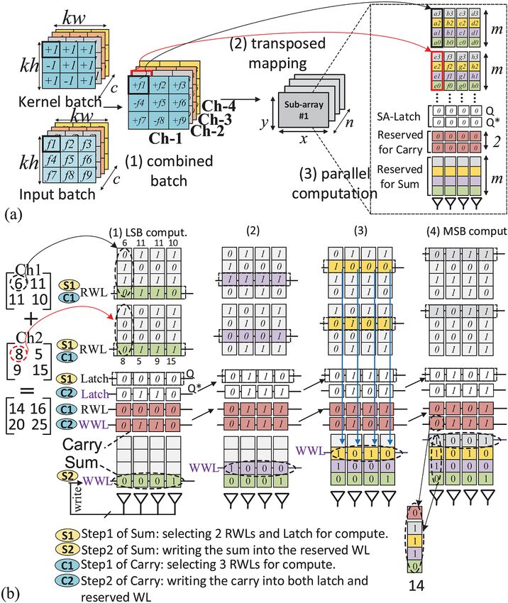
     c) Area Overhead: To estimate the area overhead of                            deep neural networks,” in Proceedings of the 45th Annual International
                                                                                   Symposium on Computer Architecture. IEEE Press, 2018, pp. 383–396.
two configurations of MRAM platform, three main hardware                       [8] S. Angizi, Z. He, and D. Fan, “Parapim: a parallel processing-in-memory
cost sources must be taken into consideration. First, add-                         accelerator for binary-weight deep neural networks,” in Proceedings of
on transistors to SAs connected to each BL. Second, the                            the 24th Asia and South Pacific Design Automation Conference. ACM,
                                                                                   2019, pp. 127–132.
modified MRD overhead; we modify each W L driver by                            [9] S. Angizi et al., “Dima: a depthwise cnn in-memory accelerator,” in
adding two more transistors in the typical buffer chain. Third,                    ICCAD. IEEE, 2018, pp. 1–8.
the Ctrl’s overhead to control enable bits; ctrl generates the                [10] S. Angizi, J. Sun, W. Zhang, and D. Fan, “Aligns: A processing-in-
                                                                                   memory accelerator for dna short read alignment leveraging sot-mram,”
activation bits with MUX units with 6 transistors. Overall,                        in Proceedings of the 56th Annual Design Automation Conference 2019.
the presented processing-in-MRAM platform based in SA-I                            ACM, 2019, p. 144.
imposes 5.8% overhead to main memory die, where SA-II                         [11] S. Angizi and D. Fan, “Graphide: A graph processing accelerator
                                                                                   leveraging in-dram-computing,” in GLSVLSI. ACM, 2019, pp. 45–50.
imposes 7.9%. Fig. 7 reports such area overhead breakdown                     [12] S. Angizi, Z. He, F. Parveen, and D. Fan, “Rimpa: A new reconfigurable
for two configurations.                                                            dual-mode in-memory processing architecture with spin hall effect-
                                                                                   driven domain wall motion device,” in ISVLSI. IEEE, 2017, pp. 45–50.
                                                                              [13] S. Angizi, Z. He, A. Awad, and D. Fan, “Mrima: An mram-based in-
                                                                                   memory accelerator,” IEEE Transactions on Computer-Aided Design of
                                                                                   Integrated Circuits and Systems, 2019.
                                                                              [14] X. Fong et al., “Spin-transfer torque devices for logic and memory:
                                                                                   Prospects and perspectives,” IEEE TCAD, vol. 35, 2016.
                                                                              [15] Z. He et al., “High performance and energy-efficient in-memory com-
                                                                                   puting architecture based on sot-mram,” in NANOARCH. IEEE, 2017,
                                                                                   pp. 97–102.
                                                                              [16] S. Angizi, Z. He, N. Bagherzadeh, and D. Fan, “Design and evaluation
                                                                                   of a spintronic in-memory processing platform for nonvolatile data
                    (a)                                 (b)                        encryption,” IEEE Transactions on Computer-Aided Design of Integrated
Fig. 7. Area overhead of processing-in-MRAM platform with (a) SA-I and             Circuits and Systems, vol. 37, no. 9, pp. 1788–1801, 2017.
(b) SA-II.                                                                    [17] S. Jain et al., “Computing in memory with spin-transfer torque magnetic
                          V. C ONCLUSION                                           ram,” IEEE TVLSI, pp. 470–483, 2018.
                                                                              [18] V. Seshadri et al., “Ambit: In-memory accelerator for bulk bitwise
   In this paper, we reviewed some of our recent Processing-                       operations using commodity dram technology,” in Micro. ACM, 2017,
in-Memory accelerators based on MRAM computational sub-                            pp. 273–287.
                                                                              [19] R. Andri, L. Cavigelli, D. Rossi, and L. Benini, “Yodann: An architecture
arrays to efficiently accelerate the inference process of                          for ultralow power binary-weight cnn acceleration,” IEEE Transactions
BWNNs within digital non-volatile memory rather than us-                           on Computer-Aided Design of Integrated Circuits and Systems, vol. 37,
ing analog crossbar operation. We especially investigated the                      no. 1, pp. 48–60, 2017.
                                                                              [20] S. Li et al., “Pinatubo: A processing-in-memory architecture for bulk
performance of two distinct in-memory addition schemes                             bitwise operations in emerging non-volatile memories,” in 2016 53nd
compared to other digital methods based on processing-in-                          DAC. IEEE, 2016.
DRAM/GPU/ASIC design to tackle DNN power and memory                           [21] S. Angizi, J. Sun, W. Zhang, and D. Fan, “Graphs: A graph processing
                                                                                   accelerator leveraging sot-mram,” in 2019 Design, Automation & Test in
wall bottleneck.                                                                   Europe Conference & Exhibition (DATE). IEEE, 2019, pp. 378–383.
                   ACKNOWLEDGEMENTS
                                                                              [22] S. Angizi and D. Fan, “Imc: energy-efficient in-memory convolver
  This work is supported in part by the National Science                           for accelerating binarized deep neural network,” in Proceedings of the
                                                                                   Neuromorphic Computing Symposium. ACM, 2017, p. 3.
Foundation under Grant No. 1740126, Semiconductor Re-                         [23] (2011)        Ncsu      eda      freepdk45.       [Online].    Available:
search Corporation nCORE, Cyber Florida Collaborative Seed                         http://www.eda.ncsu.edu/wiki/FreePDK45:Contents
Award Program and UCF NSTC Research Seed Award.                               [24] X. Dong et al., “Nvsim: A circuit-level performance, energy, and
                                                                                   area model for emerging non-volatile memory,” in Emerging Memory
                             R EFERENCES                                           Technologies. Springer, 2014, pp. 15–50.
 [1] S. Zhou, Y. Wu, Z. Ni, X. Zhou, H. Wen, and Y. Zou, “Dorefa-net:         [25] S. Li, D. Niu, K. T. Malladi, H. Zheng, B. Brennan, and Y. Xie, “Drisa:
     Training low bitwidth convolutional neural networks with low bitwidth         A dram-based reconfigurable in-situ accelerator,” in Proceedings of the
     gradients,” arXiv preprint arXiv:1606.06160, 2016.                            50th Annual IEEE/ACM International Symposium on Microarchitecture.
 [2] M. Courbariaux et al., “Binaryconnect: Training deep neural networks          ACM, 2017, pp. 288–301.
     with binary weights during propagations,” in Advances in Neural Infor-   [26] K. Chen, S. Li, N. Muralimanohar, J. H. Ahn, J. B. Brockman, and N. P.
     mation Processing Systems, 2015, pp. 3123–3131.                               Jouppi, “Cacti-3dd: Architecture-level modeling for 3d die-stacked dram
 [3] J. Song, “Binary generative adversarial networks for image retrieval,”        main memory,” in Proceedings of the Conference on Design, Automation
     arXiv preprint arXiv:1708.04150, 2017.                                        and Test in Europe. EDA Consortium, 2012, pp. 33–38.
 [4] P. Chi, S. Li, C. Xu, T. Zhang, J. Zhao, Y. Liu, Y. Wang, and            [27] S. D. C. P. V. . Synopsys, Inc.
     Y. Xie, “Prime: A novel processing-in-memory architecture for neural     [28] N. Muralimanohar et al., “Cacti 6.0: A tool to model large caches,” HP
     network computation in reram-based main memory,” in ACM SIGARCH               Laboratories, pp. 22–31, 2009.
     Computer Architecture News, vol. 44, no. 3. IEEE Press, 2016, pp. 27–
     39.
You can also read