E2v CMOS (and CCD) sensors (and systems) for astronomy - Paul Jorden BNL PACCD2016 1 Dec 2016
←
→
Page content transcription
If your browser does not render page correctly, please read the page content below
e2v CMOS (and CCD) sensors
           (and systems) for astronomy

                               Paul Jorden
                        BNL PACCD2016 1 Dec 2016

WE PARTNER WITH OUR CUSTOMERS TO IMPROVE, SAVE AND PROTECT PEOPLE’S LIVES
                                                                      1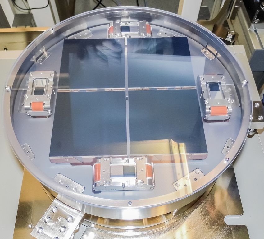
Contents-1
 E2v manufactures silicon sensors and systems for ground-based astronomy and space use

e2v designs and manufactures an increasing suite of CMOS imagers for high performance use

                              1.    CMOS Sensors achieve maturity
                    •   Custom Backthinned CMOS sensors for ground-based astronomy
                                 • Custom CMOS sensors for space use
                                       • Standard CMOS sensors
                                        • CMOS developments

                                               2.   EM CCDs
                                           • Standard L3Vision sensors
                               •        Custom sensors for astronomy & science

                                   3.   Precision System assemblies
                                        •   The WUVS space sensor system
                                             • KMTNet focal planes
                                        •   The J-PAS OAJ Cryocam system

                                               4.   Summary
                                                                                            2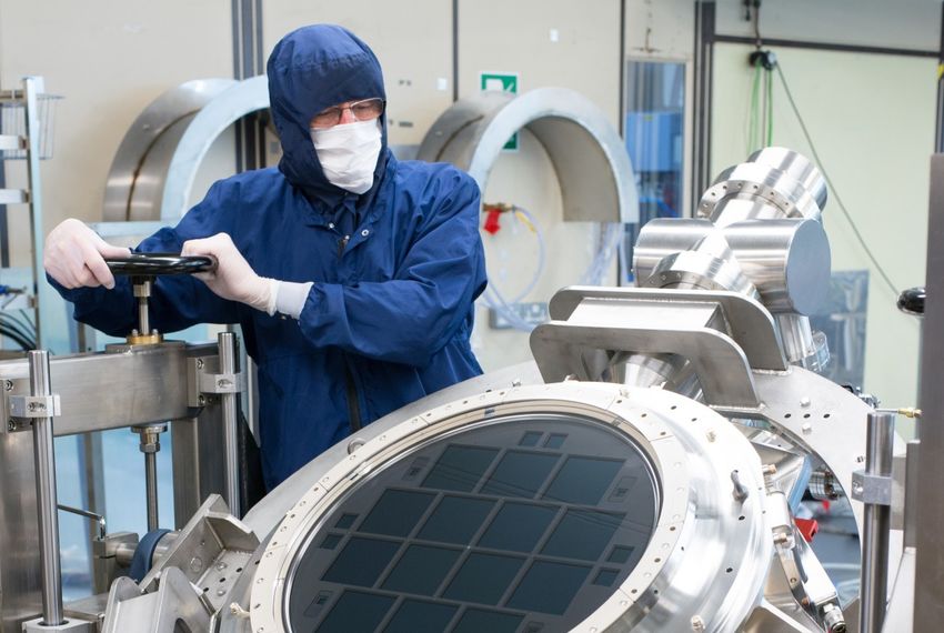
CMOS detectors-1
     CIS113                                   Number of pixels     1920 (H) × 4608 (V)
   Developed for the TAOS-II project.         Pixel size           16.0 µm square
   Development complete; production           Image area           73.73m × 30.72 mm
   in progress; 10 delivered; full set of
   40 due for completion by Jan 2017          Output ports         8 (REF and SIG each)
                                              Package size         82.39 mm × 31.7 mm
                                                                   76 pin ceramic PGA
                                              Package format
                                                                   attached to invar block
                                              Focal plane height   14.0 mm
                                              Flatness             < 30 µm (peak - valley)
                                              Conversion gain      75 µV/e−
                                              Readout noise        3 e− at 2 MP/s per ch.
                                              Maximum pixel rate   2 MP/s per channel
                                              Maximum charge       22,000 e− per pixel
                                              Dark signal          70 e−/pixel/s (at 21 °C)
                                                                   2 fps (full frame mode)
Paper by Jérôme Pratlong, 9915, Tues am, S8   Frame rate
                                                                   20 fps (multiple ROI’s)
                                                                                              3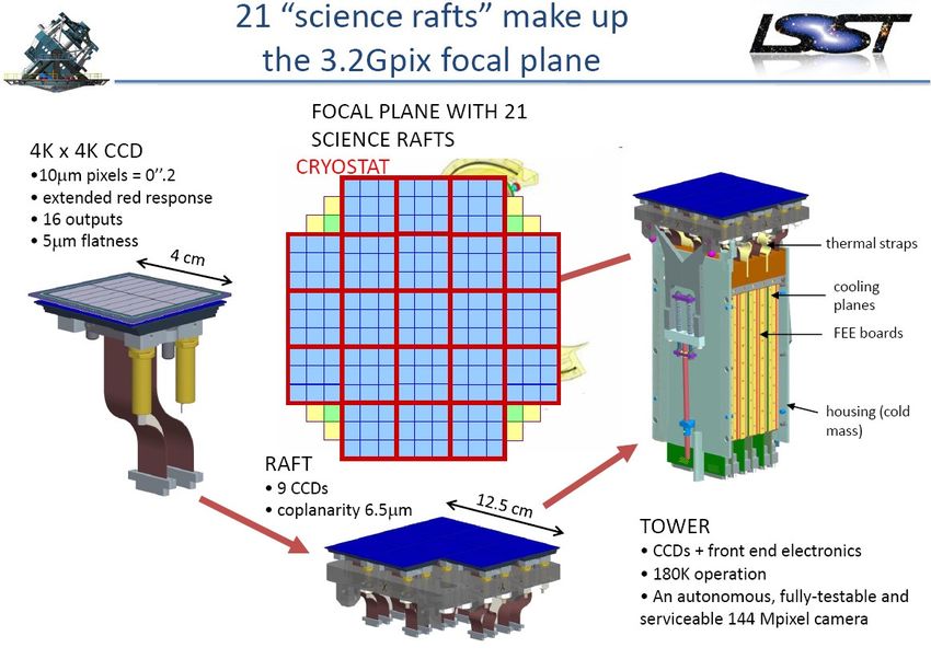
CMOS detectors-3
         Onyx EV76C664

                                                                    Key Features
•   Standard product with low noise
•   Fully digital sensor with multiple modes                          1280 X 1024
                                               Number of pixels
                                                                      (1.3 Megapixel)
•   Frontside illuminated with micro-lens
                                               Pixel size             10.0 µm square

                                               Shutter modes          Global and Rolling

                                               Output                 8, 10, 12, 14 bit LVDS

                                               Package format         Ceramic 67-pin PGA

                                               Readout noise          6 e− (min, depending on mode)
                                                                      Monochrome or sparse colour
                                               Quantum Efficiency
                                                                      (with microlens)
                                               Maximum charge         16,000 e−    per pixel

                                                            See e2v.com for datasheet

                                                                                                      5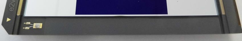
CMOS detectors-4
          CIS115
                                                Number of pixels                1504(H) × 2000(V)
•   Backthinned sensor with low read-noise      Pixel size                      7.0 µm square
•   Designed for space applications             Number of output ports          4 pairs of analogue
•   Planned for JANUS (Juice) ESA mission       (reset and signal pins)         outputs
•   Being qualified for space use by end-2016   Package size                    48.26 mm square
•   Samples available; FMs to follow            Package format                  140 pin ceramic PGA

                                                Flatness                        < 10 µm (peak to valley)

                                                Conversion gain                 35 µV/e−

                                                Readout noise                   7 e− (Rolling shutter)

                                                Maximum pixel data rate         8 MP/s per channel

                                                Maximum charge per pixel        55,000 e−

                                                Frame rate                      Up to 10 Hz
                                                Minimum time to read one
                                                                                66.25 µs
                                                line at 6·2 MP/s
                                                Frame rate at full resolution   Up to 7.5 fps

                                                                                                         6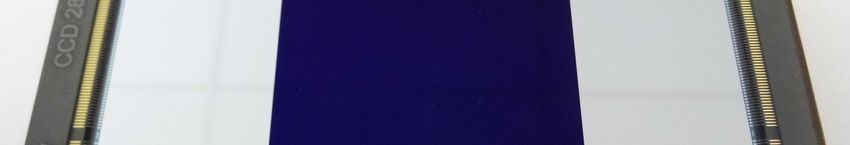
CMOS detectors-5
   TDI CMOS development

Time-Delay-Integrate used for scanning space applications; eg GAIA uses TDI CCDs
•  TDI CMOS offers digital architecture & low power
•  Most promising technique is a CCD-like structure-
•  Charge summation along track
•  Good CTE after irradiation is important
•  Small test devices made & tested
•  Full sized device planned

See paper by F Mayer, IISW 2015 on e2v.com
                                                                                   7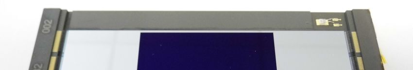
CMOS detectors-6
CIS111 (MTG FCI)

 •   Example of imager used for earth observation-
 •   Offers higher frame rate and lower crosstalk than an equivalent CCD
 •   CIS111 to be used on Meteosat Third Generation Flexible Combined Imager
 •   5 independent imager blocks with in-package filters
 •   Rhombus shaped pixels in outer blocks
 •   Optimised for good transfer through large pixels and low lag

                                CIS111 architecture
                                                                               8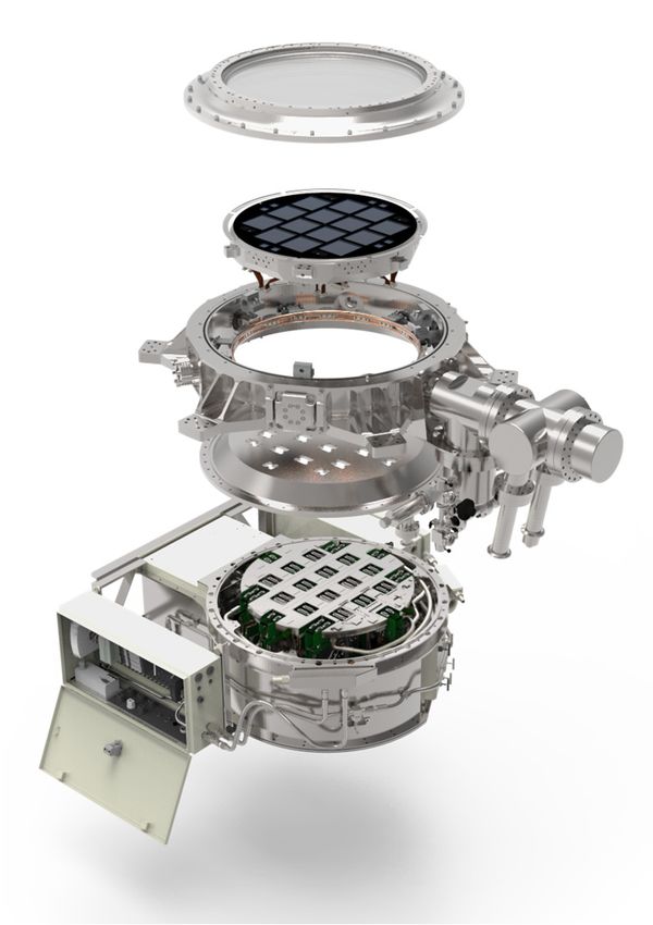
CMOS detectors-7
CIS116 (Metimage)

       Custom test vehicle with 250 um square pixels
       •  Each pixel has 8 photodiodes with a common sense node
       •  Aims to optimise lag and Charge-Voltage-Factor
       •  2.5 Me- peak signal; 84 dB dynamic range
       •  Designed for backthinning
       •  Test devices have been characterised

                                                        CIS116 pixels

                                                                        9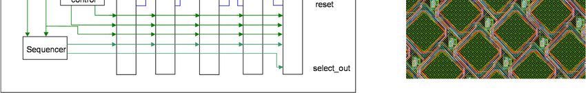
CMOS detectors-8
  CIS120
                                                 Number of pixels:             2048(H) × 2048(V)
Easy to use general purpose imager for space
                                                 Pixel size:                   10.0 µm square
                                                                               Ceramic-PGA or
                                                 Package format:
                                                                               3-side buttable option
                                                 Maximum charge per pixel:     50,000 e−

                                                 Readout noise:                4 e− (Rolling shutter)

                                                 Conversion gain:              45 µV/e−

                                                 Back-thinned QE:              90% at 550 nm

                                                 Frame rate:                   30 fps @ 8 bit resolution

                                                 Power consumption:            350 mV (full LVDS)

                                                 4 LVDS outputs                8, 10, 12, 14 bits ADC

                                               Rolling and global shutter; SPI programmable configuration
                                               Digital outputs. Designed to be radiation tolerant

                                                   Front-illuminated samples due for test- Mar 2017
Layout plot           Package example              Back-illuminated samples due for test- 4Q 2017

                                                                                                        10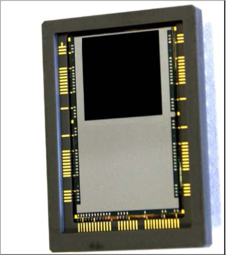
CMOS detectors-9 …

Fully Depleted, Monolithic PPD CMOS Image
Sensor Using Reverse Substrate Bias

Konstantin Stefanov
Centre for Electronic Imaging (CEI)
Background

• Demand for thick (>100 µm), fully depleted CMOS sensors for high QE
• Near-IR imaging for astronomy, Earth observation, hyperspectral
  imaging, high speed imaging, spectroscopy, microscopy and surveillance.
• Soft X-ray (200 µm
• Low voltage CMOS sensors normally have small depletion depths

                e2v CIS115

                                   12                  Konstantin Stefanov, 17 November
                                                       2016
Reverse biasing PPD pixels
P-wells • If reverse bias Vreverse is applied:
– p+/p/p+ resistor is formed, leakage
+Bias +Bias +Bias
current flows
– This has to be eliminated for a
Diode practical device
• Pinch-off under the p-wells is needed at
all times (merged depletion regions) to
prevent leakage
Pinch-off
• The pinch-off condition depends on:
P-type – Doping and junction depth
epi/bulk – Photodiode and p-well sizes
Si – Bias voltages
Backside p+ implant
–Vreverse – Stored signal charge
• P-wells should be narrow and shallow
• Photodiodes should be deep
13 Konstantin Stefanov, 17 November
2016Substrate current suppression
• If the p-wells are deep (as they are
usually), pinch-off may not occur
Simplified PPD pixel
• The p-well should be made to be as
structure narrow as possible, but this is not
Diode p-well Diode p-well Diode sufficient
• The CMOS structure makes pinch-off
harder to achieve than “high rho” CCDs
• Additional n-type implant added:
– Under the p-wells
– Floating
Additional implants – Not connected to anything
– Called Deep Depletion Extension
(DDE)
• Patent pending (owned by e2v
Technologies)
• Can be applied to any existing design
14 Konstantin Stefanov, 17 November
2016Potentials
Guard p-well Diode p-well Diode p-well Diode
ring
DDE Implant No implant
The DDE implant extends the diode
depletion sideways under the p-wells
15 Konstantin Stefanov, 17 November
2016The first chip (BSB1)
• Made on 18 µm 1 kΩ.cm epi, as a proof of principle
– This reverse bias method applies to any thickness
• Prototyping 10 µm and 5.4 µm pixel designs
– 8 pixel arrays of 32 (V) × 20 (H) pixels each
• Each array explores different shape and size of the
DDE implant
– One reference design without DDE (plain PPD
pixel)
• Custom ESD protection designed
• Delivered in July 2016
• Characterisation goals:
– Reverse bias and current, prove full depletion
– Gain, linearity, image lag; comparison with non-
modified PPD pixel
– Over-illumination
– X-ray response
18 Konstantin Stefanov, 17 November
2016Reverse biasing
Measurement Simulation for high Vpin
• This shows the reverse current for the whole chip, including the logic and ESD pads
• All pixel variants work
• Reverse bias above -5V with no leakage means that any thickness can be depleted
– VBSB = -4V fully depletes 18 µm thick epi, 1 kΩ.cm
• Qualitative agreement with the simulations
– The measurement is for all 8 variants in parallel, simulation is for one variant only
20 Konstantin Stefanov, 17 November
2016Electro-optical performance
• Photon transfer curves taken under various
conditions
• 10 µm pixel:
– CVF ≈ 80 µV/e- (design = 70 µV/e-)
– FWC ≈ 15 ke- (design = 20 ke-, limited by
the sense node)
– Noise (in our system) ≈ 8 e- RMS
• 5.4 µm pixel:
– CVF ≈ 36 µV/e- (design = 33 µV/e-)
10 µm pixel – FWC ≈ 15 ke- (design = 45 ke-, limited by
the sense node and off-pixel circuits)
• The new pixels appear identical to the
“normal” pixels
• The DDE implant and the reverse bias do not
seem to affect the electro-optical
performance – great!
22 Konstantin Stefanov, 17 November
2016Conclusions
• New development of fully depleted monolithic PPD CMOS sensors using
reverse substrate bias
– A paper in IEEE Electron Device Letters (in press)
• Based on the idea of “depletion extension”
• First prototype designed on 18 µm, 1 kΩ.cm epi as a proof of principle
– Can be scaled to much thicker epi/bulk substrates
– Front-face results shown here
– Back-thin (demo device) to be tested ~ March 2017
– Aim to design & make 40 um thick imager next……
• Can be attractive to large number of applications
– High QE on a par with thick CCDs and hybrid CMOS
– Low noise, 4T architecture with minimum changes
• Competitor to scientific CCDs?
23 Konstantin Stefanov, 17 November
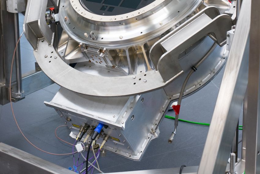
2016CCDs with high red sensitivity
LSST CCD250
4k X 4k 10 µm format
189 science sensors
100 µm thick; 5 um flat
High precision SiC
buttable package
16 outputs; 2 s readout
5 e- read-noise
Pictures courtesy: LSST
24Contents-2
We illustrate selected EMCCDs
Internal electron gain allows sub-electron read-noise
Combined with backthinned spectral response for very high sensitivity
Several formats and sizes available
Standard (non EMCCDs) are not discussed in this presentation- many are visible on e2v.com
2. EM CCDs
• Standard L3Vision sensors
• Custom sensors for astronomy & science
25CCD sensors-1
CCD201
• Standard product See e2v.com
• 1024 X 1024 pixels; 13 µm pixels for datasheet
• Larger format than CCD97 (512 X 512 pixels)
• Widely used for commercial applications
• Also useful for astronomy at low signal levels
• Sub-electron read noise
• Backthinned for high spectral response
• Inverted mode dark current
Planned for Space use : NASA WFIRST Coronagraph
Harding L, et al, “Technology advancement of the CCD201-20 EMCCD for the
WFIRST-AFTA Coronagraph Instrument…,” JATIS 011007, (2016).
See poster by Nathan Bush, 9904, Tues pm
26CCD sensors-2
CCD282
• Largest EMCCD manufactured to date
• 4096 X 4096 pixel image area
• Split frame-transfer read-out with 8 outputs
• > 4 frames per second
• Sub-electron read-noise
• Backthinned for high Quantum Efficiency
• Very low levels of clock-induced charge
• Non-inverted operation at cryogenic
temperatures
• Development is complete; sensors have
been delivered
Gach Jean-Luc, et al, “Development of a 4kx4k frame transfer electron multiplying CCD
for scientific applications,” Proc SPIE 9154, (2014).
27CCD sensors-3
CCD351
• Standard product, for commercial use Typical Performance
• L3Vision technology for sub-electron
read-noise Image section 1024 x 1024
• Video rate readout Pixel size 10 µm × 10 µm
• Backthinned spectral response
Active image area 10.24 × 10.24 mm
• In standard production
Package size 22.86 × 28.00 mm
Amplifier
3.5 µV/e−
responsivity
Readout noise < 1 e- (with EM gain)
Multiplication gain 100-1000 typical
Output data rate 37 MHz
Pixel charge storage 35 ke-/pixel
Dark signal (18°C) 100 e-/pixel/s
Package illustration (not final)
28Contents-3
e2v develops sub-systems to complement its supply of sensors.
• Bespoke systems are optimised for each application and use common modules where
appropriate.
• Performance of sensors combined with system can be guaranteed.
3. Precision System assemblies
• The WUVS space sensor system
• KMTNet focal planes
• The J-PAS OAJ Cryocam system
29Precision System Assemblies-1
WUVS
World Space Observatory UV Spectrograph
• 115-310 nm range covered by three sensor channels
• Custom sealed vacuum cryostat enclosures for 9 year life
• with flight electronics (associated with RAL Space)
• UV optimised custom CCD272 operated at -100°C
• Components maintain alignment after shock & vibration of launch
• Design and manufacture underway
30Precision System Assemblies-2
WUVS
Triple detector unit detector layout with camera electronics units
See Poster by Vladimir Panchuk, 9905, Sun pm
31Precision System Assemblies-3
KMTNet focal planes
Korea Micro-lensing Telescope Network
3 telescopes each with its own camera; 350 mm focal plane; 340 MegaPixel each
Each camera had four CCD290 science sensors and four guide sensors; < 30 µm flatness
Focal planes are complete (e2v) , operational and installed in cameras (by Ohio State University)
See Poster by Dae-Sik Moon, 9906, Mon pm. Also see previous paper Jorden et al, SPIE 2014
32Precision System Assemblies-4
J-PAS Cryocam
A 1.2 Gigapixel cryocam for use on the 2.5m OAJ telescope for the J-PAS survey.
e2v has delivered (mid-2016) this important commercially-suppled astronomical camera
33Precision System Assemblies-5
J-PAS Cryocam
Table of key features
450 mm focal plane diameter -100ºC operating temperature Stable to +/- 0.5ºC
27 µm peak-valley flatness Measured at -100C Stable against flexure
14 science CCD290-99 sensors: 1.2 Gig pixels 9K X 9K sensors
8 wavefront sensors: CCD44-82 FT Custom packages
4 guide sensors: CCD47-20 FT Custom packages
Integrated electronics 224 science channels < 5 e- read-noise at 400 kHz
Modular CCD drive units Synchronized readout of Local frame stores
science CCDs
Complete LN2 cooling system Integrated vacuum system Post-delivery support
Cold light baffle High Quantum Efficiency minimum reflection AR coat
See paper by Mark Robbins, 9908, Tues 28 June 2016, am, S8
And K Taylor et al, JPCAM, JAI vol 3, 2014
34Summary
• An increasing number of sensors are being developed using CMOS
architectures
Many of these are backthinned and offer low read-noise (comparable to CCDs)
• CCDs continue to be used in larger quantities and with greater heritage
• e2v offers custom system solutions including cryogenic cameras and
electronic modules to complement its supply of sensors- and with
guaranteed performance
Thank you for your attention
35WE PARTNER WITH OUR CUSTOMERS TO IMPROVE,
SAVE AND PROTECT PEOPLE’S LIVES
OUR INNOVATIONS LEAD DEVELOPMENTS IN COMMUNICATIONS, AUTOMATION,
DISCOVERY, HEALTHCARE AND THE ENVIRONMENT 36You can also read