EDSADC_1 for KIT_AURIX_TC375_LK - Enhanced Delta-Sigma ADC conversion AURIX TC3xx Microcontroller Training - Infineon Technologies
←
→
Page content transcription
If your browser does not render page correctly, please read the page content below
EDSADC_1
for KIT_AURIX_TC375_LK
Enhanced Delta-Sigma ADC conversion

AURIX™ TC3xx Microcontroller Training
V1.0.0
 Please read the Important Notice and Warnings at the end of this document
Scope of work

The EDSADC is used to convert an external signal to a stream of
discrete digital values.

The Enhanced Delta-Sigma ADC (EDSADC) continuously measures an
external signal on channel 3, connected to port pin AN0. It converts the
analog signal to a data stream and then a global variable is updated to the
current conversion result. The input value is determined by the potentiometer
on the board.

 Copyright © Infineon Technologies AG 2021. All rights reserved.
Introduction

› The Enhanced Delta-Sigma Analog-to-Digital Converter module
 (EDSADC) of the AURIX™ TC37x provides a set of up to 6 analog input
 channels

› Each converter channel is controlled by a dedicated set of registers, which
 enables the independent operation of the channels

› The results of each channel can be stored in a channel-specific result
 register. They are signed values stored in a 16-bit two’s complement
 format

› To compensate manufacturing tolerances and adjust the channel to the
 selected decimation rate, a calibration algorithm is executed automatically
 by hardware

› The calibration algorithm can be enabled both during the initialization
 phase and during operation

 Copyright © Infineon Technologies AG 2021. All rights reserved.
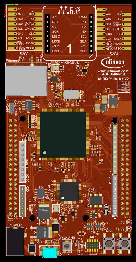
Hardware setup

This code example has been developed for the
board KIT_A2G_TC375_LITE.

In this example, the pin AN0, connected to the
board’s potentiometer, is used.

 Copyright © Infineon Technologies AG 2021. All rights reserved.
Implementation

Configuration of the EDSADC module:

Configuration of the EDSADC module is done once in the setup phase by calling the initialization
function init_EDSADC(), which contains the following steps:

› EDSADC module configuration
› EDSADC channel configuration

EDSADC module configuration

To configure the EDSADC module, the following steps are done:

1. The module configuration is filled with default values using an instance of the structure
 IfxEdsadc_Edsadc_Config and the function IfxEdsadc_Edsadc_initModuleConfig()
2. The modulator clock is set to be generated independently of the Phase Synchronizer signal
3. The EDSADC module is then initialized with the function IfxEdsadc_Edsadc_initModule()

 Copyright © Infineon Technologies AG 2021. All rights reserved.
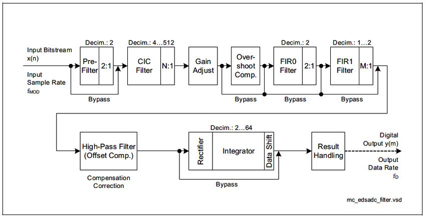
Implementation

EDSADC channel configuration

To configure the EDSADC channel, the following steps are done:

1. The channel configuration is created with an instance of the structure
 IfxEdsadc_Edsadc_ChannelConfig and filled with default values using the function
 IfxEdsadc_Edsadc_initChannelConfig()
2. The comb filter decimation factor and start value are set
3. The FIR filters in the filter chain are enabled (as shown in Slide 7) and the trigger for starting the
 calibration during the initialization phase is set
4. The modulator is configured by setting its frequency and internally connecting the negative input
 to the ground, in order to configure the conversion in single-ended mode
5. The channel ID is selected and the calculated Cascated Integrator Comb (CIC) filter‘s shift and
 gain factor are set
6. The intended full-scale value is set (by default, it is set to 25000 after reset)
7. Finally, the channel is initialized with the function IfxEdsadc_Edsadc_initChannel() and the
 conversion is started using the function IfxEdsadc_Edsadc_startScan()

All the previous functions are provided by the iLLD header IfxEdsadc_Edsadc.h.

 Copyright © Infineon Technologies AG 2021. All rights reserved.
Implementation

Configured filter chain

 Copyright © Infineon Technologies AG 2021. All rights reserved.
Implementation

Factors calculation

› To achieve a correct calibration, the values for the CIC shift and gain factor must be calculated
 according to the intended full-scale value and the selected decimation factor

› The value for the CIC shift is determined by the formula:

 = roundup(14 − log 2 (2 ∗ / ( 3 ∗ 4 ∗ ))

 where
 – N is the selected decimation factor
 – AFS is the intended calibrated full-scale value (it refers to the analog full-scale = )
 – FM is the modulator gain factor (when using the on-chip modulator FM = 0,6945)

› The gap that comes from the rounding in the above formula is closed by computing the
 corresponding gain correction factor:

 gain factor = (2 ∗ / 3 ∗ 4 ∗ ) ∗ 2(−14)

 That is then multiplied by 4096 and truncated to be stored in the GAINFACTOR bitfield of
 GAINCORR register

 = truncate( gain factor * 4096 )

 Copyright © Infineon Technologies AG 2021. All rights reserved.
Implementation

Example calculation

› For example, using the on-chip modulator (thus FM = 0,6945), selecting a decimation factor N = 32 and an
 intended full-scale value AFS = 30000

› The value for the CIC shift is determined by the formula:

 = roundup(14 − log 2 (2 ∗ / ( 3 ∗ 4 ∗ ))
 = roundup(14 − log 2 (2 ∗ 30000/(323 ∗ 4 ∗ 0,6945))
 = roundup(14 − log 2 (0,6591))
 = roundup(14 − (−0,6013)) = roundup(14,6013) = 15
› And the gain correction factor

 gain factor = (2 ∗ / 3 ∗ 4 ∗ ) ∗ 2(−14)
 = 0,6591 ∗ 215−14 = 0,6591 ∗ 2 = 1,3182

 Which gives a GAINFACTOR bitfield of

 = truncate( gain factor * 4096 )
 = truncate( 1,3182 * 4096 )
 = truncate( 5399,3472 ) = 5399

 Copyright © Infineon Technologies AG 2021. All rights reserved.
Implementation

The conversion function:

› The run_EDSADC() function is called in the while loop and continuously converts the analog
 voltage level on channel 3 to a digital value

› The function IfxEdsadc_Edsadc_getMainResult() from the iLLD header IfxEdsadc_Edsadc.h is
 used to get the latest analog to digital conversion. The digital result of EDSADC is stored in two’s
 complement format

› Finally, the voltage value is calculated scaling the EDSADC raw value to the range 0 – 3.3V,
 considering the intended full-scale value set in the configuration

 Copyright © Infineon Technologies AG 2021. All rights reserved.
Run and Test

After code compilation and flashing the device, perform the following steps:

› The signal to be measured (0 V to +3,3 V) is controlled via the potentiometer
› In order to get the global variable in a stable state, the debugger should be paused
 or a breakpoint should be inserted in the function run_EDSADC()
› The measured value can be watched through the debugger in the
 g_resultEDSADC variable and the converted value in the g_resultVoltage
 variable

 Copyright © Infineon Technologies AG 2021. All rights reserved.
References

 › AURIX™ Development Studio is available online:
 › https://www.infineon.com/aurixdevelopmentstudio
 › Use the „Import...“ function to get access to more code examples.

 › More code examples can be found on the GIT repository:
 › https://github.com/Infineon/AURIX_code_examples

 › For additional trainings, visit our webpage:
 › https://www.infineon.com/aurix-expert-training

 › For questions and support, use the AURIX™ Forum:
 › https://www.infineonforums.com/forums/13-Aurix-Forum

 Copyright © Infineon Technologies AG 2021. All rights reserved.
Trademarks
All referenced product or service names and trademarks are the property of their respective owners.

Edition 2021-03 IMPORTANT NOTICE For further information on the product,
Published by The information given in this document shall in no technology, delivery terms and conditions and
Infineon Technologies AG event be regarded as a guarantee of conditions or prices please contact your nearest Infineon
81726 Munich, Germany characteristics (“Beschaffenheitsgarantie”) . Technologies office (www.infineon.com).
 With respect to any examples, hints or any typical
© 2021 Infineon Technologies AG. WARNINGS
 values stated herein and/or any information
All Rights Reserved. Due to technical requirements products may
 regarding the application of the product, Infineon
 contain dangerous substances. For information
 Technologies hereby disclaims any and all
Do you have a question about this on the types in question please contact your
 warranties and liabilities of any kind, including
document? nearest Infineon Technologies office.
 without limitation warranties of non-infringement
Email: erratum@infineon.com
 of intellectual property rights of any third party. Except as otherwise explicitly approved by
 Infineon Technologies in a written document
Document reference In addition, any information given in this
 signed by authorized representatives of Infineon
EDSADC_1_KIT_TC375_LK document is subject to customer’s compliance
 Technologies, Infineon Technologies’ products
 with its obligations stated in this document and
 may not be used in any applications where a
 any applicable legal requirements, norms and
 failure of the product or any consequences of the
 standards concerning customer’s products and
 use thereof can reasonably be expected to result
 any use of the product of Infineon Technologies in
 in personal injury.
 customer’s applications.
 The data contained in this document is exclusively
 intended for technically trained staff. It is the
 responsibility of customer’s technical
 departments to evaluate the suitability of the
 product for the intended application and the
 completeness of the product information given in
 this document with respect to such application.
You can also read